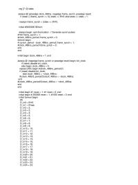
Archives
Chapter 10 Note that Ready is effectively a Moore signal
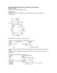
Prentice Hall, Pearson Education, 2011 Problem 10-2 The STG of Figure 10-19(b) has been modified to handle an empty multiplier or multiplicand. Note that Ready is effectively a Moore signal. module Prob_10_2_Multiplier_STG_0 #(parameter L_word = 4)( output [2*L_word -1: 0] […]
Chapter 10 Start Clock Reset Exhaustive Testbench Reg 2 word size
endmodule module test_Multiplier_RR_ASM (); parameter word_size = 4; wire [2*word_size: 0] product; //wire Done; initial #80000 $finish; // Timeout always @ (posedge clock) // Compare product with expected value if (Start) begin #5 expected_value <= 0; expected_value <= word2 * […]
Chapter 10 This Done Each Clock Until Num shift divisor Reduced
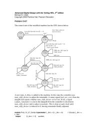
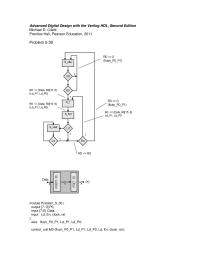
Copyright 2009 Prentice Hall, Pearson Education Problem 10-27 The control unit of the modified machine has the STG shown below: A new state, A_Rem, is added to the machine. In this state the controller uses num_shift_divisor to adjust the remainder. […]
Chapter 11 As the cells of the counter pass through transient
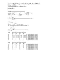
Prentice Hall, Pearson Education, 2011 Problem 11-1 In_0 In_1 In_2 In_3 In_4 Out_1 G1 (4:5, 6:7) (2:3, 3:4) (3:4, 5:6) (3:4, 5:6) In_0 In_1 In_2 In_3 In_4 Out_1 Out_0 P1 P2 P3 P4 P5 P6 (4:5, 6:7) Out_0 G0 G2G3 […]
Chapter 2 Boolean expression in SOP form is canonical
Advanced Digital Design with the Verilog HDL, Second Edition Michael D. Ciletti Prentice Hall, Pearson Education, 2011 Problem 2-1 Recall that a minterm is a cube in which every variable appears. A Boolean expression in SOP form is canonical if […]
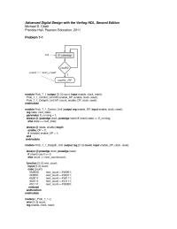
Chapter 3 Advanced Digital Design with the Verilog HDL
Problem 3-1 Advanced Digital Design with the Verilog HDL, Second Edition Michael D. Ciletti Prentice Hall, Pearson Education, 2011 Problem 3-2 Par_Detect ParityBit_in clk rst Assumption: asynchronous reset Bit_in clocked on rising edge. Interpretation: Even parity will be asserted unless […]
Chapter 4 The connectivity of the 16-bit adder will be
Prentice Hall, Pearson Education, 2011 Problem 4-1 module Combo_str (output Y, input A, B, C, D); and (Y, w1, w3); not (w1, w2); or (w2, A, D); and (w3, B, C, w4); not (w4, D); endmodule module t_Combo_str (); reg […]
Chapter 4 Use Nested For Loops Exhaustively Generate Input
Problem 4-11 c. Use nested for loops to exhaustively generate input patterns to the adder. for (c_in = 0; c_in <= 1; c_in = c_in + 1) … for(a = 0; a <= 15; a = a + 1) … […]
Chapter 5 Advanced Digital Design With The Verilog
Prentice Hall, Pearson Education, 2011 Problem 5-1 module Combo_CA (output Y, input A, B, C, D); assign Y = (~(A | D)) & (B & C & ~D); endmodule module t_Combo_CA(); reg A, B, C, D; wire Y; Combo_CA M0 […]
Chapter 5 Otherwise each receives the output of the mux connected
Prentice Hall, Pearson Education, 2011 Problem 5-30 module Problem_5_30 ( output [7: 0] P0, input [7:0] Data, input Ld, En, clock, rst ); wire flush_P0_P1, Ld_P1, Ld_P0; control_unit M0 (flush_P0_P1, Ld_P1, Ld_P0, Ld, En, clock, rst); Advanced Digital Design with […]
Chapter 5 Prentice Hall module Universal Shift
Problem 5-13 module Universal_Shift_Reg ( output reg [3:0] Data_Out, output MSB_Out, LSB_Out, input [3:0] Data_In, input MSB_In, LSB_In, input s1, s0, clk, rst); assign MSB_Out = Data_Out[3]; assign LSB_Out = Data_Out[0]; always @ (posedge clk) begin if first) Data_Out <= […]
Chapter 5 Verify operations for data read from registers
Prentice Hall, Pearson Education, 2011 Problem 5-25 module Prob_5_25 (output reg [7:0] count, input clk, rst_b); parameter s0 = 0, s1 = 1, s2 = 2, s3 = 3, s4 = 4, s5 = 5, s6 = 6, s7 = […]
Chapter 6 Initial bit sequence of first byte after first synch
reg [7: 0] state; always @ (posedge clock_488ns, negedge frame_synch, posedge reset) if (reset || (frame_synch == 0)) state <= 8’h0; else state <= state + 1; //assign frame_synch = (state == 8’hff); initial begin clock_488ns = 1; end always […]
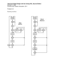
Chapter 6 Solution for resetting machine is not required
Prentice Hall, Pearson Education, 2011 Problem 6-4 Resetting machines: Advanced Digital Design with the Verilog HDL, Second Edition Michael D. Ciletti Prentice Hall, Pearson Education, 2011 Problem 6-5 Advanced Digital Design with the Verilog HDL, Second Edition Michael D. Ciletti […]
Chapter 7 Because the signals controlling the data path operations
Prentice Hall, Pearson Education, 2011 Problem 7-1 module Prob_7_1 (output [3: 0] count, input enable, clock, reset); Prob_7_1_Control_Unit M0 (enable_DP, enable, clock, reset); Prob_7_1_Datapth_Unit M1 (count, enable_DP, clock, reset); endmodule module Prob_7_1_Control_Unit (output reg enable_DP, input enable, clock, reset); reg […]
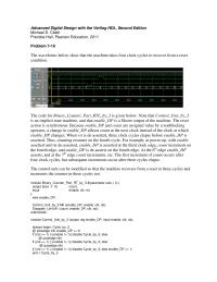
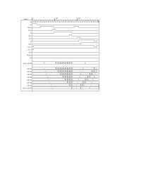
Chapter 7 The First Increment Count Occurs After Four
Prentice Hall, Pearson Education, 2011 Problem 7-10 The waveforms below show that the machine takes four clock cycles to recover from a reset condition. The code for Binary_Counter_Part_RTL_by_3 is given below. Note that Control_Unit_by_3 is an implicit state machine, and […]
Chapter 8 Note use of conditioned events for the address setup
Copyright 2009 Prentice Hall, Pearson Education Problem 8-6 module RAM_static (output data_out, input data_in, CS_b, WE_b); // Note: chip select and write are active-low always ( CD_b, WE_b, data_in) if (CS_b == 1’b0) &&(WE_b == 1’b0) data_out = data_in; else […]
Chapter 8 Parameters for the write cycle Verified in simulation
specparam t_ACS = 8; // Chip select access time specparam t_CLZ = 2; // Chip select to output in low-z // Parameters for the write cycle specparam t_WC = 7; // Write cycle time specparam t_CW = 5; // Chip […]
Chapter 9 Both responses display the filter’s tap coefficients
word_size = 16, word_size_out = 2*word_size + 2, write_ptr_size = 4, b0 = 8’d7, // Filter coefficients ); reg [word_size -1: 0] Sample_Array [0: FIR_order -1]; reg [write_ptr_size -1: 0] write_ptr; parameter max_write_ptr = 4’d7; integer k; always @ (posedge […]

Chapter 9 For Example The Array Could Partitioned Into
8 15 22 16 23 24 3 10 17 4 11 18 5 12 19 6 13 20 7 14 21 21 9 P1 P2 P3 t8t9t10 t11 t12 t13 t15 t16 t17 t18 t3t4t5t6t7t14 t1t2 Time slots 8 15 […]
Chapter 9 Instead Single Threshold There Distribution Thresholds
Name clk rst Ready Load ld done Sort gt 0100 200 t Busy j_gte_i i_lte_N Send Waiting snd Data_in[3:0] A1[3:0] A2[3:0] A3[3:0] A4[3:0] A5[3:0] A6[3:0] A7[3:0] Data_out[3:0] 0 x x 1 1 x 2 2 1 x 2 3 3 […]
Chapter 9 Replace for loop stop condition with numeric value
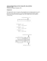
Prentice Hall, Pearson Education, 2011 Problem 9-2 The figures below show (1) registers of the datapath unit of an implementation of a pixel processor using a single processor, (2) a block diagram showing the interface signals between the control unit […]
Chapter 9 The block diagram of the concurrent processor
6)(); wire [1: H_bin_size*N_bins] Histogram_bits; wire Ready, Valid, Wait__P1, Wait_P2, Wait_P3, Wait_P4, Wait_P5, Wait_P6; reg [1: pixel_size * N_col * M_row] pixel_bits; reg Go, clk, reset; wire [H_bin_size: 0] Level1 = Histogram_bits [1: H_bin_size]; wire [H_bin_size: 0] Level2 = Histogram_bits […]
Chapter 9 where the FU receives the result of the previous
PV[39] = pixel_bits [38*pixel_size + 1: 39*pixel_size]; PV[40] = pixel_bits [39*pixel_size + 1: 40*pixel_size]; genvar m; generate for (m = 1; m <= N_col*M_row; m = m + 1) begin: FU if (m ==1) begin HPFU M (Histogram_memory[1], {H_bin_size*N_bins{1’b0}}, PV[1]); […]