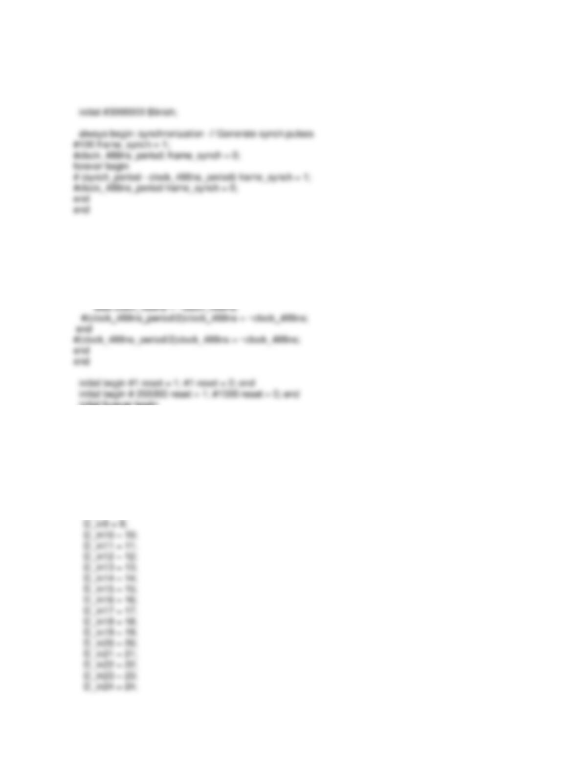
reg [7: 0] state;
always @ (posedge clock_488ns, negedge frame_synch, posedge reset)
if (reset || (frame_synch == 0)) state <= 8’h0; else state <= state + 1;
//assign frame_synch = (state == 8’hff);
initial begin clock_488ns = 1; end
always @ (negedge frame_synch or posedge reset) begin: bit_clock
if (reset) disable bit_clock;
else begin clock_488ns = 0;
repeat (255) begin #(clock_488ns_period/2)
if (reset) disable bit_clock;
initial forever begin
#5
D_in0 = 8’hff;
D_in1 = 8’haa;
D_in2 = 2;
D_in3 = 3;
D_in4 = 4;
D_in5 = 5;
D_in6 = 6;
D_in7 = 7;
D_in8 = 8;
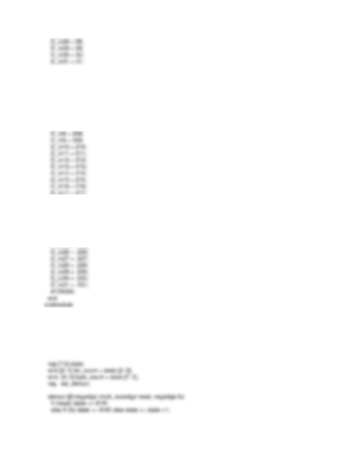
D_in25 = 25;
D_in26 = 26;
D_in27 = 27;
#125000
D_in0 = 200;
D_in1 = 201;
D_in2 = 202;
D_in3 = 203;
D_in4 = 204;
D_in5 = 205;
D_in6 = 206;
D_in7 = 207;
D_in18 = 218;
D_in19 = 219;
D_in20 = 220;
D_in21 = 221;
D_in22 = 222;
D_in23 = 223;
D_in24 = 224;
module Digital_Switch_Control_Unit (
output [4: 0] sel_mux, sel_demux,
output load, load_Data_Register,
input fs,
input clock, reset
);
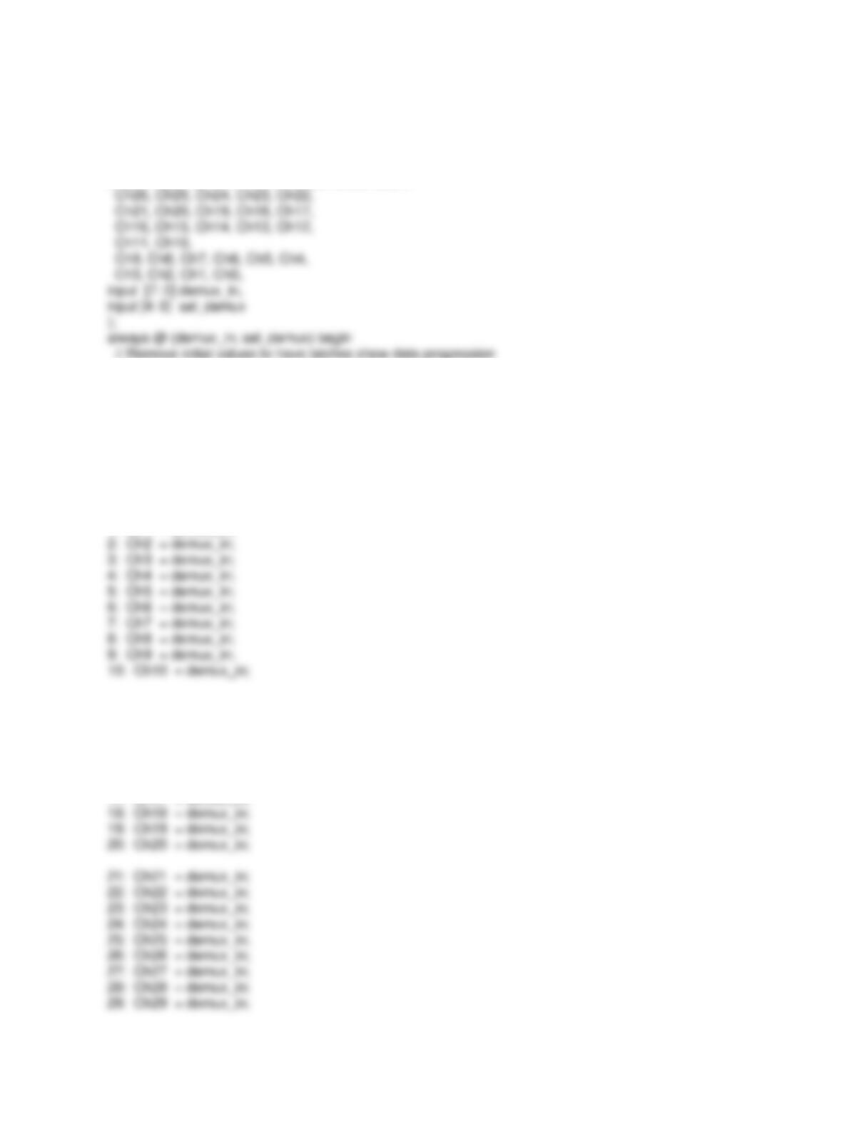
assign load_Data_Register = (state[2:0] == 7);
assign sel_mux = byte_count + 1;
always @(negedge clock) begin sel_demux <= sel_mux-2; end
assign load = (state[2:0] == 0);
endmodule
module Digital_Switch_Demux (
output reg [7: 0] Ch31, Ch30, Ch29, Ch28, Ch27,
/*Ch0 = 0; Ch1 = 0; Ch2 = 0; Ch3 = 0; Ch4 = 0;
Ch5 = 0; Ch6 = 0; Ch7 = 0; Ch8 = 0; Ch9 = 0;
Ch10 = 0; Ch11 = 0; Ch12 = 0; Ch13 = 0; Ch14 = 0;
Ch15 = 0; Ch16 = 0; Ch17 = 0; Ch18 = 0; Ch19 = 0;
Ch20 = 0; Ch21 = 0; Ch22 = 0; Ch23 = 0; Ch24 = 0;
Ch25 = 0; Ch26 = 0; Ch27 = 0; Ch28 = 0; Ch29 = 0;
Ch30 = 0; Ch31 = 0;
*/
case (sel_demux)
0: Ch0 = demux_in;
1: Ch1 = demux_in;
11: Ch11 = demux_in;
12: Ch12 = demux_in;
13: Ch13 = demux_in;
14: Ch14 = demux_in;
15: Ch15 = demux_in;
16: Ch16 = demux_in;
17: Ch17 = demux_in;
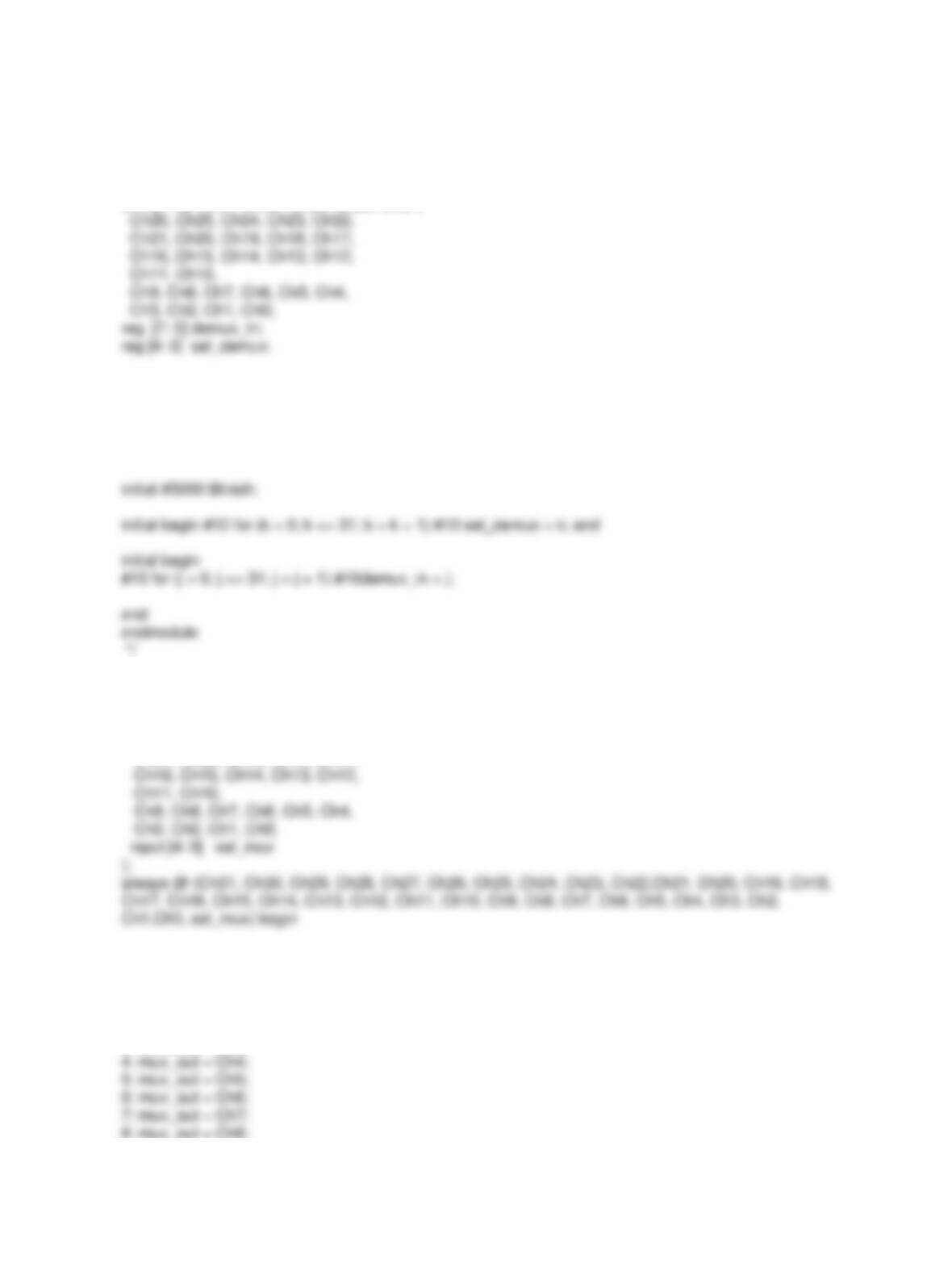
30: Ch30 = demux_in;
31: Ch31 = demux_in;
endcase
end
endmodule
/*
module t_Digital_Switch_Demux ();
wire [7: 0] Ch31, Ch30, Ch29, Ch28, Ch27,
integer j, k;
Digital_Switch_Demux M0 (Ch31, Ch30, Ch29, Ch28, Ch27, Ch26, Ch25, Ch24, Ch23, Ch22,Ch21,
Ch20, Ch19, Ch18, Ch17, Ch16, Ch15, Ch14, Ch13, Ch12, Ch11, Ch10, Ch9, Ch8, Ch7, Ch6, Ch5, Ch4,
Ch3, Ch2, Ch1,Ch0, demux_in, sel_demux);
module Digital_Switch_Mux (
output reg [7: 0] mux_out,
input [7: 0] Ch31, Ch30, Ch29, Ch28, Ch27,
Ch26, Ch25, Ch24, Ch23, Ch22,
Ch21, Ch20, Ch19, Ch18, Ch17,
mux_out = 0;
case (sel_mux)
0: mux_out = Ch0;
1: mux_out = Ch1;
2: mux_out = Ch2;
3: mux_out = Ch3;
14: mux_out = Ch14;
15: mux_out = Ch15;
16: mux_out = Ch16;
17: mux_out = Ch17;
18: mux_out = Ch18;
29: mux_out = Ch29;
30: mux_out = Ch30;
31: mux_out = Ch31;
default mux_out = 8’bx;
endcase
end
endmodule
/*
module t_Digital_Switch_Mux ();
wire [7: 0] mux_out;
reg [7: 0] Ch31, Ch30, Ch29, Ch28, Ch27,
reg [4: 0] sel_mux;
integer k;
Digital_Switch_Mux M0 (mux_out, Ch31, Ch30, Ch29, Ch28, Ch27, Ch26, Ch25, Ch24, Ch23,
Ch22,Ch21, Ch20, Ch19, Ch18, Ch17, Ch16, Ch15, Ch14, Ch13, Ch12, Ch11, Ch10, Ch9, Ch8, Ch7,
Ch6, Ch5, Ch4, Ch3, Ch2, Ch1,Ch0, sel_mux);
initial #5000 $finish;
initial begin
#5
Ch10 = 10;
Ch20 = 20;
Ch21 = 21;
Ch22 = 22;
initial begin
#10 for (k = 0; k <= 31; k = k + 1)
#10 sel_mux = k;
#10 for (k = 31; k >= 0; k = k – 1)
#10 sel_mux = k;
end
endmodule
*/
endmodule
module Digital_Switch_Ser_2_Parallel ();
output reg [7: 0] Par_out;
input Serial_in;
input clock, reset;
/*
module t_Digital_Switch_Ser_2_Parallel ();
wire [7: 0] Par_out;
reg Serial_in;
reg clock, reset;
reg load, shift;
Digital_Switch_Ser_2_Parallel M0 (Par_out, Serial_in, load, shift, clock, reset);
initial forever begin
repeat (16) @ (negedge clock) shift = 1;
repeat (16) @ (negedge clock) shift = 0;
end
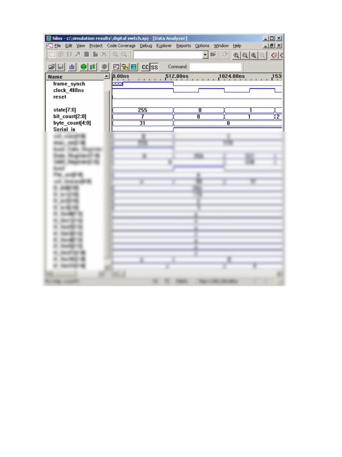
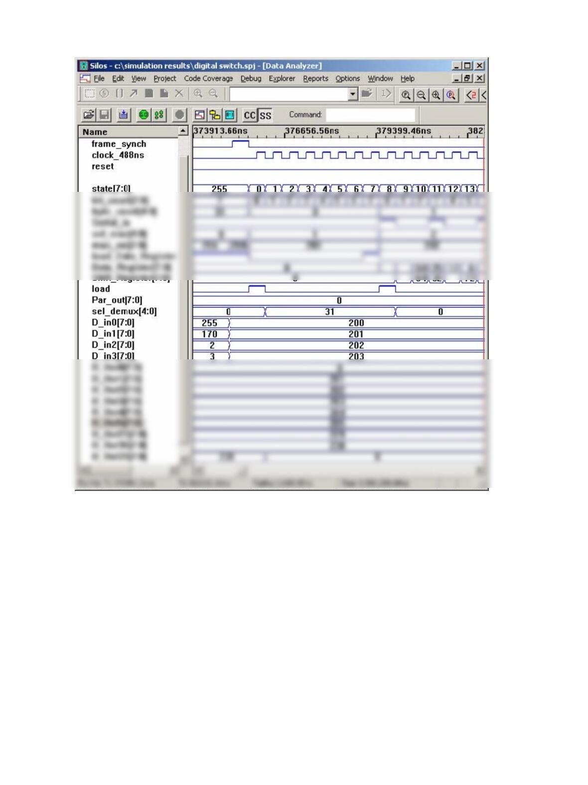
Power-up reset with initial conditions.
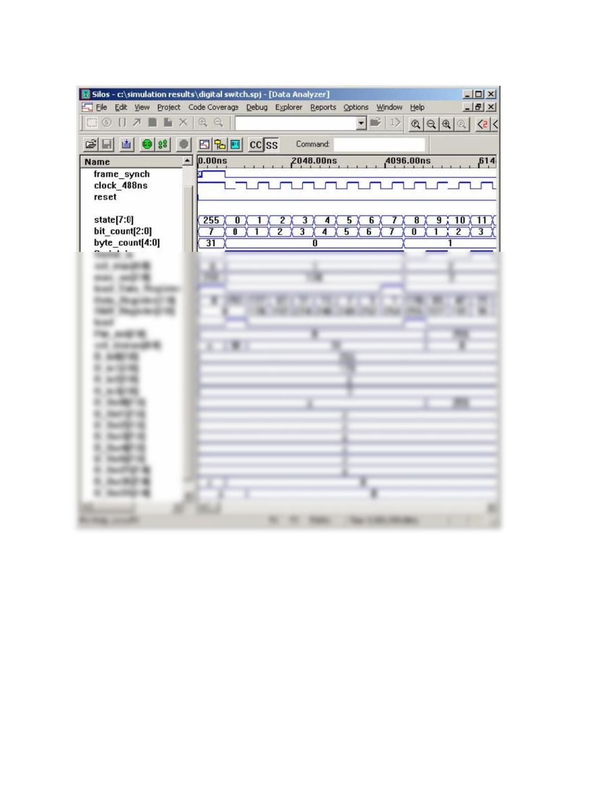
Initial bit sequence of first byte after first synch pulse.
Note location of load_Data_Register and load pulses
Note correct loading of Data_Register, formation of Par_out, and steering of data to D_out7.
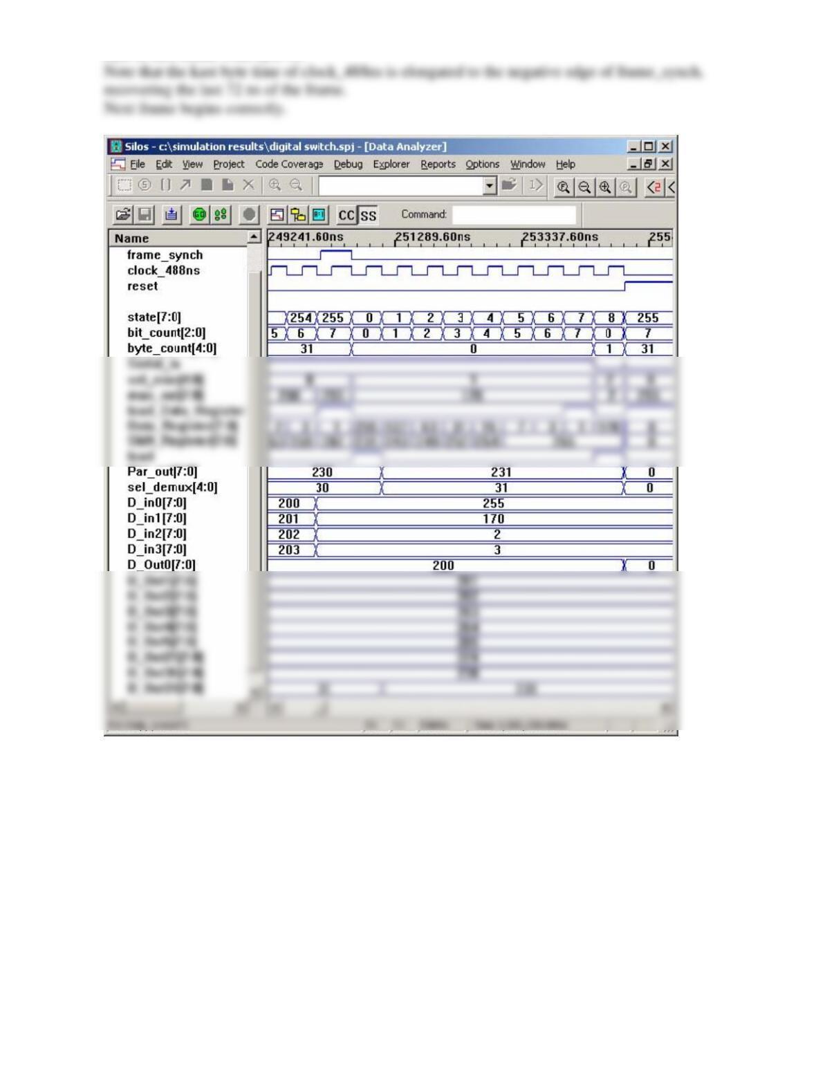
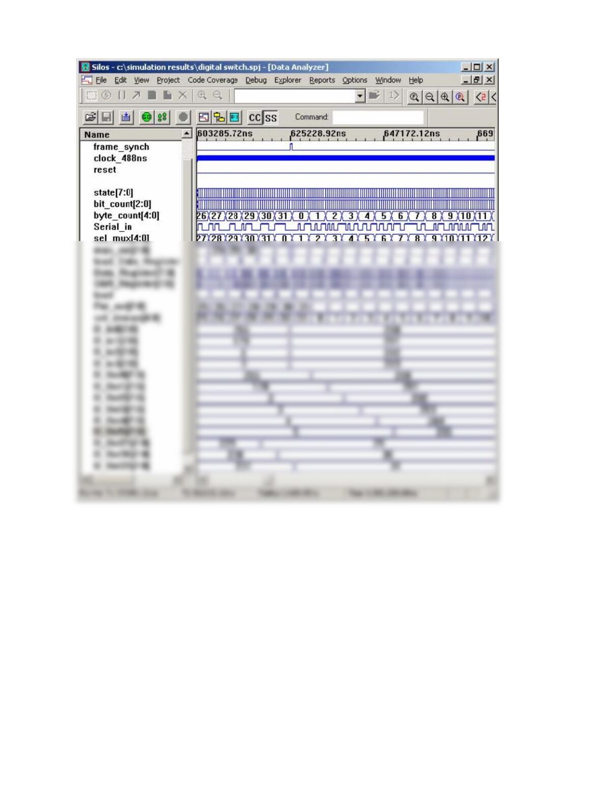
End of first frame with byte 31.
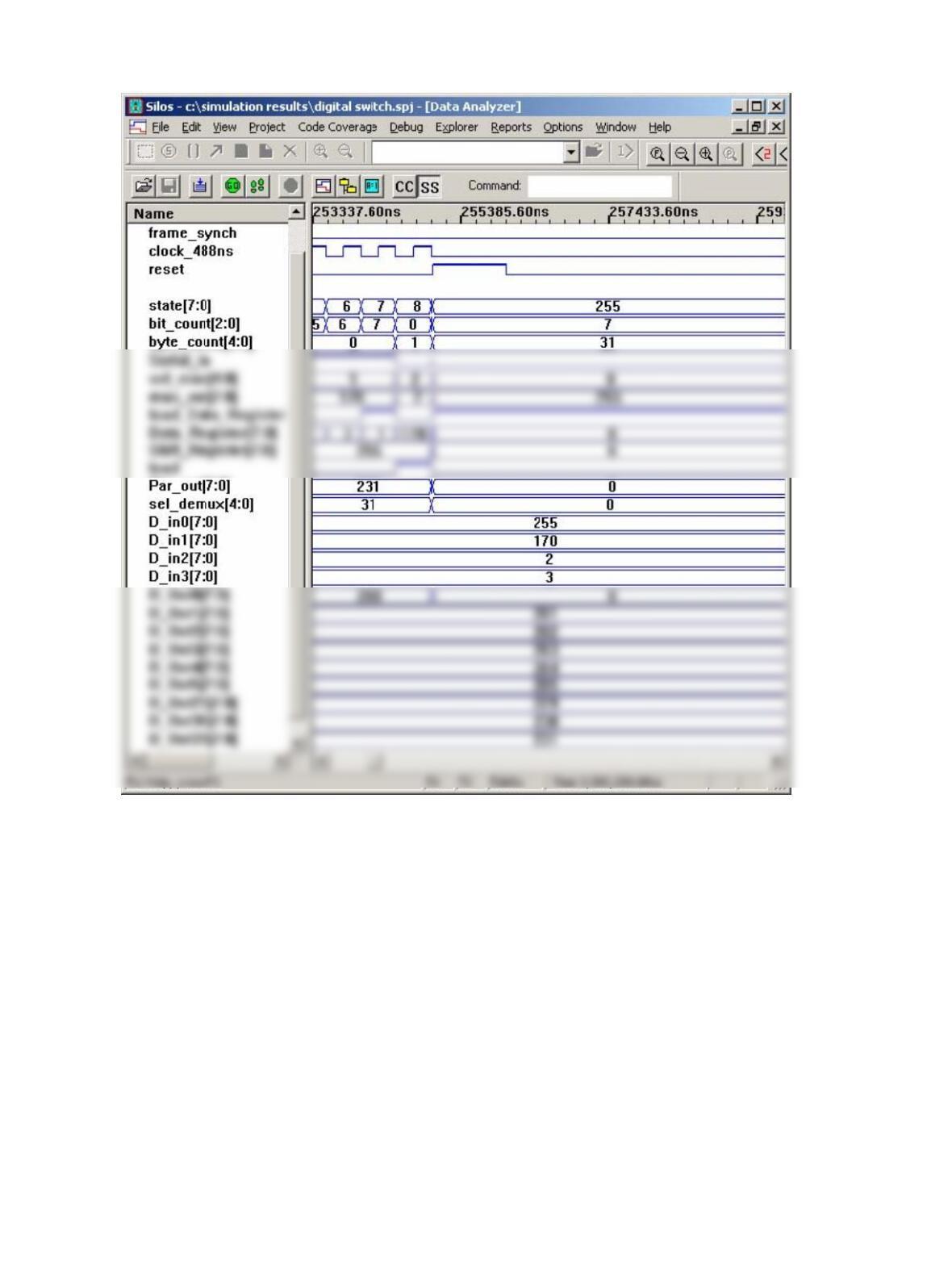
Reset on-the-fly
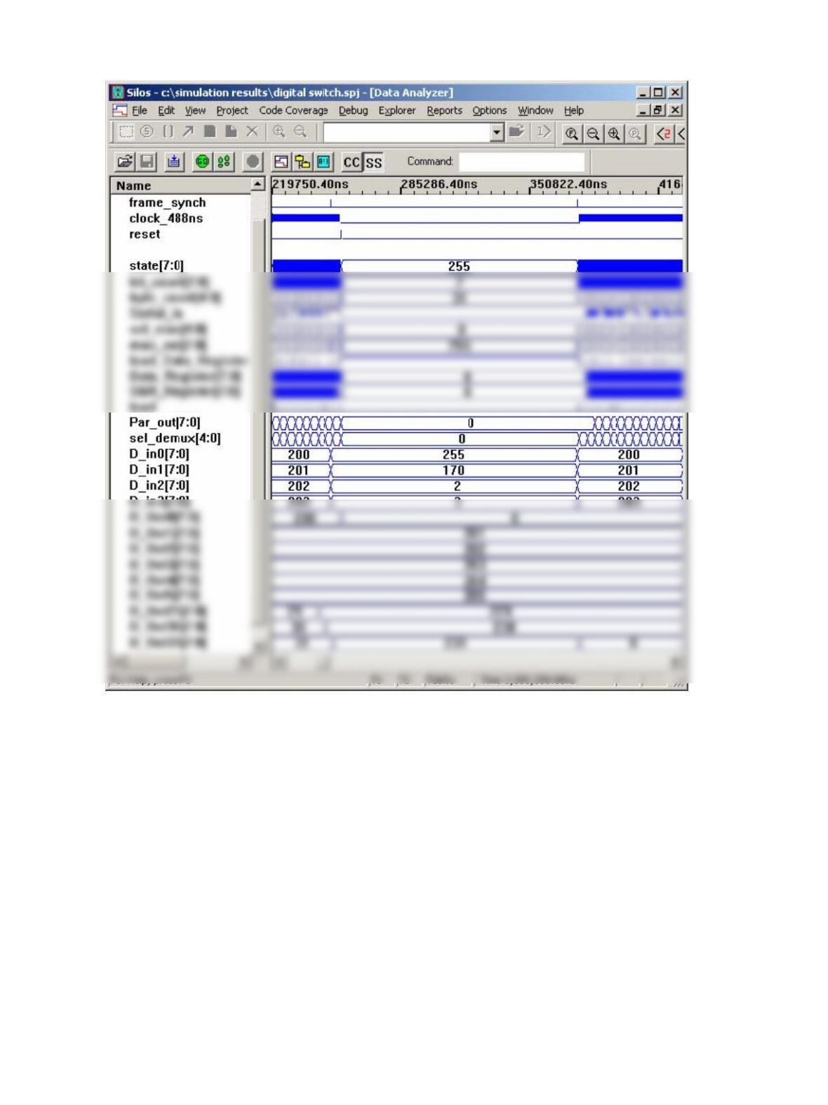
Reset on-the-fly, with wait for the frame_synch pulse to launch the machine.
Recovery from reset on-the-fly.
Alternating patterns of channel.
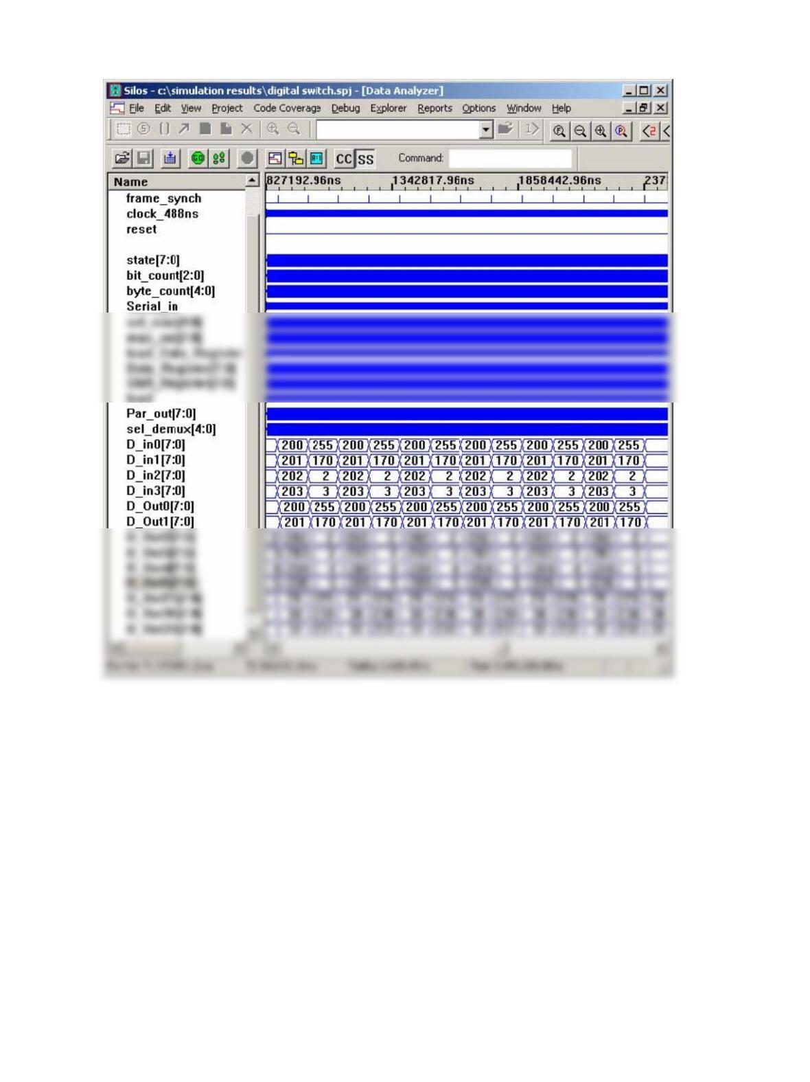
Alternating patterns of data.
Problem 6-22
00
00 01 11 10
1
ab
cd
001
m0m1m3m2
module Prob_6_22 (output f, input a, b, c, d);
always @ (a,b,c,d)
case ({a,b,c,d}
0: f = 1;
1: f = 0;
2: f = 1;
3: f = 0;
4: f = 0;
5: f = 1;
Problem 6-24
A synthesis tool will create combinational logic (feedback-free) from the following Verilog
constructs:

Problem 6-25
A synthesis tool will create a transparent latch from a level-sensitive cyclic behavior having any

Problem 6-26
A synthesis tool will create a cyclic behavior having an edge-triggered sensitivity list.

Problem 6-27
Implement synhronous reset by having thesensitivity list of the edge-sensitive behavior sensitive
to only the clock. The reset condition should be tested in the body of code that follows the