Problem 4-11
c. Use nested for loops to exhaustively generate input patterns to the adder.
for (c_in = 0; c_in <= 1; c_in = c_in + 1)
…

Problem 4-12 (Based on a solution by Marie Anderson)
Test Plan:
For this problem, a testbench was developed to verify a gate-level model of a full adder. The
model which was used for the full adder was that which was given in Example 4.8 (pg 127) of the
text.
Module Code:
module Add_full(output sum, c_out, input a, b, c_in);
wire w1, w2, w3;
Add_half M1(w1, w2, a, b);
Add_half M2(sum, w3, w1, c_in);
or #1 M3(c_out, w2, w3);
endmodule
initial
$monitor($time,,”a=%b, b=%b, c_in=%b, sum=%b, c_out=%b”, a, b,
c_in, sum, c_out);
initial begin
#500 $finish;
end
Reading “adder.v”
Reading “t_adder.v”
sim to 0
Highest level modules (that have been auto-instantiated):
t_Adder
10 total devices.
Linking …
9 nets total: 17 saved and 0 monitored.
67 registers total: 67 saved.
Simulation stopped at the end of time 0.
Ready: sim
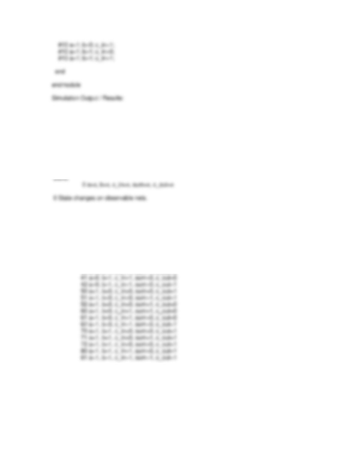
10 a=0, b=0, c_in=0, sum=x, c_out=x
12 a=0, b=0, c_in=0, sum=0, c_out=0
20 a=0, b=0, c_in=1, sum=0, c_out=0
21 a=0, b=0, c_in=1, sum=1, c_out=0
30 a=0, b=1, c_in=0, sum=1, c_out=0
31 a=0, b=1, c_in=0, sum=0, c_out=0
32 a=0, b=1, c_in=0, sum=1, c_out=0
40 a=0, b=1, c_in=1, sum=1, c_out=0
52 State changes on observable nets.
Simulation stopped at the end of time 500.
Ready:

Problem 4-13
Nor-based latch
S = 1; R = 0; sets output to 1
S = 0; R = 0; latches output to 1
Problem 4-14
Assumption: Develop the answer using combinational logic.

Problem 4-15 (Based on a solution by Marie Anderson)
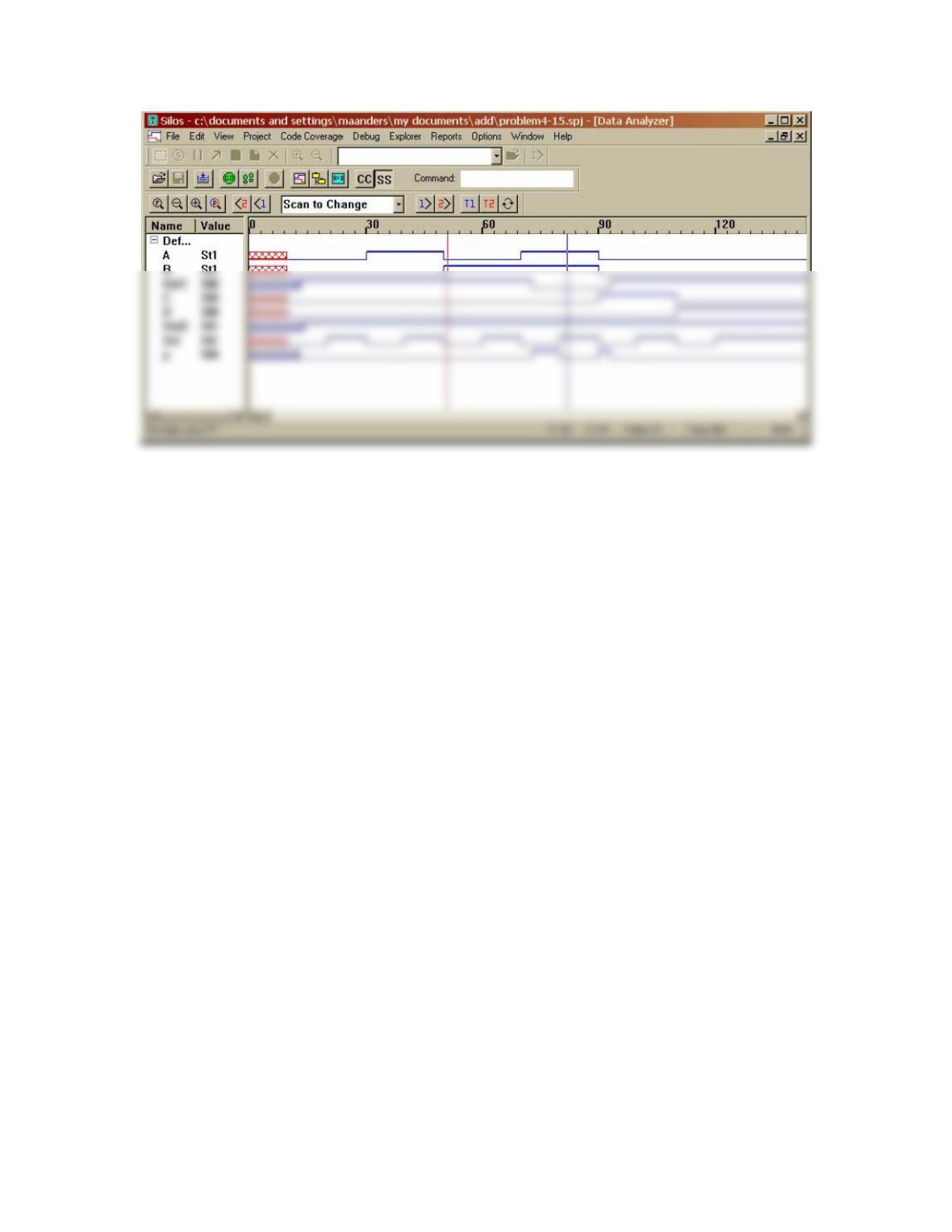
Note: The simulation results shown below are for dimensionless values fo the
propagation delays of the nand gates. To display the effect of the propagations delays
shown in Figure P4-15 insert the following timescale directive at the beginning of the
source file:
`timescale 1ns/10ps
module mux(output y, input y1, y2, Sel);
input y1, y2, Sel;
output y;
module t_delay_mux ();
reg A, B, C, D, Sel;
initial begin
#10 A=0; B=0; C=0; D=0; Sel=0;
#10 A=0; B=0; C=0; D=0; Sel=1;
#10 A=1; B=0; C=0; D=0; Sel=0;
#10 A=1; B=0; C=0; D=0; Sel=1;
#10 A=0; B=1; C=0; D=0; Sel=0;
#10 A=0; B=1; C=0; D=0; Sel=1;
end
endmodule
Simulation Output:
Reading “delay_mux.v”
Reading “t_delay_mux.v”
Reading “mux.v”
0 State changes on observable nets.
Simulation stopped at the end of time 0.
Ready: sim
10 A=0, B=0, C=0, D=0, Sel=0, y=x
13 A=0, B=0, C=0, D=0, Sel=0, y=0
20 A=0, B=0, C=0, D=0, Sel=1, y=0
30 A=1, B=0, C=0, D=0, Sel=0, y=0
40 A=1, B=0, C=0, D=0, Sel=1, y=0
50 A=0, B=1, C=0, D=0, Sel=0, y=0
Problem 4-16
Note: Must use structural models; behavioral models are covered in Ch. 5.
primitive d_prim (output reg q_out, input data, clock, reset);
table
//clk reset data state q_out/next_state
? 1 ? : ? : 0;
? * ? : 0 : 0;
module d_flop_structural (output q_out, q_bar, input data, clock, reset);
d_prim (q_out, data, clock, reset);
not (q_bar, q_out);
endmodule
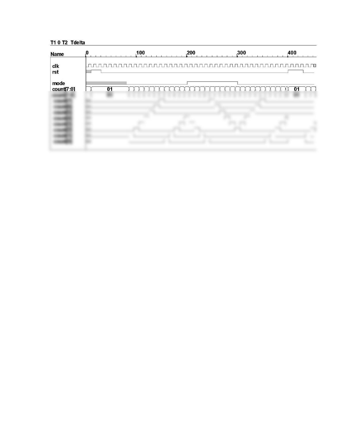
module Problem_4_16 (output reg [7: 0] count, input mode, clk, rst);
// Bidirectional ring counter
// Assume positive-edge sensitive clock; active high reset
wire d0, d1, d2, d3, d4, d5, d6, d7;
mux_2 Mux0 (d0, count[1], count[7], mode);
mux_2 Mux1 (d0, count[2], count[0], mode);
mux_2 Mux2 (d0, count[3], count[1], mode);
d_flop M6 (count[6], d6, clk, 1’b0, rst);
d_flop M7 (count[7], d7, clk, 1’b0, rst);
endmodule
/*
//For comparison, a behavioral model is given below.
module Problem_4_16 (count, mode, clk, rst);
module t_Problem_4_16 ();
wire [7: 0] count;
reg mode; // mode = 0 for left, mode = 1 for right
reg clk, rst;
Problem_4_16 M0 (count, mode, clk, rst);
Problem 4-17
Note: The model must be a structural model. The logic of the counter will require four flip-flops
having the state transition table given below:
q3 q2 q1 q0 q3+ q2+ q1+ q0+
0 0 0 0 0 0 0 1
0 0 0 1 0 0 1 0
0 0 1 0 0 0 1 1
0 0 1 1 0 1 0 0
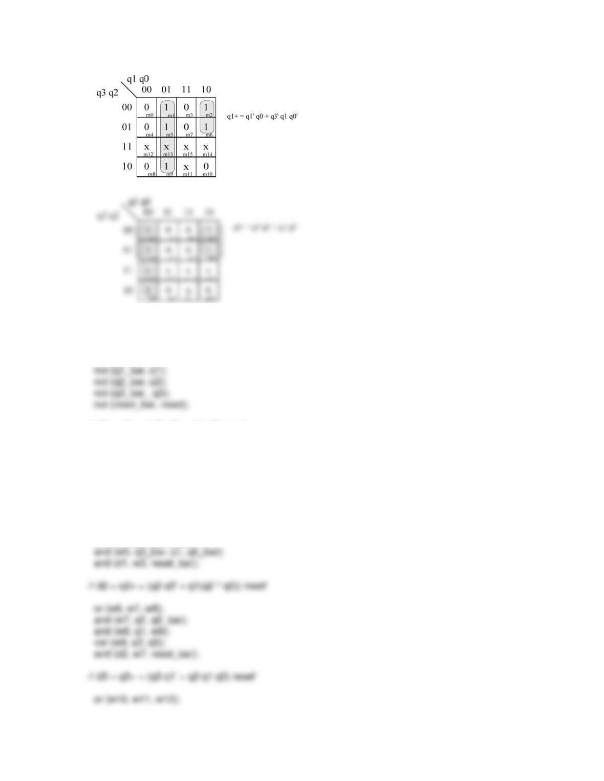
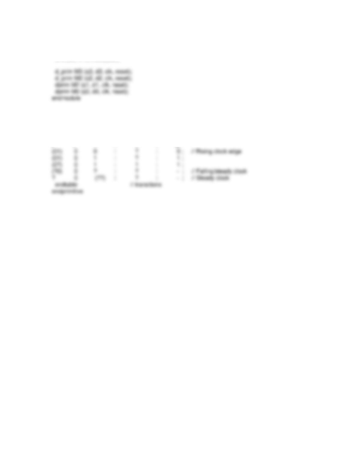
The next-state equations must be combined with the reset conditoon:
module Prob_4_17 (output reg q3, q2, q1, q0, input clk, reset);
not (q0_bar, q0);
// d0 = q0+ = (q3′ q0′ + q1′ q0′) reset’
or (w0, w1, w2);
and (w1, q3_bar, q0_bar);
and (w2, q1_bar, q0_bar);
and (d0, w0, reset_bar);
// d1 = q1+ = (q1′ q0 + q3′ q1 q0′) reset’
or (w3, w4, w5);
and (w4, q1_bar, q0);
and (w10, q3, q1_bar);
and (w11, q2, q1, q0);
and (d3, w10, reset_bar);
primitive d_prim (output reg q_out, input data, clock, reset);
table
//clk reset data state q_out/next_state
? 1 ? : ? : 0;
? * ? : 0 : 0;
r 1 ? : ? : 0;
Problem 4-19
Note: The model must be a structural model (Behavioral modesl are presetned in Chapter 5).
primitive T_prim (output reg Q, input clock, rst_b, toggle);
table
// clk rst_b toggle state Q/next_state
? 0 ? : ? : 1 ;
? 1 1 : ? : – ;
(01) 1 0 : ? : – ; // Rising clock edge
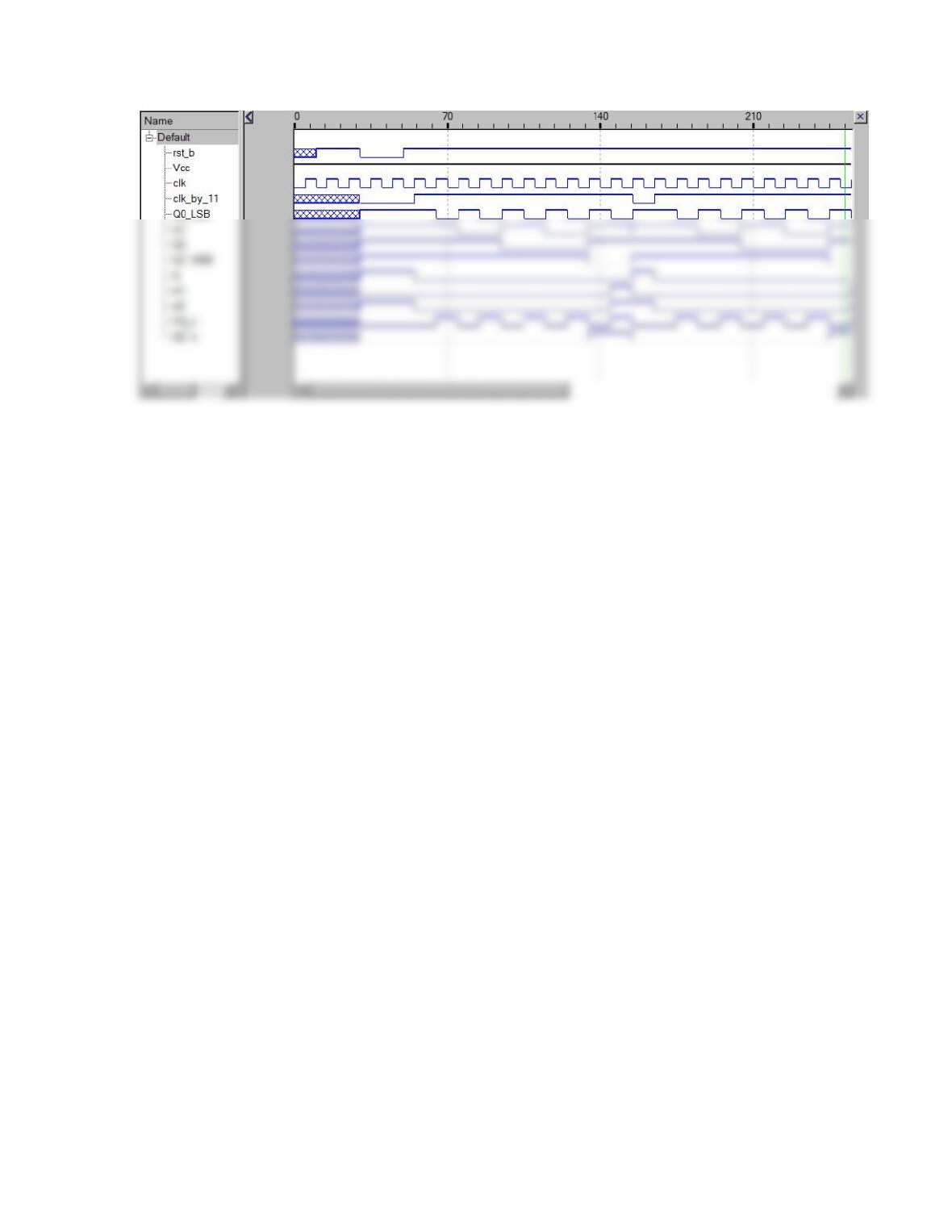
module Divide_by_11 (output clk_by_11, input clk, rst_b, Vcc);
wire Q0_LSB, Q1, Q2, Q3_MSB, w1, w2;
T_prim T0 (Q0_LSB, clk, clk_by_11, Vcc);
T_prim T1 (Q1, Q0_LSB, clk_by_11, Vcc);
T_prim T2 (Q2, Q1, clk_by_11, Vcc);
T_prim T3 (Q3_MSB, Q2, clk_by_11, Vcc);