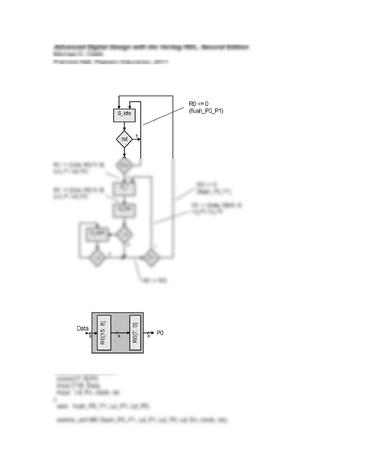
Problem 5-30
module Problem_5_30 (
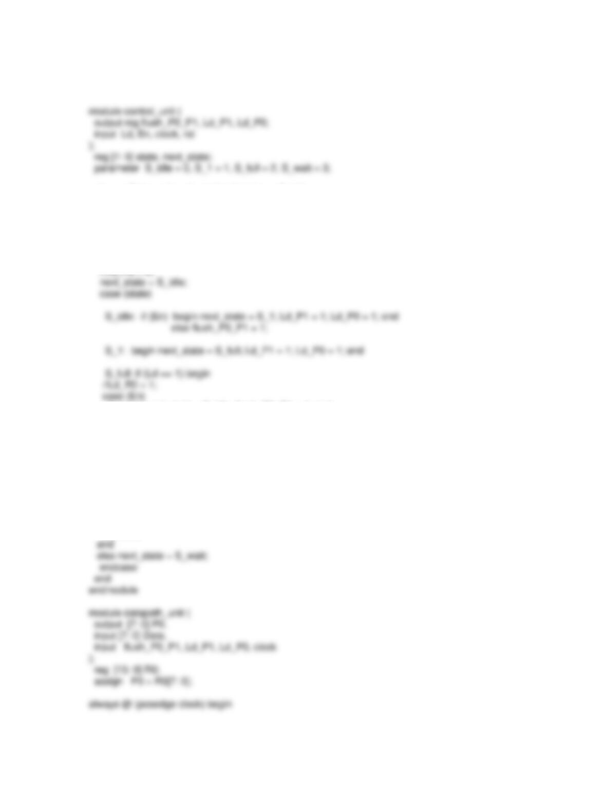
datapath_unit M1 (P0, Data, flush_P0_P1, Ld_P1, Ld_P0, clock);
endmodule
always @ (posedge clock) if (rst) state <= S_idle;
else state <= next_state;
always @ (state, Ld, En) begin
flush_P0_P1 = 0;
Ld_P1 = 0;
Ld_P0 = 0;
//Ld_R0 = 0;
0: begin next_state = S_idle; flush_P0_P1 = 1; end
1: begin next_state = S_1; Ld_P1 = 1; Ld_P0 = 1; end
endcase
end
else next_state = S_wait;
S_wait: if (Ld == 1) begin
//Ld_R0 = 1;
case (En)
0: begin next_state = S_idle; flush_P0_P1 = 1; end
1: begin next_state = S_1; Ld_P1 = 1; Ld_P0 = 1; end
endcase
if (flush_P0_P1) begin R0 <= {Data, R0[15: 0]}; end
if (Ld_P1) R0[15: 7] <= Data;
if (Ld_P0) R0[7: 0] <= R0[15: 8];
end
endmodule
Problem_5_30 M0 (P0, Data, Ld, En, clock, rst);
initial #700 $finish;
initial begin clock = 0; forever #5 clock = ~clock; end
initial fork
Data = 8’haa;
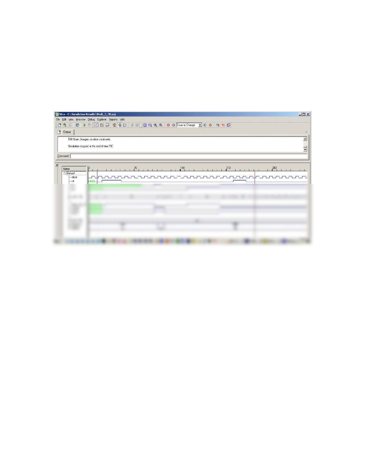
#10 rst = 0; // Power-up reset
#20 rst = 1;
#50 rst = 0;
Problem 5-31
The machine described by the ASM in figure 5-41 6 states. If the unused states are
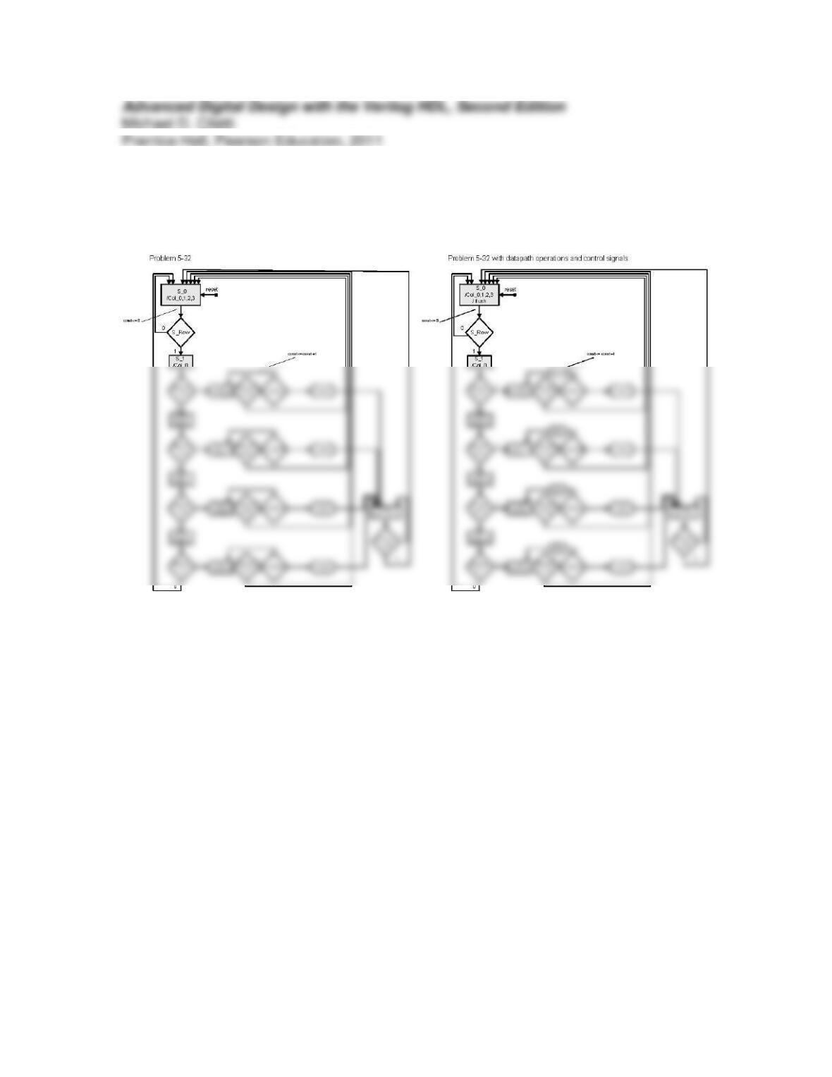
Problem 5-32
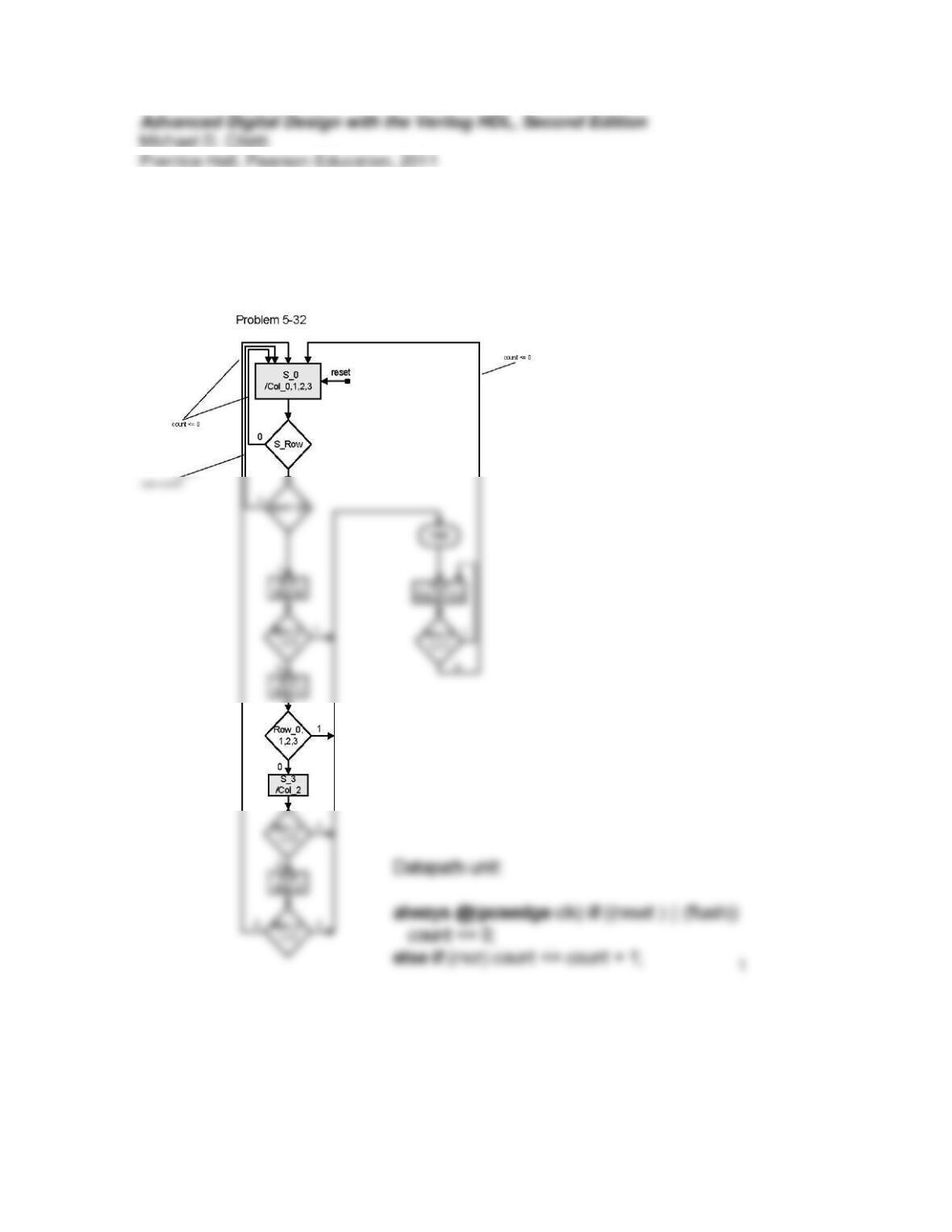
Problem 5-32 Alternative solution
1
Problem 5-33
module Clock_Prog (output reg clock);
parameter Latency = 100;
parameter Offset = 75;
parameter Pulse_Width = 25;
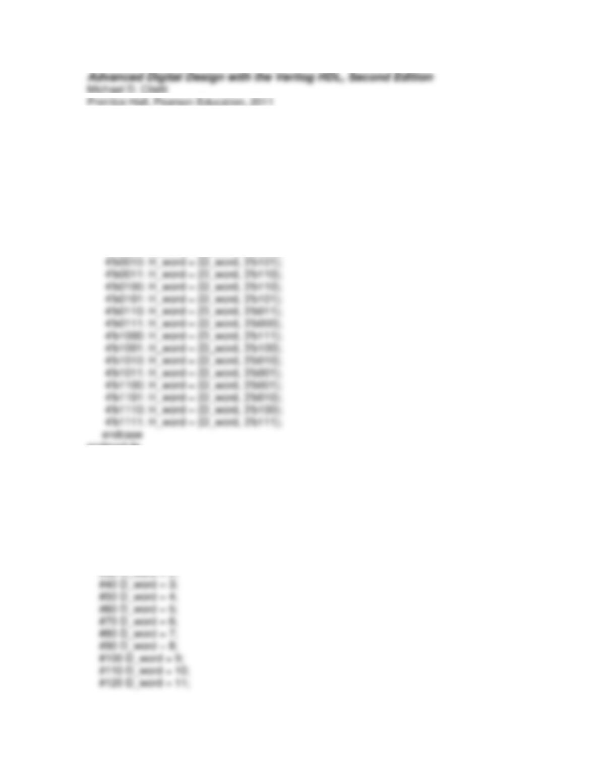
module t_Clock_Prog ();
wire clock;
initial #100 $finish;
Clock_Prog M1 (clk);
endmodule
Problem 5-35 (a)
module Prob_5_35a_Hamming_Encoder (
output reg [6:0] H_word,
input [3: 0] D_word
);
always @ (D_word)
case (D_word)
4’b0000: H_word = {D_word, 3’b000};
4’b0001: H_word = {D_word, 3’b011};
endmodule
(b)
module t_Prob_5_35a_Hamming_Encoder ()
wire [6:0] H_word;
reg [3: 0] D_word);
initial $500 $finish;
initial fork
#10 D_word = 0;
#20 D_word = 1;
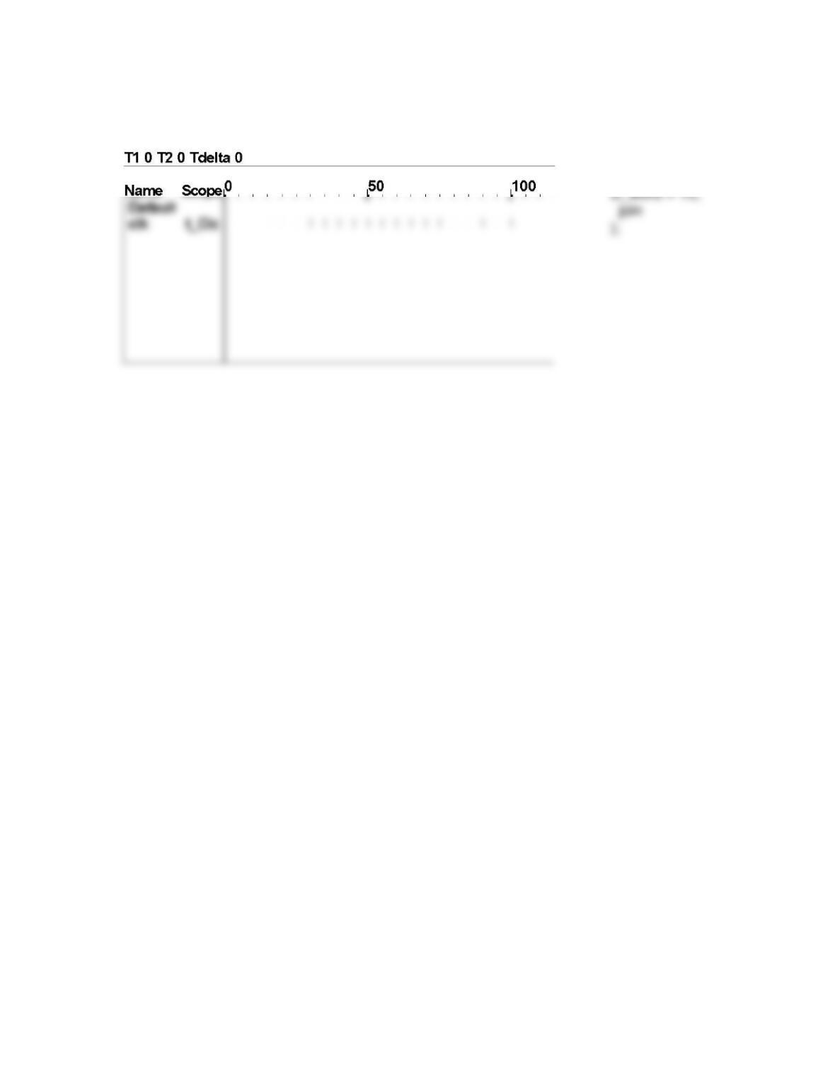
#130 D_word = 12;
#140 D_word = 13;
#150
D_word = 14;
#160
Answer: Some of you might be experiencing difficulty in simulating the gate level
timing violation and assert an x on their output. This locks the machine in the x state. To
Question: In working problems 1, 2, 3 in Chapter 6 you may notice glitches in the
waveform of the output of the synthesized Moore machines. What is the cause?
Question: When I compare a behavioral model and a gate-level model I find that the
gate-level model does match. In fact, it produces waveforms that are x. Why?
Problem 5-36
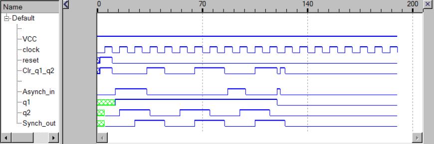
The following models can be used to test and synthesize the synchronizer of Figure 5-38.
Replace the generic cells with parts from a standard cell library. Note that the pulse that
is narrower than the period of the clock has no effect.
module D_flop(output reg Q, input D, clock, Clr);
always @ (posedge clock)
if(Clr) Q <= 0;
else Q <= D;
endmodule
module test_Prob_5_36();
wire Synch_out;
reg Asynch_in, clock, reset, VCC;
Problem 5-37
N
ote: The model of Latch_Rbar_CA in Example 5.8 should have
assign q_out = (rst_b == 1′b0) ? 0 : enable ? data_in : q_out;
Latch_Rbar_S_CA M0( q_out, data_in, enable, reset_bar, set);
initial #100 $finish;
initial fork
#5 reset_bar = 0;
#25 reset_bar = 1;
#73 reset_bar = 0;
#85 reset_bar = 1;
begin data_in = 0; forever #5 data_in = ~data_in; end
join
endmodule
Problem 5-38
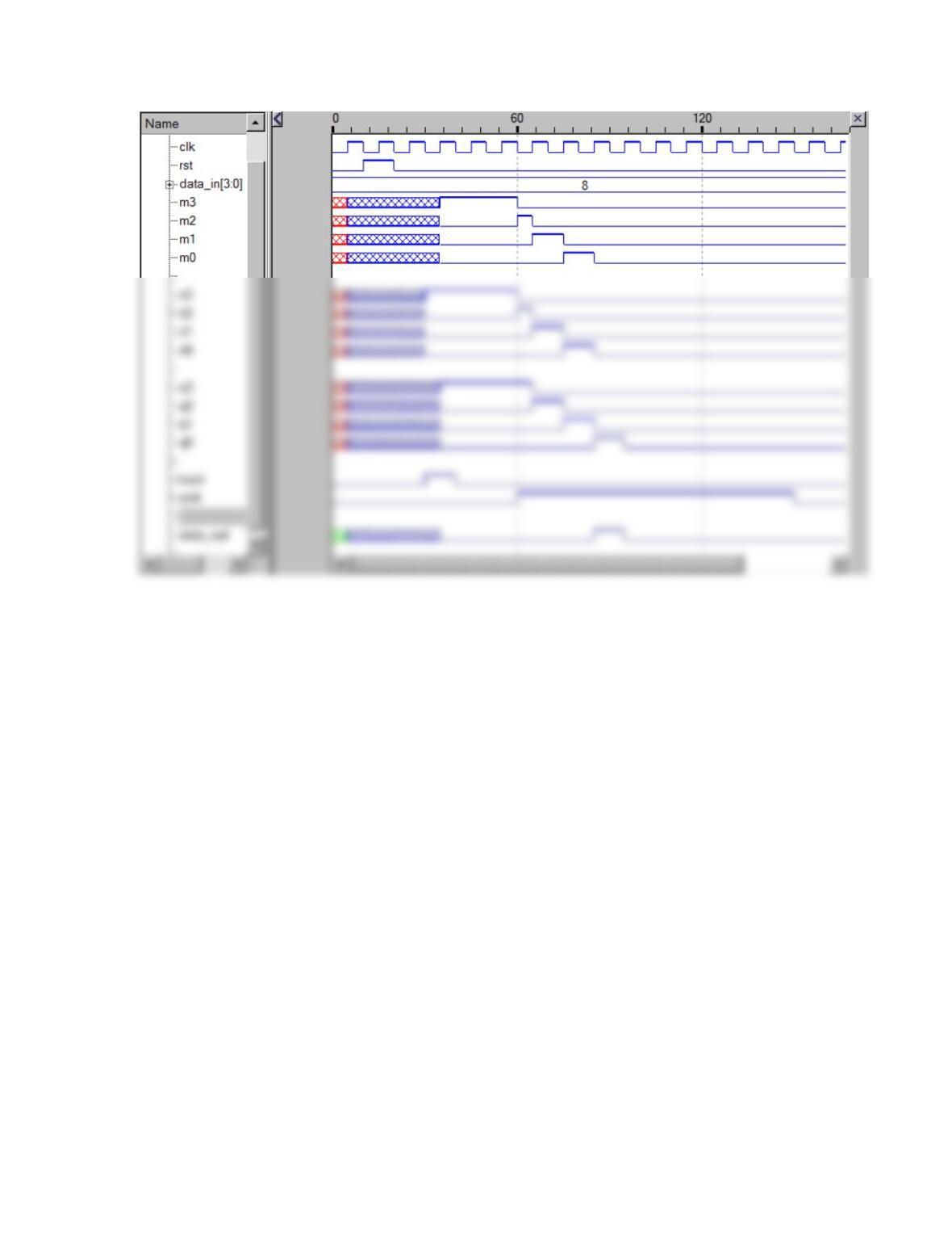
The structure shown below implements the shifting and loading operations. If load is
asserted, the flip-flop receives data[3:0]. Otherwise each receives the output of the mux
connected to its data line. The input to that mux is either the re-circulated output (shift =
0) or the output of the previous stage (shift = 1).
module Prob_5_38 (output data_out, input [3:0] data_in, input load, shift, clk, rst);
wire q3, q2, q1, q0;
assign data_out = q0;
wire m0, m1, m2, m3;
supply0 GND;
mux M0a(d0, load, m0, data_in[0]);
mux M0b(m0, shift, q0, q1);
d_prim1 M0(q0, clk, d0);
output reg q_out,
input clock, data
);
table
// clk data state q_out/next_state
module test_Prob_5_38 ();
wire data_out;
reg [3:0] data_in;
reg load, shift, clk, rst;
Prob_5_38 M0( data_out, data_in, load, shift, clk, rst);
Problem 5_39
module Prob_5_39 # (parameter left = 1’b0, right = 1’b1)(
output reg [7:0] Data_out,
input [7:0] Data_in,
input [2:0] step,
input LR,
if (LR == left)
case(step)
0: Data_out <= Data_out;
1: Data_out <= {Data_out[6:0], Data_out[7]};
if(LR == right)
case(step)
0: Data_out <= Data_out;
1: Data_out <= {Data_out[0], Data_out[7:1]};
endmodule
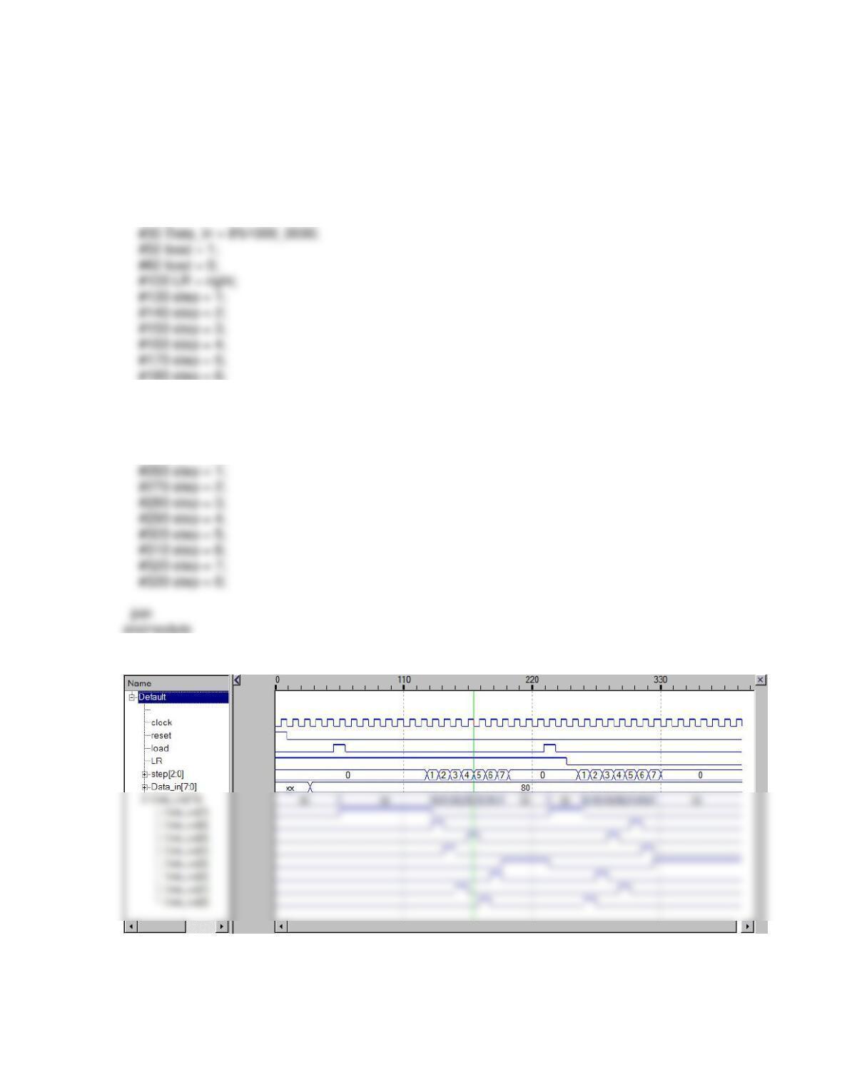
module test_Prob_5_39 #(parameter left = 1’b0, right = 1’b1)();
wire [7:0] Data_out;
reg [7:0] Data_in;
initial fork
reset = 1;
LR = right;
load = 0;
step = 0;
#10 reset = 0;
#190 step = 7;
#200 step = 0;
#230 load = 1;
#240 load = 0;
#250 LR = left;