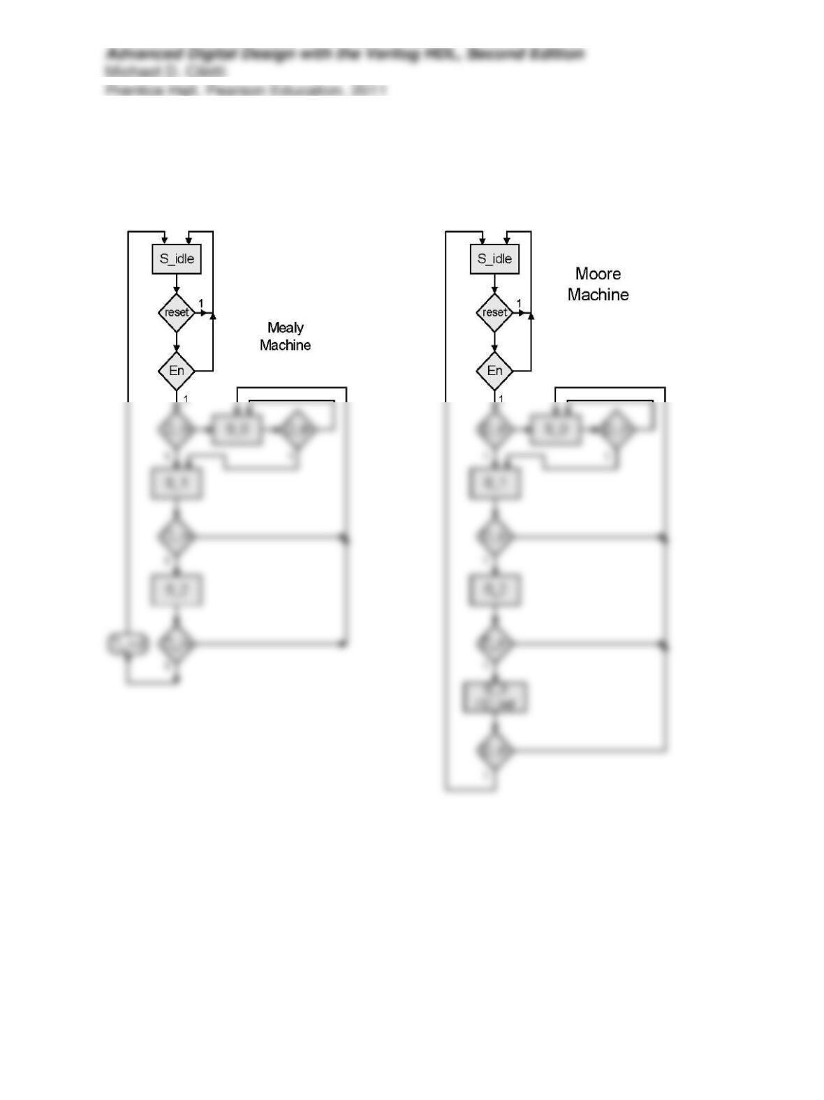
Problem 6-4
Resetting machines:
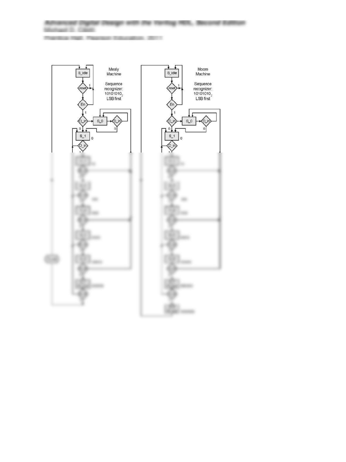
Problem 6-5
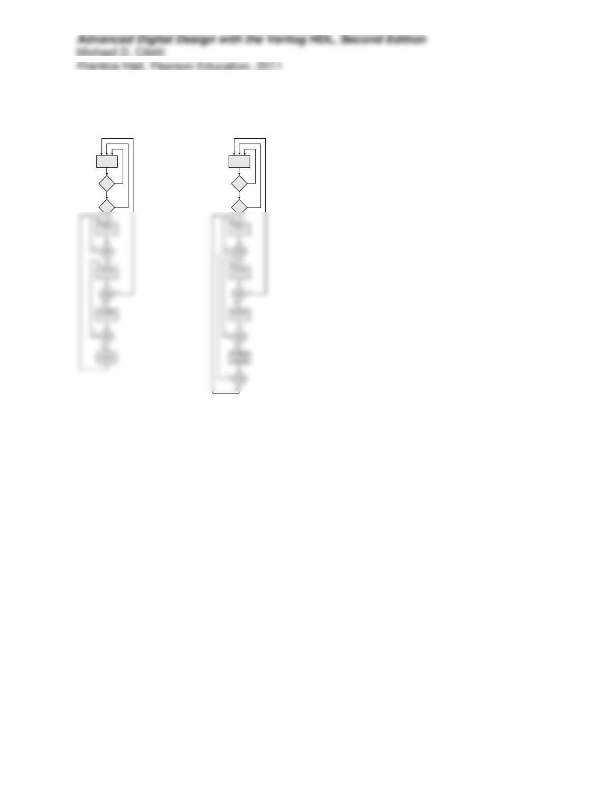
Problem 6-6
1
rst
S_idle
1
bit
1
rst
S_idle
1
bit
Mealy Machine Moore Machine
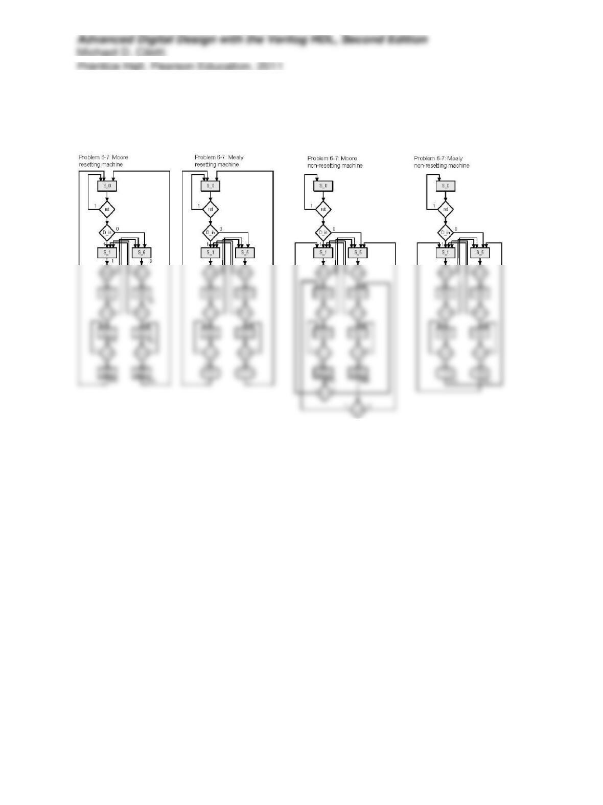
Problem 6-7
Solution for resetting machine is not required, but is shown here for comparison.
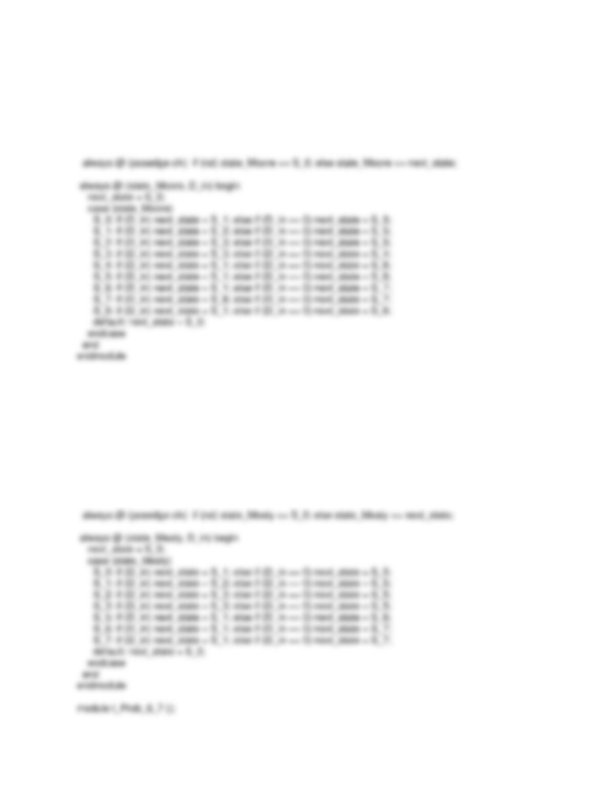
module Prob_6_7_Moore (
// Moore nonresetting sequence detector
output Detect_Moore,
input D_in, clk, rst
);
parameter S_0 = 0, S_1 = 1, S_2 = 2, S_3 = 3, S_4 = 4;
parameter S_5 = 5, S_6 = 6, S_7 = 7, S_8 = 8;
reg [3: 0] state_Moore, next_state;
assign Detect_Moore = ((state_Moore == S_4) || (state_Moore == S_8));
module Prob_6_7_Mealy (
// Mealy nonresetting sequence detector
output Detect_Mealy,
input D_in, clk, rst
);
parameter S_0 = 0, S_1 = 1, S_2 = 2, S_3 = 3;
parameter S_5 = 5, S_6 = 6, S_7 = 7;
reg [2: 0] state_Mealy, next_state;
assign Detect_Mealy = (((state_Mealy == S_3)&&(D_in == 0))
|| ((state_Mealy == S_7)&&(D_in ==1)));
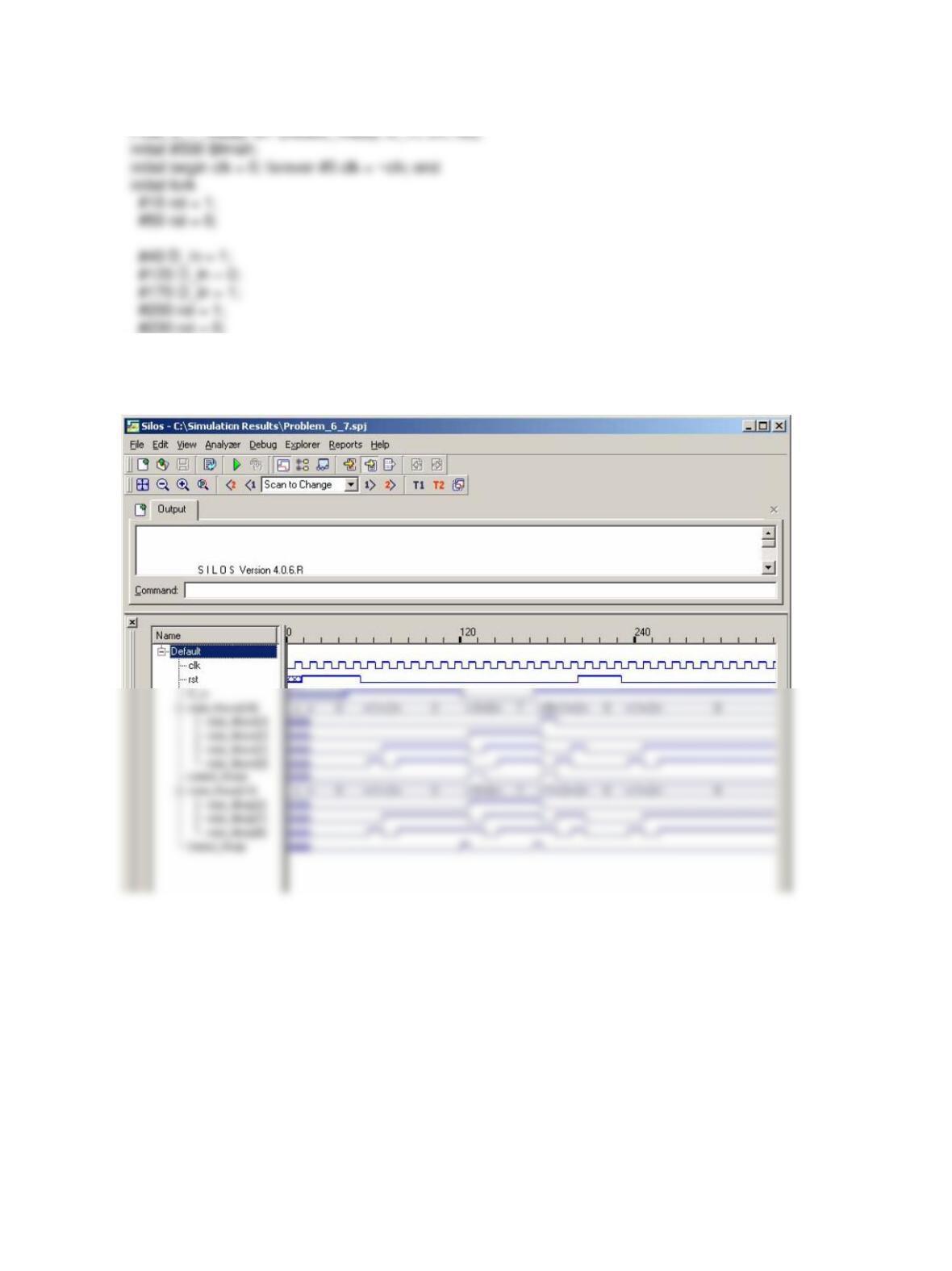
wire Detect_Moore, Detect_Mealy;
reg D_in, clk, rst;
Prob_6_7_Moore M0 (Detect_Moore, D_in, clk, rst);
join
endmodule
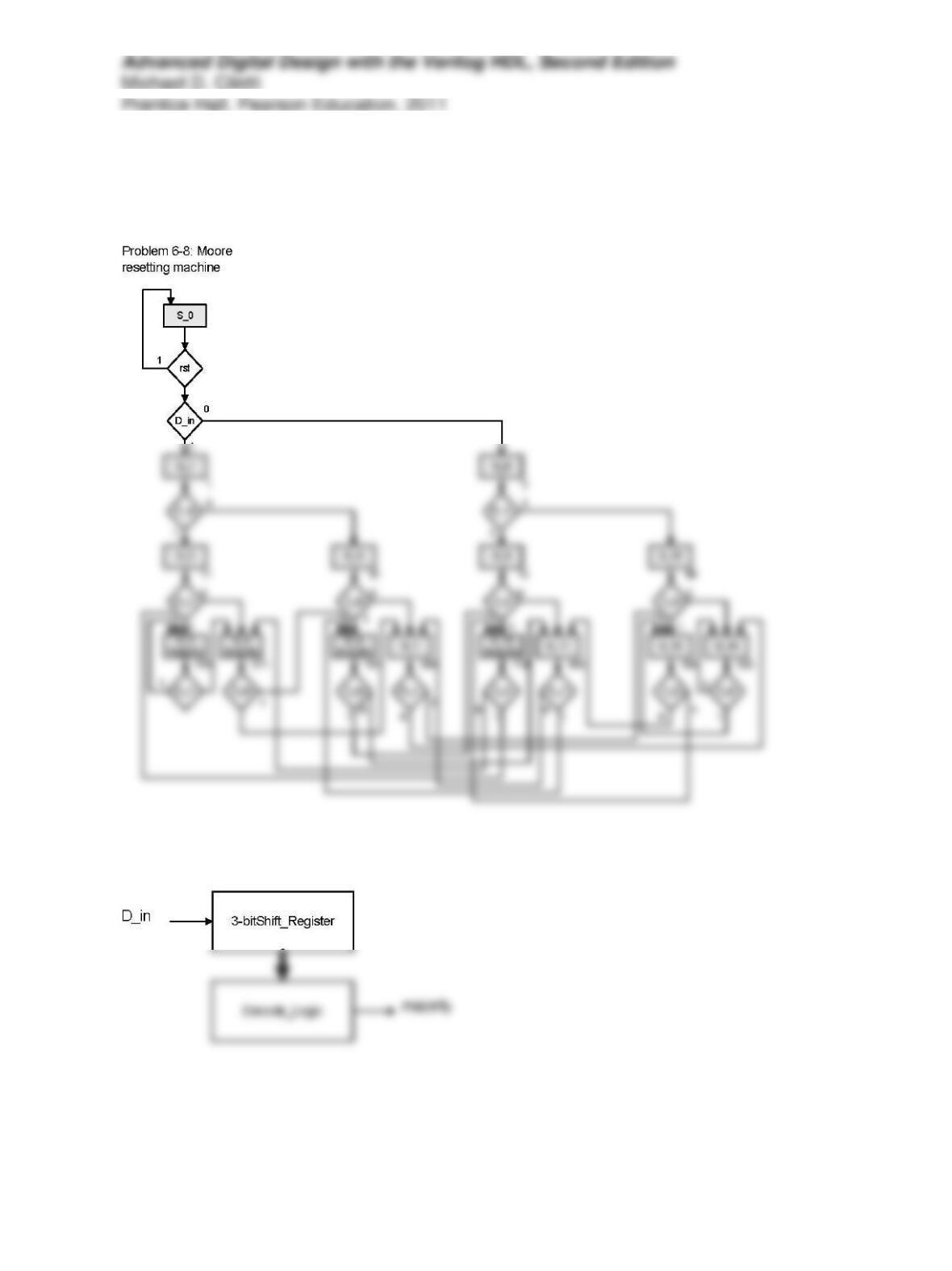
Problem 6-8
For simplicity, the machine is realized as a state machine with an output that asserts the majority
function.
A simple hardware realization (alternative).
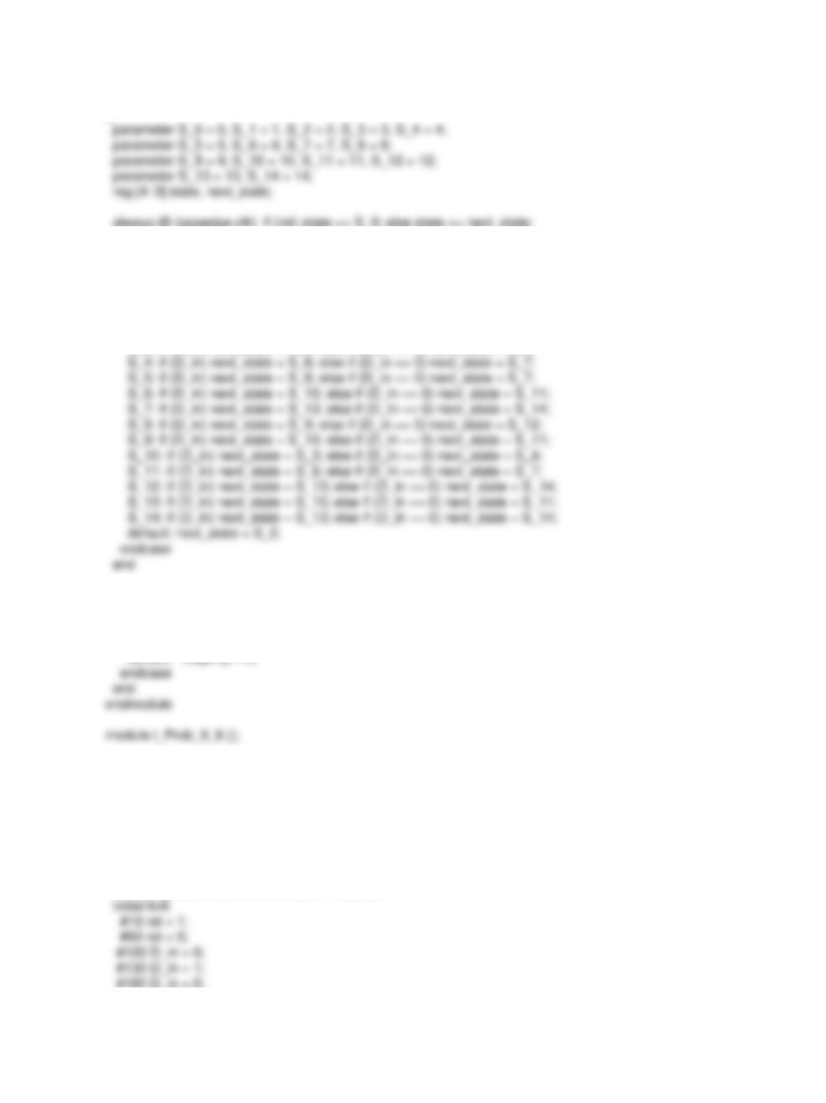
module Prob_6_8 (
// majority function
output reg majority,
input D_in, clk, rst
);
always @ (posedge clk) if (rst) state <= S_0; else state <= next_state;
always @ (state, D_in) begin
next_state = S_0;
case (state)
S_0: if (D_in) next_state = S_1; else if (D_in == 0) next_state = S_8;
S_1: if (D_in) next_state = S_2; else if (D_in == 0) next_state = S_5;
S_2: if (D_in) next_state = S_3; else if (D_in == 0) next_state = S_4;
S_3: if (D_in) next_state = S_3; else if (D_in == 0) next_state = S_4;
always @ (state, D_in) begin
majority = 0;
case (state)
S_3, S_4, S_6, S_10: majority = 1;
default: majority = 0;
wire majority;
reg D_in, clk, rst;
reg [2:0] Data_Reg;
// View the data stream:
always @ (posedge clk) Data_Reg <= {D_in,Data_Reg[2: 1]};
Prob_6_8 M0 (majority, D_in, clk, rst);
initial #500 $finish;
initial begin clk = 0; forever #5 clk = ~clk; end
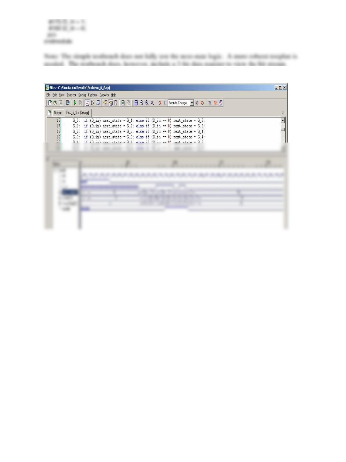
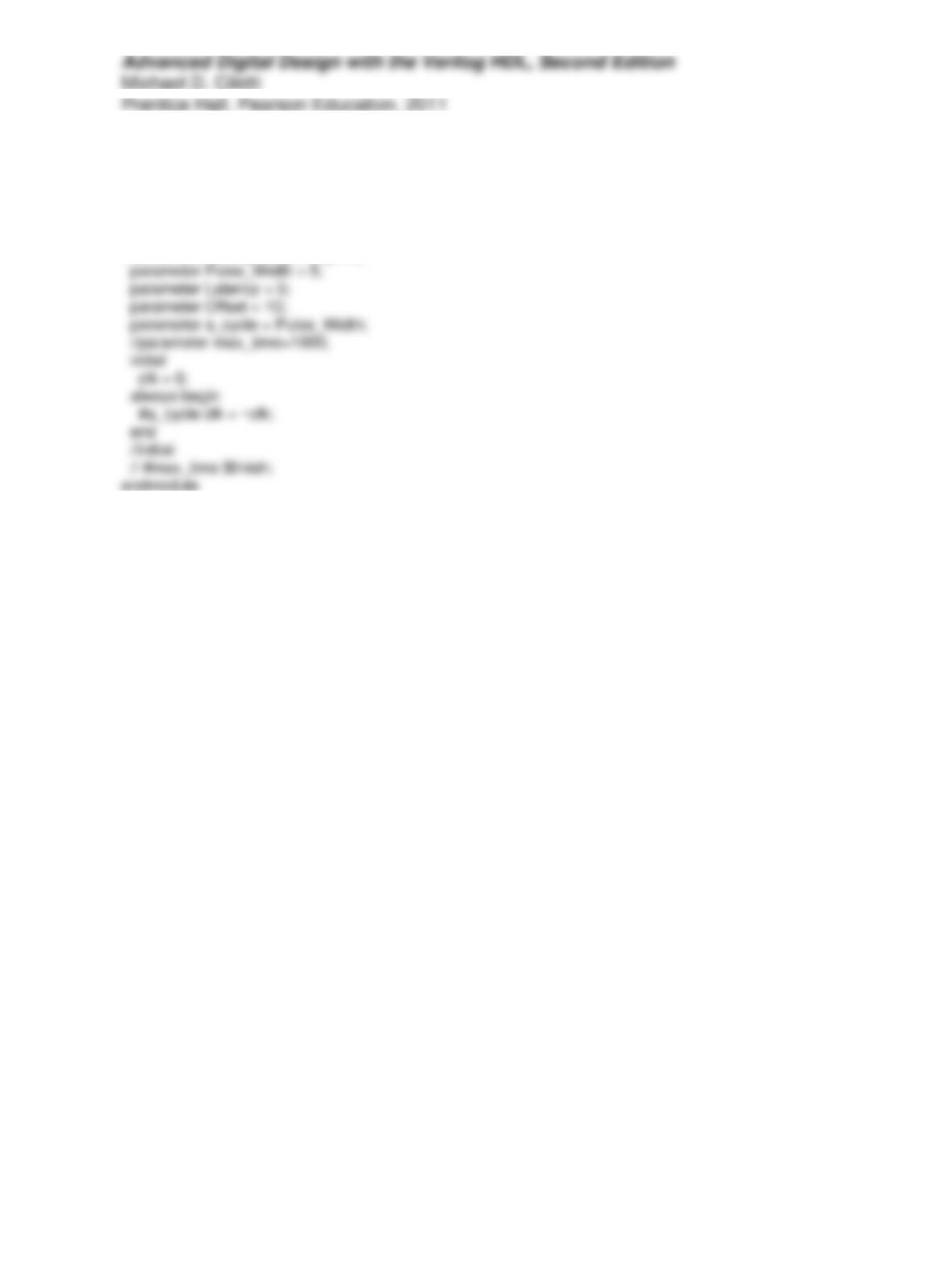
Problem 6-9
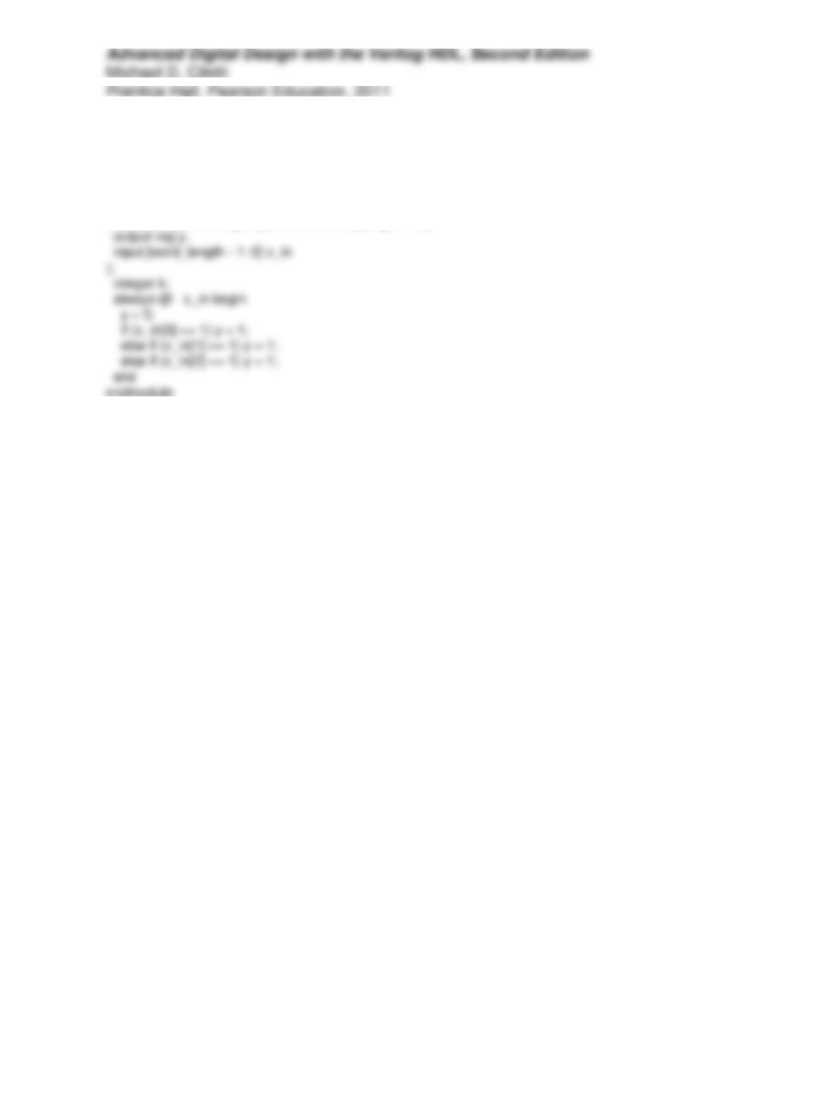
The model has syntax errors that will prevent its compilation. Pulse_Width, Latency, and Offset
cannot be declared inputs and declared parameters. A correct model is given below.
module clock_Prog (output reg clk);
Problem 6-10
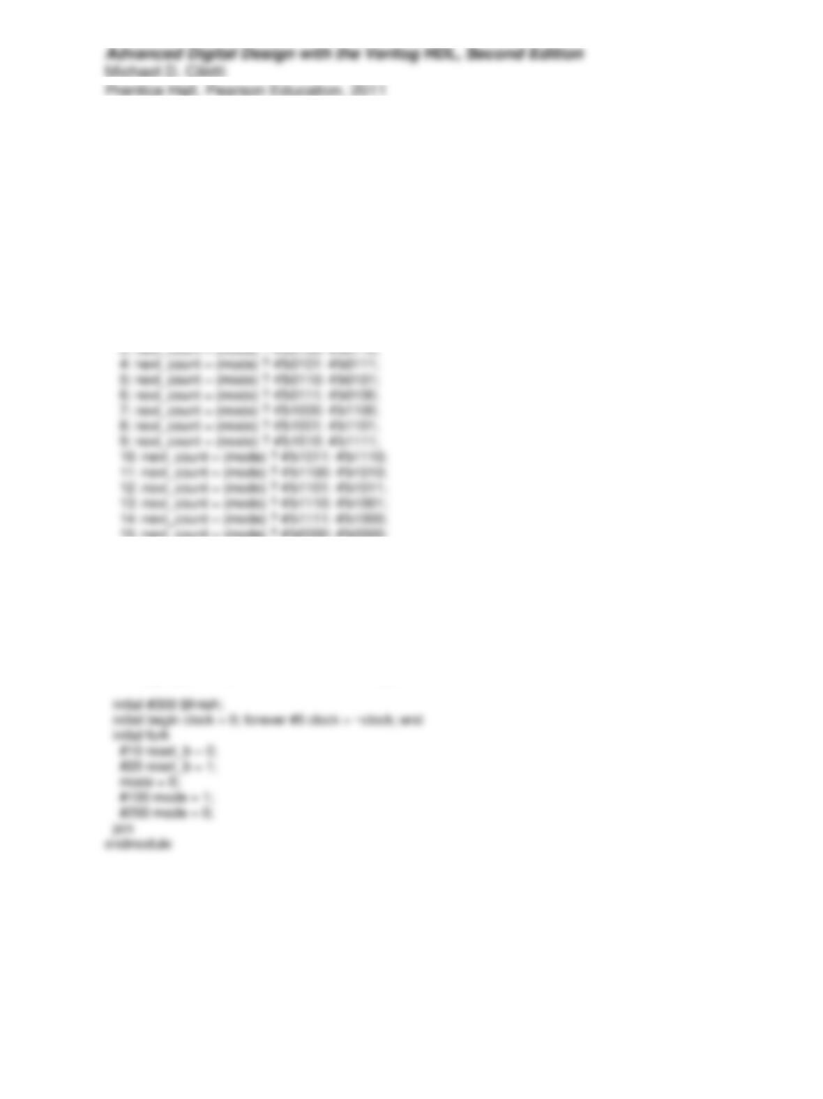
The if statement in the level-sensitive cyclic behavior does not completely decode the bits of
x_in (missing x_in[3] explicitly or implicitly). Therefore, a synthesis tool will create a latch.
moduleor4_something # (parameter word_length = 4)(
Problem 6-16
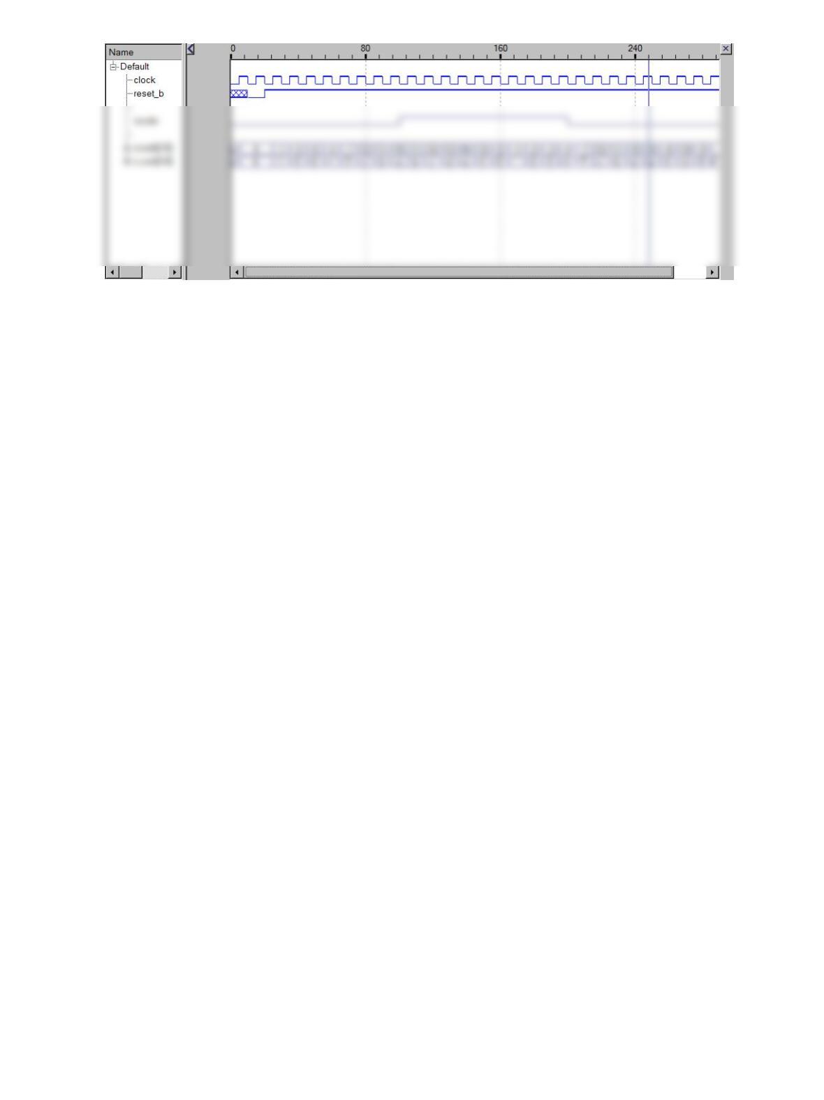
module count_gray_bin (output reg [3:0] count, input mode, clock, reset_b);
reg [3:0] next_count;
always @ (posedge clock)
if (reset_b == 0) count <= 0;
else count <= next_count;
always @ (count, mode) begin
next_count = 0;
case (count)
0: next_count = (mode) ? 4’b0001: 4′b0001;
1: next_count = (mode) ? 4’b0010: 4′b0011;
2: next_count = (mode) ? 4’b0011: 4′b0010;
15: next_count = (mode) ? 4’b0000: 4’b0000;
endcase
end
endmodule
module t_count_gray_bin ();
reg mode, clock, reset_b;
wire [3:0] count;
count_gray_bin M0(count, mode, clock, reset_b);
Problem 6-17
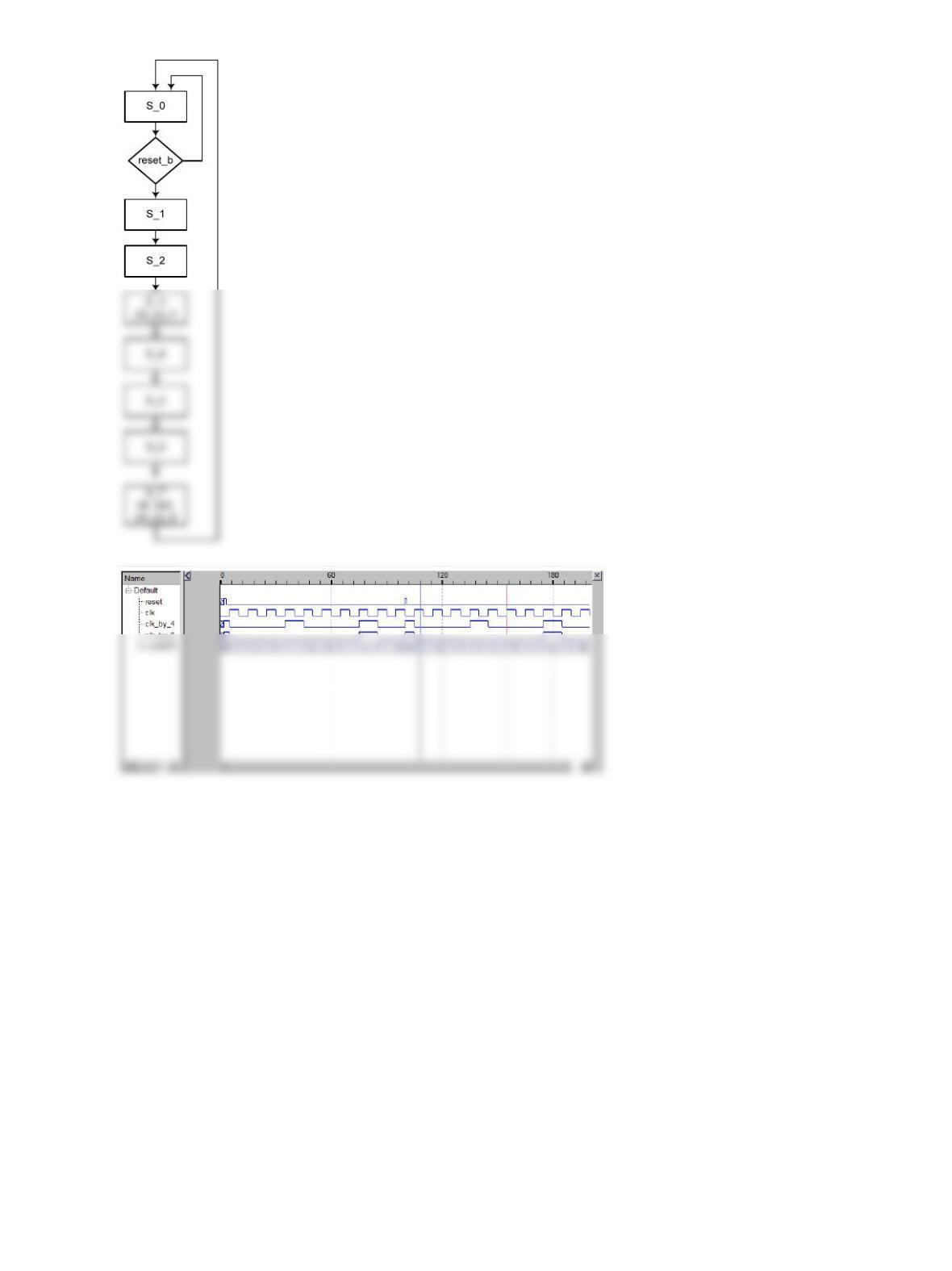
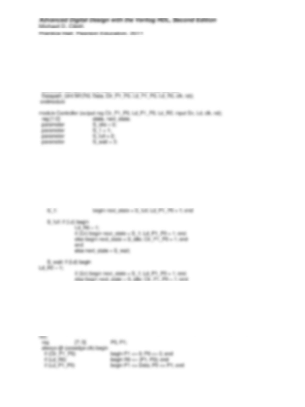
module clk_divider (output clk_by_4, clk_by_8, input clk, reset);
reg [2:0] count;
module t_clk_divider ();
wire clk_by_4, clk_by_8;
reg clk, reset;
clk_divider M0 (clk_by_4, clk_by_8, clk, reset);
Problem 6-19
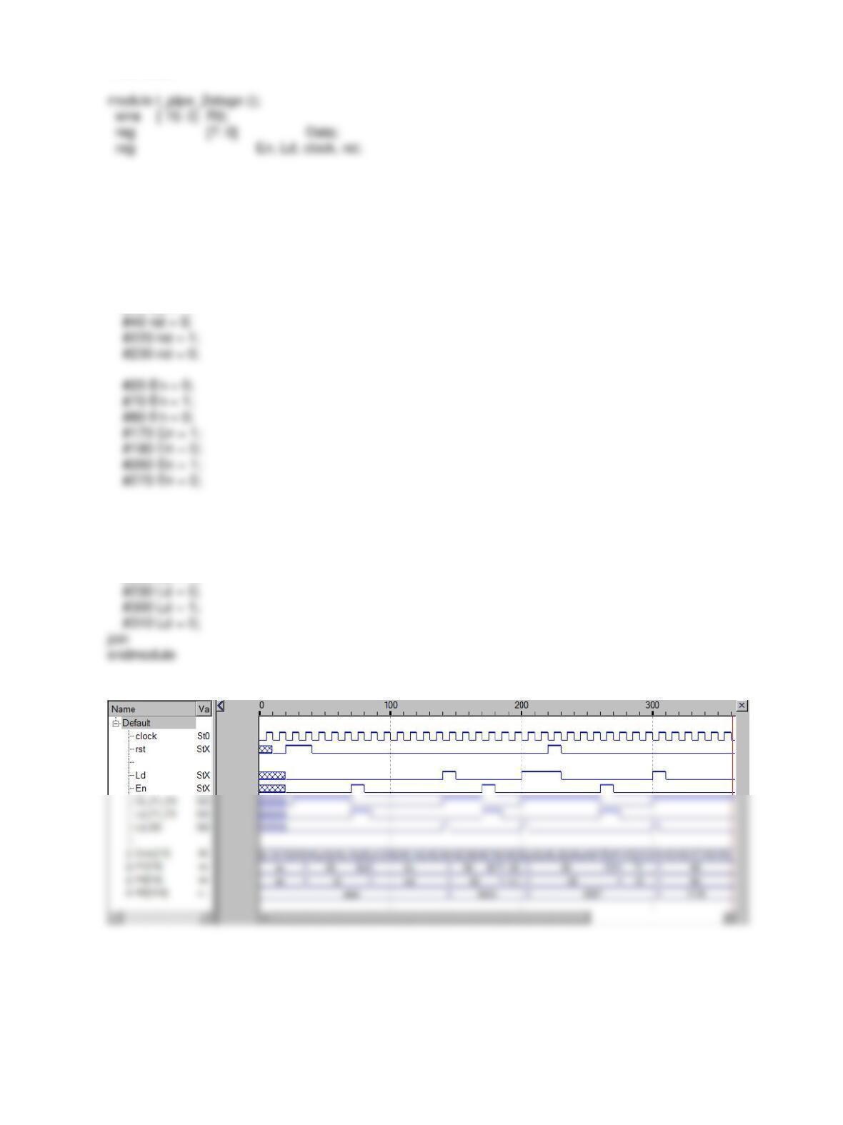
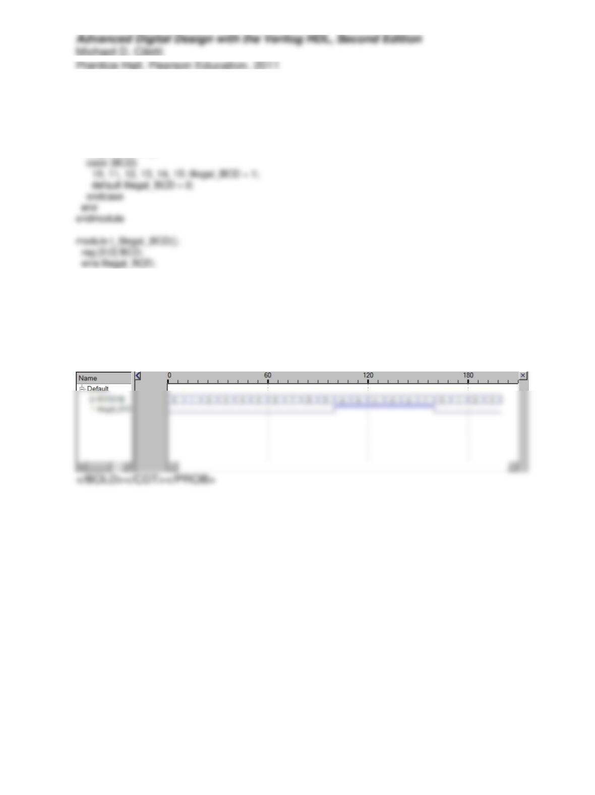
module pipe_2stage (output [15:0] R0, input [7:0] Data, input En, Ld, clk, rst);
wire Clr_P1_P0, Ld_P1_P0, Ld_R0;
Controller M0 (Clr_P1_P0, Ld_P1_P0, Ld_R0, En, Ld, clk, rst);
always @ (posedge clk)
if (rst) state <= S_idle; else state <= next_state;
always @ (state or Ld or En) begin
Ld_P1_P0 = 0; Clr_P1_P0 = 0; Ld_R0 = 0;
case (state)
S_idle: if (rst) begin next_state = S_idle; Clr_P1_P0 = 1; end
else if (En) begin next_state = S_1; Ld_P1_P0 = 1; end
else begin next_state = S_idle; Clr_P1_P0 = 1; end
end
else next_state = S_wait;
default: next_state = 2’bx;
endcase
end
endmodule
module Datapath_Unit (output reg [15:0] R0, input [7:0] Data, input Clr_P1_P0, Ld_P1_P0, Ld_R0, clk,
end
endmodule
pipe_2stage M0 (R0, Data, En, Ld, clock, rst);
initial #500 $finish;
initial begin clock = 0; forever #5 clock = ~clock; end
initial begin Data = 8’H55; forever @ (negedge clock) Data = Data + 1; end
initial fork
#10 rst = 0;
#20 rst = 1;
#20 Ld = 0;
#140 Ld = 1;
#150 Ld = 0;
#200 Ld = 1;
Problem 6-20
module Illegal_BCD (output reg illegal_BCD, input [3:0] BCD);
always @ (BCD) begin
illegal_BCD = 0;
Illegal_BCD M0(illegal_BCD, BCD);
initial #200 $finish;
initial begin
for (BCD = 0; BCD <= 15; BCD=BCD+1)
#10;
end
endmodule
Problem 6-21
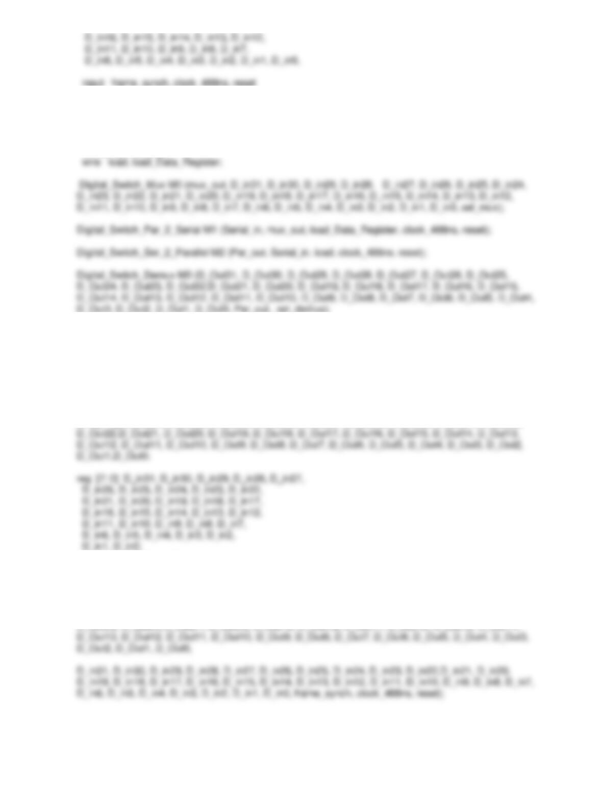
Figure 1 Block diagram for digital switch.
Figure 2 Synchronized frame format.
module Digital_Switch (
output [7: 0] D_Out31, D_Out30, D_Out29, D_Out28, D_Out27, D_Out26, D_Out25, D_Out24,
);
wire [7:0] mux_out;
wire Serial_in;
wire [4: 0] sel_mux;
wire [4: 0] sel_demux;
wire [7:0] Par_out;
Digital_Switch_Control_Unit M4 (sel_mux, sel_demux, load, load_Data_Register, frame_synch,
clock_488ns, reset);
endmodule
`timescale 1 ns / 10 ps
module t_Digital_Switch ();
wire [7: 0] D_Out31, D_Out30, D_Out29, D_Out28, D_Out27, D_Out26, D_Out25, D_Out24, D_Out23,
reg clock_488ns, reset;
reg frame_synch;
parameter clock_488ns_period = 488; // 488 ns
parameter synch_period = 125000; // 125 usec
Digital_Switch M0 (D_Out31, D_Out30, D_Out29, D_Out28, D_Out27, D_Out26, D_Out25, D_Out24,
D_Out23, D_Out22,D_Out21, D_Out20, D_Out19, D_Out18, D_Out17, D_Out16, D_Out15, D_Out14,