Problem 5-1
module Combo_CA (output Y, input A, B, C, D);
assign Y = (~(A | D)) & (B & C & ~D);
endmodule
module t_Combo_CA();
reg A, B, C, D;
wire Y;
#5 {A, B, C, D} = 4’b0100;
#5 {A, B, C, D} = 4’b0101;
#5 {A, B, C, D} = 4’b0110;
#5 {A, B, C, D} = 4’b0111;
#5 {A, B, C, D} = 4’b1000;
#5 {A, B, C, D} = 4’b1001;
Problem 5-2
module Combo_str (output Y, input A, B, C, D);
and (Y, w1, w3);
not (w1, w2);
or (w2, A, D);
and (w3, B, C, w4);
not (w4, D);
endmodule
primitive Combo_prim (output Y, input A, B, C, D);
table
0000 : 0;
0001 : 0;
0010 : 0;
0011 : 0;
0100 : 0;
0101 : 0;
0110 : 1;
0111 : 0;
1000 : 0;
1001 : 0;
1010 : 0;
#5 {A, B, C, D} = 4’b0010;
#5 {A, B, C, D} = 4’b0011;
#5 {A, B, C, D} = 4’b0100;
#5 {A, B, C, D} = 4’b0101;
#5 {A, B, C, D} = 4’b0110;
#5 {A, B, C, D} = 4’b0111;
endmodule
Problem 5-3
module Combo_str_unit (output Y, input A, B, C, D);
and #1 (Y, w1, w3);
not #1 (w1, w2);
or #1 (w2, A, D);
and #1 (w3, B, C, w4);
not #1 (w4, D);
endmodule
0000 : 0;
0001 : 0;
0010 : 0;
0011 : 0;
0100 : 0;
0101 : 0;
0110 : 1;
0111 : 0;
1000 : 0;
1001 : 0;
1010 : 0;
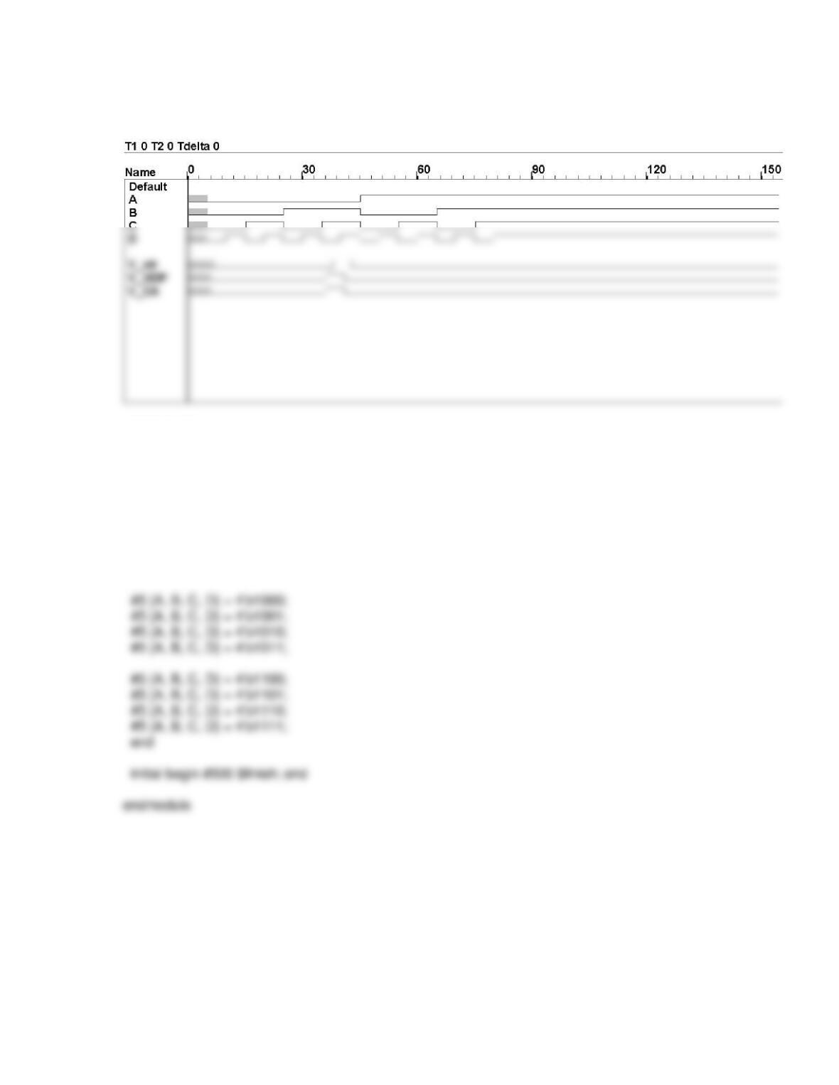
Combo_UDP_unit M1 (Y_UDP, A, B, C, D);
Combo_CA_unit M2 (Y_CA, A, B, C, D);
initial begin
#5 {A, B, C, D} = 4’b0000;
#5 {A, B, C, D} = 4’b0001;
#5 {A, B, C, D} = 4’b0010;
#5 {A, B, C, D} = 4’b0011;
#5 {A, B, C, D} = 4’b0100;
#5 {A, B, C, D} = 4’b0101;
#5 {A, B, C, D} = 4’b0110;
#5 {A, B, C, D} = 4’b0111;
Problem 5-4
module AOI_5_CA1_str (
output y_out,
input x_in1, x_in2, x_in3, x_in4, x_in5, enable
);
and (w1, x_in1, x_in2);
and (w2, x_in3, x_in4, x_in5);
initial begin
#5 enable = 1;
#5 {x_in1, x_in2, x_in3, x_in4, x_in5} = 5’b00000;
#5 {x_in1, x_in2, x_in3, x_in4, x_in5} = 5’b00001;
#5 {x_in1, x_in2, x_in3, x_in4, x_in5} = 5’b00010;
#5 {x_in1, x_in2, x_in3, x_in4, x_in5} = 5’b00011;
#5 {x_in1, x_in2, x_in3, x_in4, x_in5} = 5’b00100;
#5 {x_in1, x_in2, x_in3, x_in4, x_in5} = 5’b00101;
#5 {x_in1, x_in2, x_in3, x_in4, x_in5} = 5’b00110;
#5 {x_in1, x_in2, x_in3, x_in4, x_in5} = 5’b00111;
#5 {x_in1, x_in2, x_in3, x_in4, x_in5} = 5’b10111;
#5 {x_in1, x_in2, x_in3, x_in4, x_in5} = 5’b11000;
#5 {x_in1, x_in2, x_in3, x_in4, x_in5} = 5’b11001;
#5 {x_in1, x_in2, x_in3, x_in4, x_in5} = 5’b11010;
#5 {x_in1, x_in2, x_in3, x_in4, x_in5} = 5’b11011;
#5 {x_in1, x_in2, x_in3, x_in4, x_in5} = 5’b00100;
#5 {x_in1, x_in2, x_in3, x_in4, x_in5} = 5’b00101;
#5 {x_in1, x_in2, x_in3, x_in4, x_in5} = 5’b00110;
#5 {x_in1, x_in2, x_in3, x_in4, x_in5} = 5’b00111;
#5 {x_in1, x_in2, x_in3, x_in4, x_in5} = 5’b01000;
#5 {x_in1, x_in2, x_in3, x_in4, x_in5} = 5’b01001;
#5 {x_in1, x_in2, x_in3, x_in4, x_in5} = 5’b01010;
#5 {x_in1, x_in2, x_in3, x_in4, x_in5} = 5’b01011;
#5 {x_in1, x_in2, x_in3, x_in4, x_in5} = 5’b10100;
#5 {x_in1, x_in2, x_in3, x_in4, x_in5} = 5’b10101;
#5 {x_in1, x_in2, x_in3, x_in4, x_in5} = 5’b10110;
#5 {x_in1, x_in2, x_in3, x_in4, x_in5} = 5’b10111;
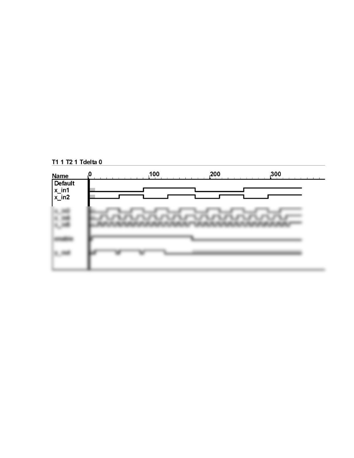
Problem 5-5
module tr_latch (output reg q_out, input enable, data);
always @ (enable, data)
begin
if (enable == 1’b1) q_out = data;
end
initial fork
#100 enable = 0;
#200 enable = 1;
#400 enable = 0;
join
endmodule

Problem 5-6
See the solution to Problem 4-13.
Advanced Digital Design with the Verilog HDL, Second Edition
Michael D. Ciletti
Prentice Hall, Pearson Education, 2011
Problem 5-7
primitive AOI_UDP (
output y,
input x_in1, x_in2, x_in3, x_in4, x_in5
);
table
// x1 x2 x3 x4 x5
0 0 0 0 0 : 1;
0 0 0 0 1 : 1;
0 0 0 1 0 : 1;
1 0 0 0 0 : 1;
1 0 0 0 1 : 1;
1 0 0 1 0 : 1;
1 0 0 1 1 : 1;
1 0 1 0 0 : 1;
1 0 1 0 1 : 1;
1 0 1 1 0 : 1;
1 0 1 1 1 : 0;
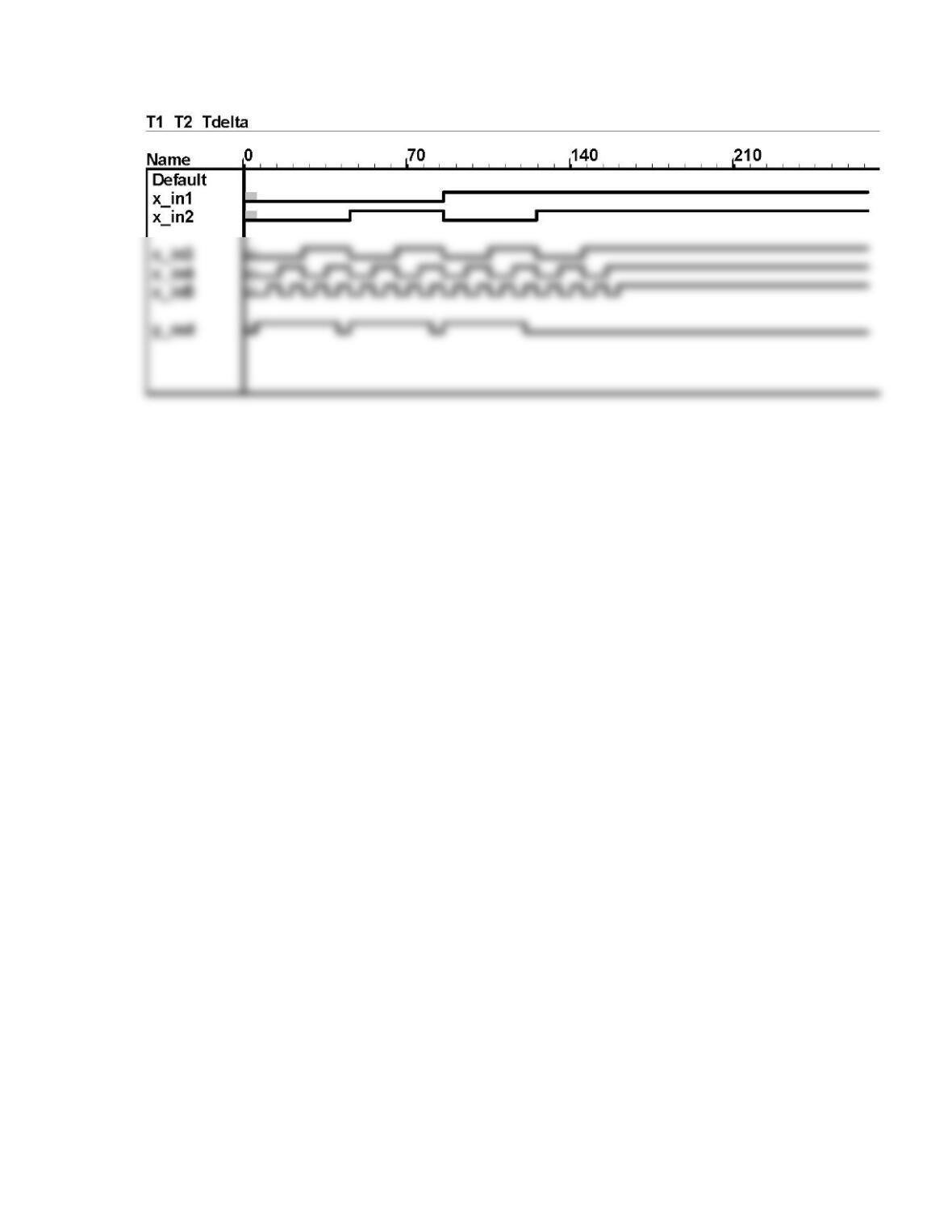
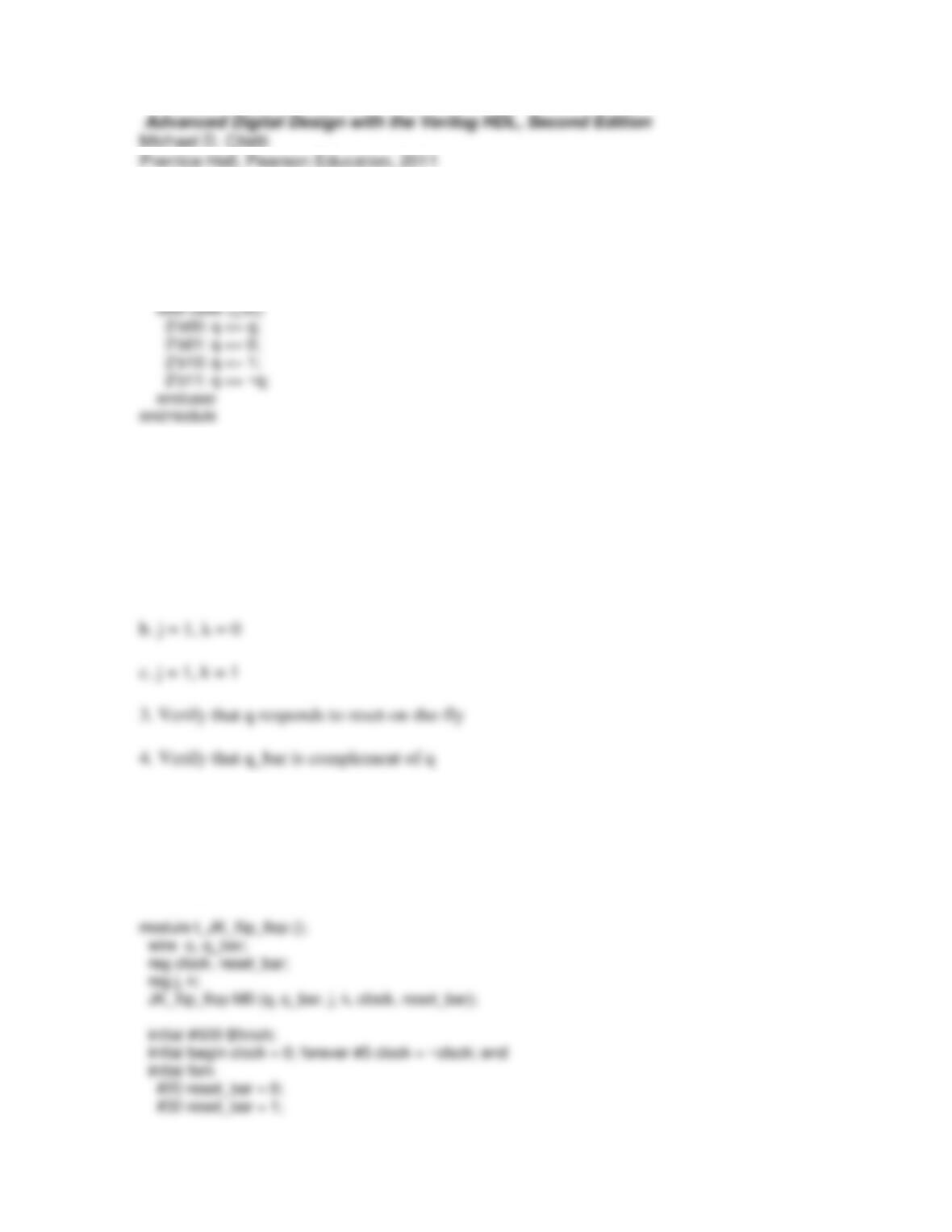
module t_AOI_UDP_mod();
reg x_in1, x_in2, x_in3, x_in4, x_in5;
wire y_out;
AOI_UDP_mod M0 (y_out, x_in1, x_in2, x_in3, x_in4, x_in5);
initial #350 $finish;
#5 {x_in1, x_in2, x_in3, x_in4, x_in5} = 5’b01001;
#5 {x_in1, x_in2, x_in3, x_in4, x_in5} = 5’b01010;
#5 {x_in1, x_in2, x_in3, x_in4, x_in5} = 5’b01011;
#5 {x_in1, x_in2, x_in3, x_in4, x_in5} = 5’b01100;
#5 {x_in1, x_in2, x_in3, x_in4, x_in5} = 5’b01101;
#5 {x_in1, x_in2, x_in3, x_in4, x_in5} = 5’b11000;
#5 {x_in1, x_in2, x_in3, x_in4, x_in5} = 5’b11001;
#5 {x_in1, x_in2, x_in3, x_in4, x_in5} = 5’b11010;
#5 {x_in1, x_in2, x_in3, x_in4, x_in5} = 5’b11011;
#5 {x_in1, x_in2, x_in3, x_in4, x_in5} = 5’b11100;
Problem 5-8
module JK_flip_flop (output reg q, output q_bar, input j, k, clock, reset_bar);
assign q_bar = ~q;
always @( posedge clock, negedge reset_bar)
if (reset_bar == 0) q <= 0;
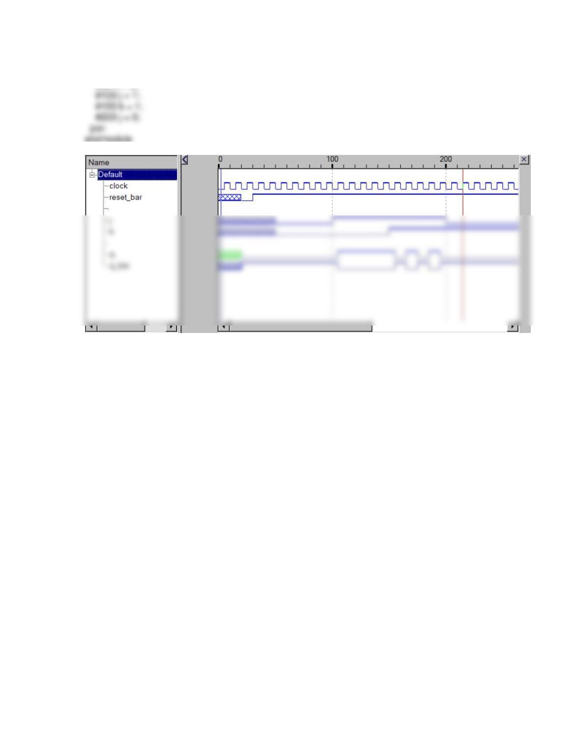
Test plan:
1. Verify that q responds to initial reset
2. Verify that q responds to j = 0, k = 0
a. j = 0, k = 1
5. Verify that reset action is active low and asynchronous
6. Verify that transitions between clock edges are ignored
7. Verify that reset_bar overrides the clock
#50 j = 0;
#50 k = 0;
endmodule
Problem 5-9
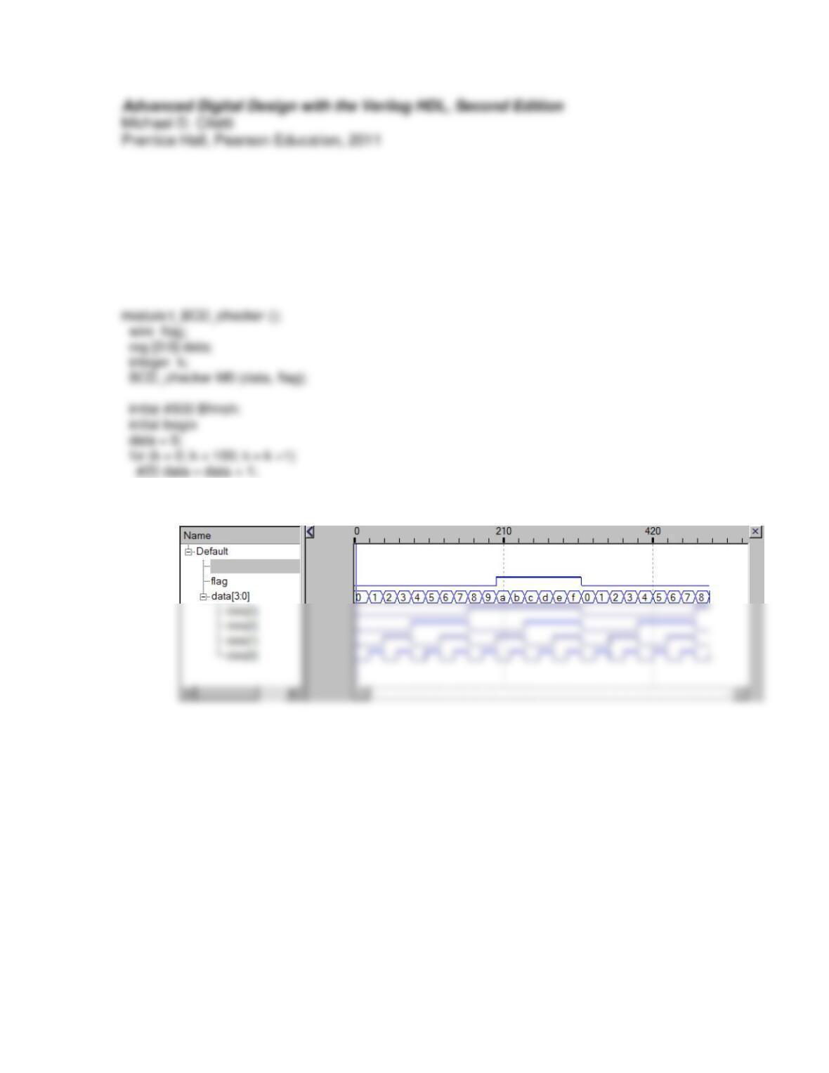
module BCD_checker (input [3:0] data, output reg flag);
always @ (data)
case (data)
0, 1, 2, 3, 4, 5, 6, 7, 8, 9: flag = 0;
default: flag = 1;
endcase
endmodule
end
endmodule
Problem 5-10
The for loop executes if K <= 15. If K is declared as a 4-bit register it will roll over from
Michael D. Ciletti
Prentice Hall, Pearson Education, 2011
Problem 5-11
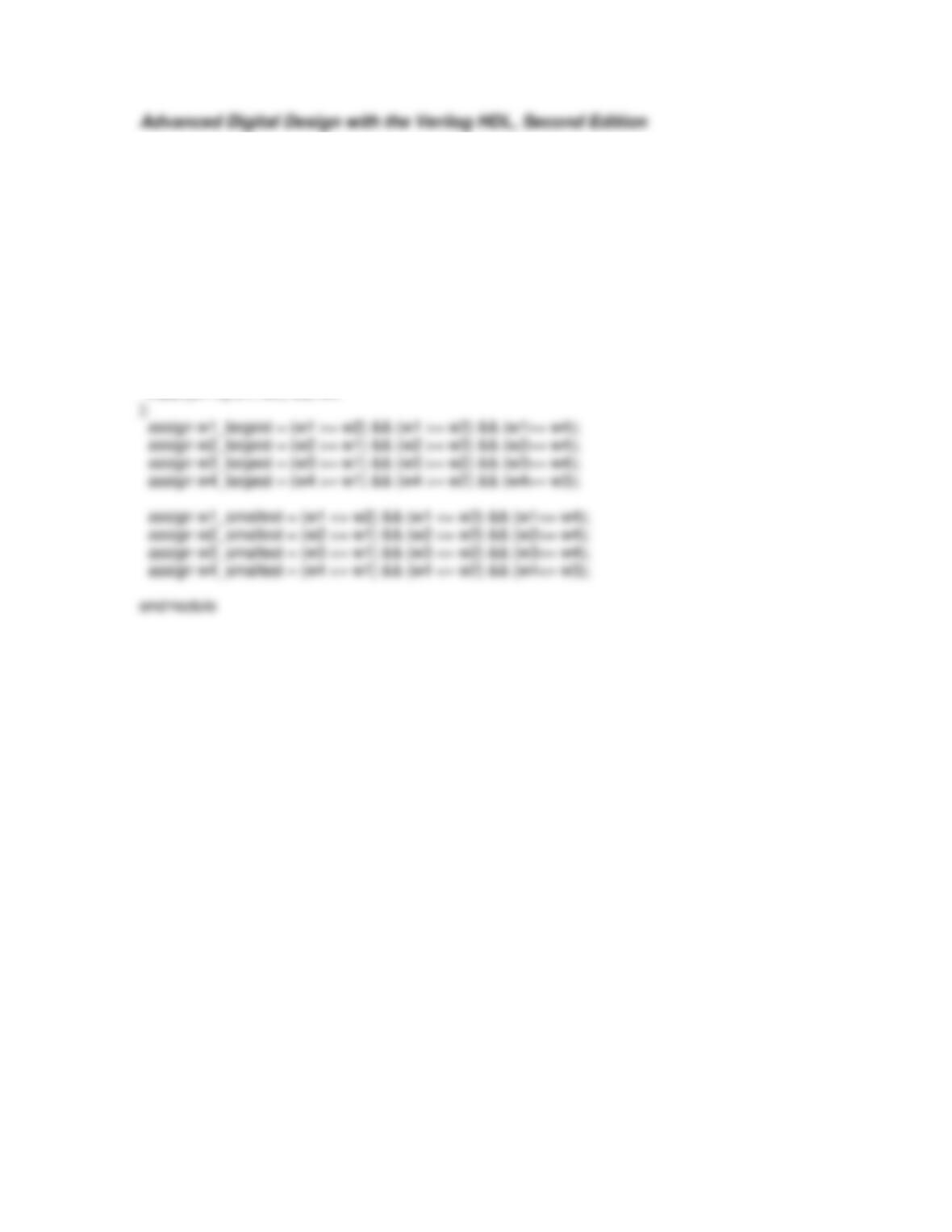
module Prob_5_11 (
output w1_largest, w2_largest, w3_largest, w4_largest,
output w1_smallest, w2_smallest, w3_smallest, w4_smallest,
input [31: 0] w1, w2, w3, w4
Problem 5-12
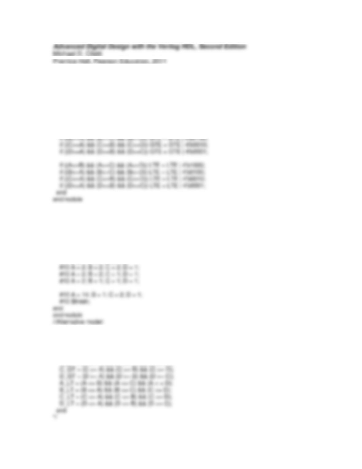
module Prob_5_12 (output reg [3: 0] GTE, LTE, input [31: 0] A, B, C, D);
always @ (A, B, C, D)
begin
GTE = 0;
LTE = 0;
if ((A>=B) && (A>=C) && (A>=D)) GTE = GTE | 4’b1000;
module t_Prob_5_12 ();
wire [3:0] GTE, LTE;
reg [31: 0] A, B, C, D;
Prob_5_12 M0 (GTE, LTE, A, B, C, D);
initial begin
A = 2; B = 2; C = 2; D = 2;
/*
always @ (A, B, C, D)
begin
A_GT = (A >= B) && (A >= C) && (A > = D);
B_GT = (B >= A) && (B >= C) && (C >= D);