Unlock document.
This document is partially blurred.
Unlock all pages and 1 million more documents.
Get Access
229
Unit 18 Solutions
Unit 18 Problem Solutions
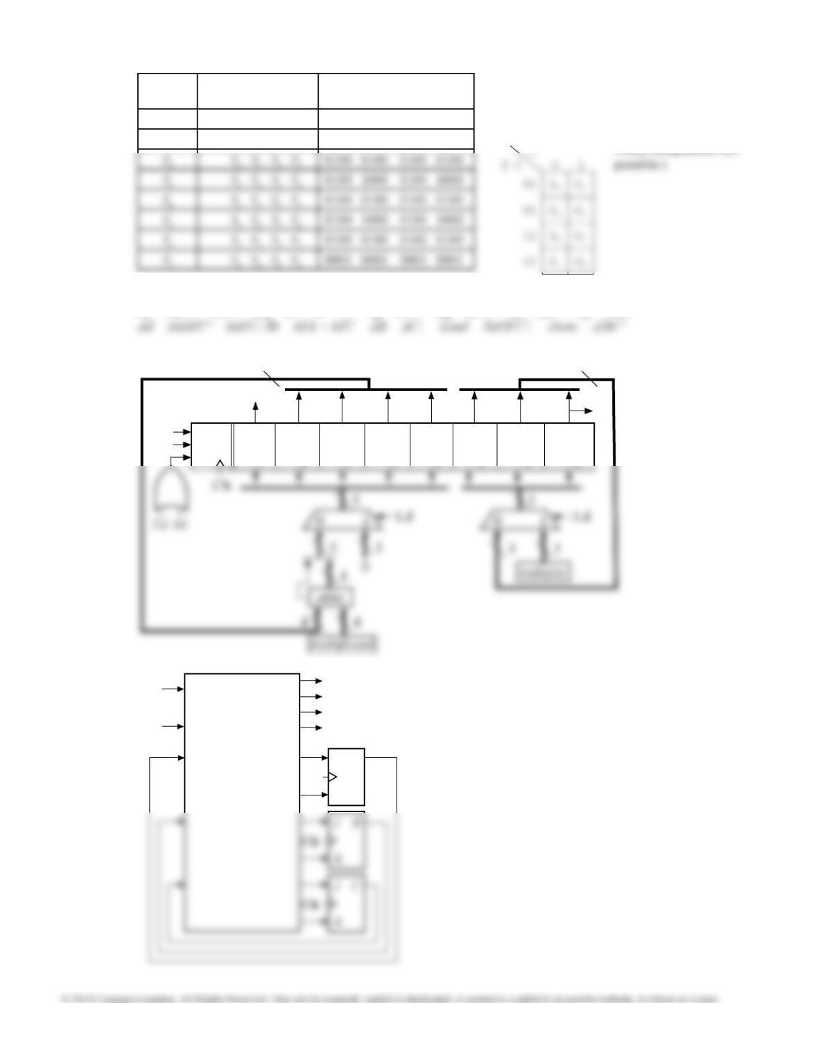
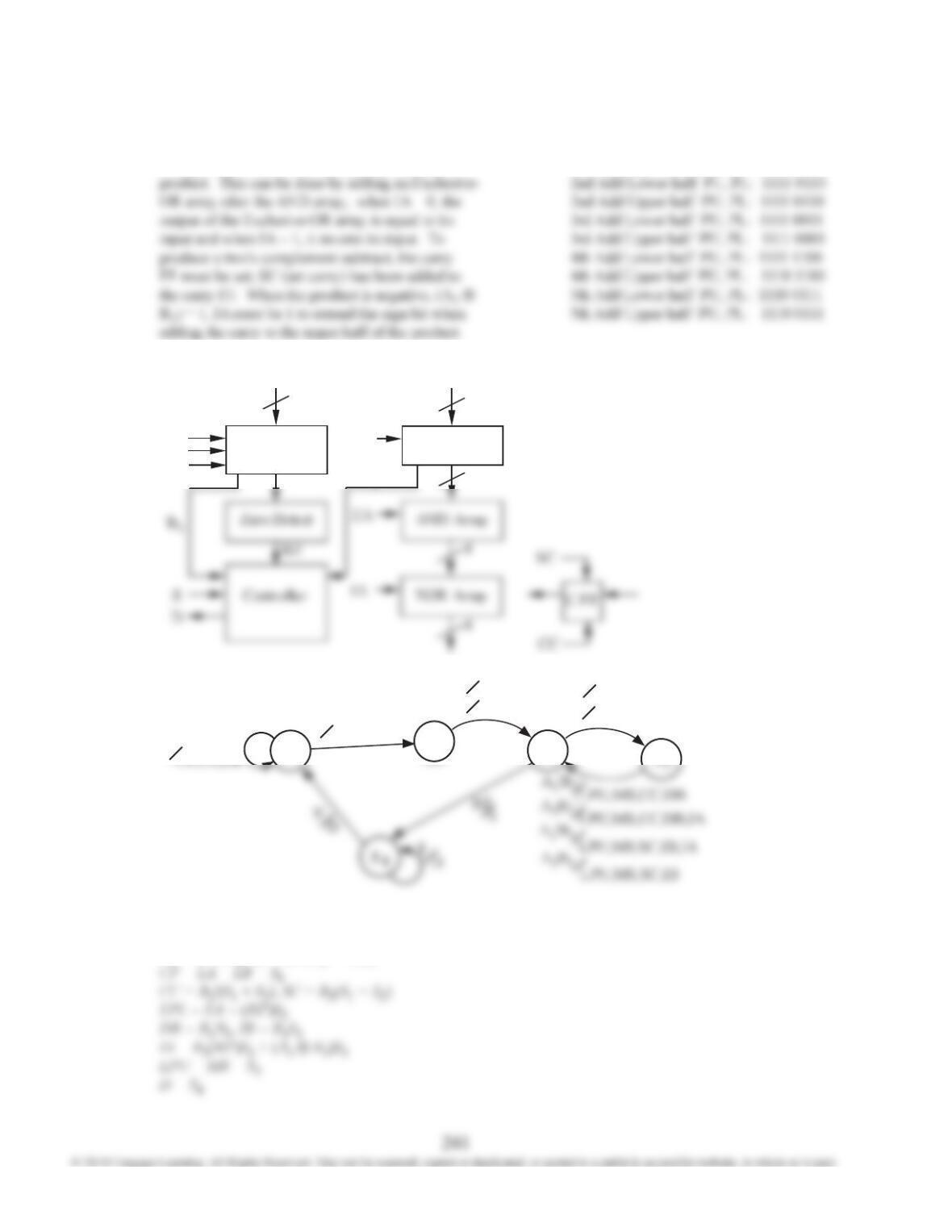
18.3 See FLD p. 775 for circuit. Notice that the Q
output of the ip-op is bin
, while the D input is bout
.
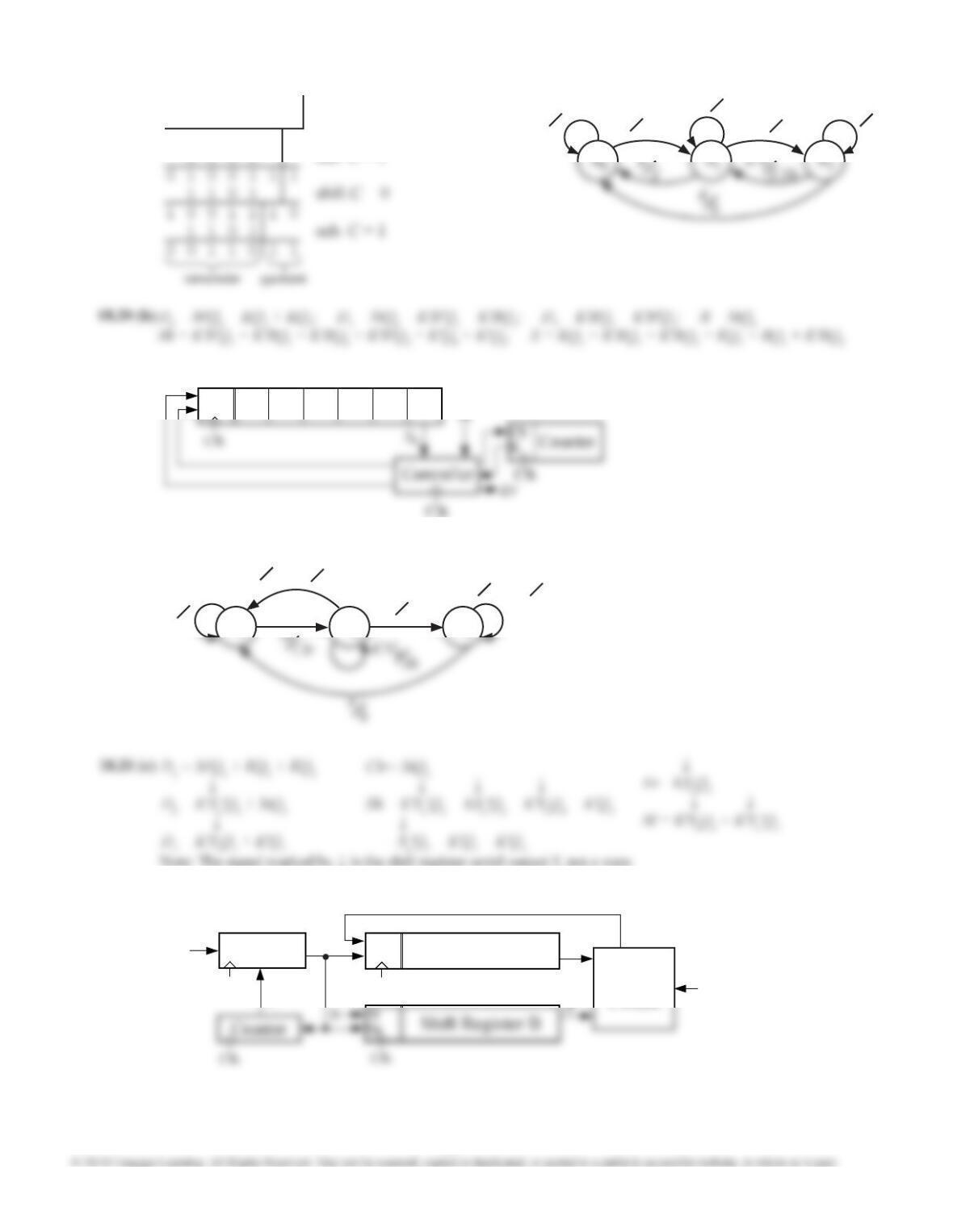
18.4
S0
St'0
See FLD p. 775. AND-ing with xi is like M/Ad if
xi is 1. Shifting is like moving from AND gates
involving x1 to those involving x2, or from x2 to x3.
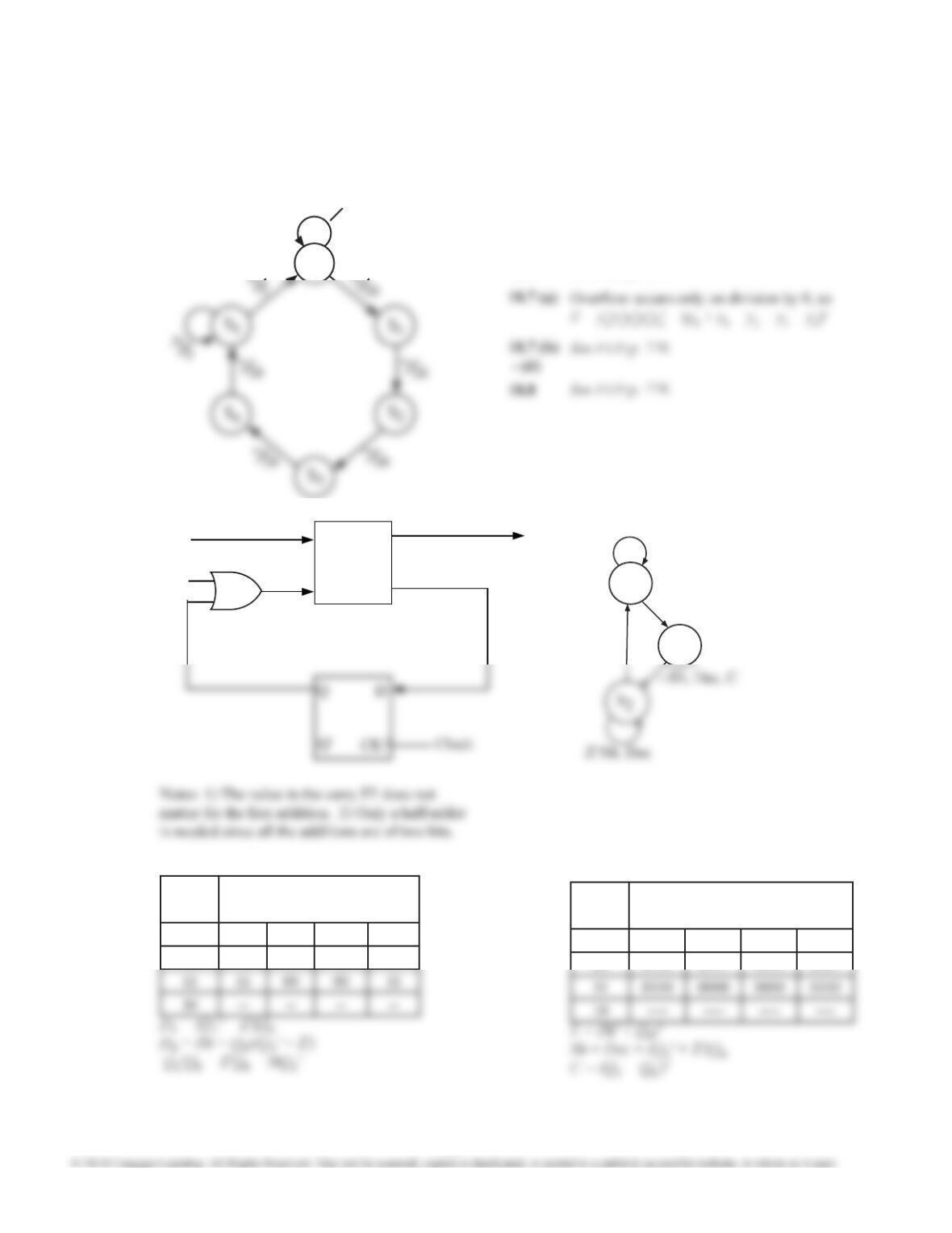
18.5 See FLD p. 776. Compare to divider state graph of
FLD Figure 18-11.
18.6 See FLD p. 776.
18.9
DA
Co
S
X
B
HA
C
CC
S1
St'/-
St/L
Z/-
S0
Next State Table: S0 = 00, S1 = 01, S2 = 11
St Z
Q1Q000 01 11 10
00 00 00 01 01
01 11 11 11 11
Output Table: L Sh Dec C
St Z
Q1Q000 01 11 10
00 0000 0000 1000 1000
01 0111 0111 0111 0111
230
Unit 18 Solutions
18.10
DA
Co
S
X
B
HA
C
CC
St'/-
St/L
Z/-
S3
S0
Z'/Sh, Dec
Next State Table: S0 = 00, S1 = 01, S2 = 11, S3 =
10
St Z
Q1Q000 01 11 10
00 00 00 01 01
Output Table: L Sh Dec C
St Z
Q1Q000 01 11 10
00 0000 0000 1000 1000
18.11
DA
Co
Ci
S
X
BFA
C
CC
St'/-
St/L
Z/-
S0
231
Unit 18 Solutions
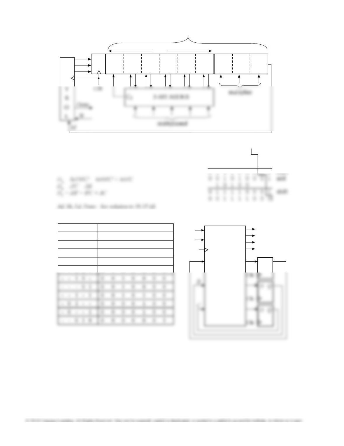
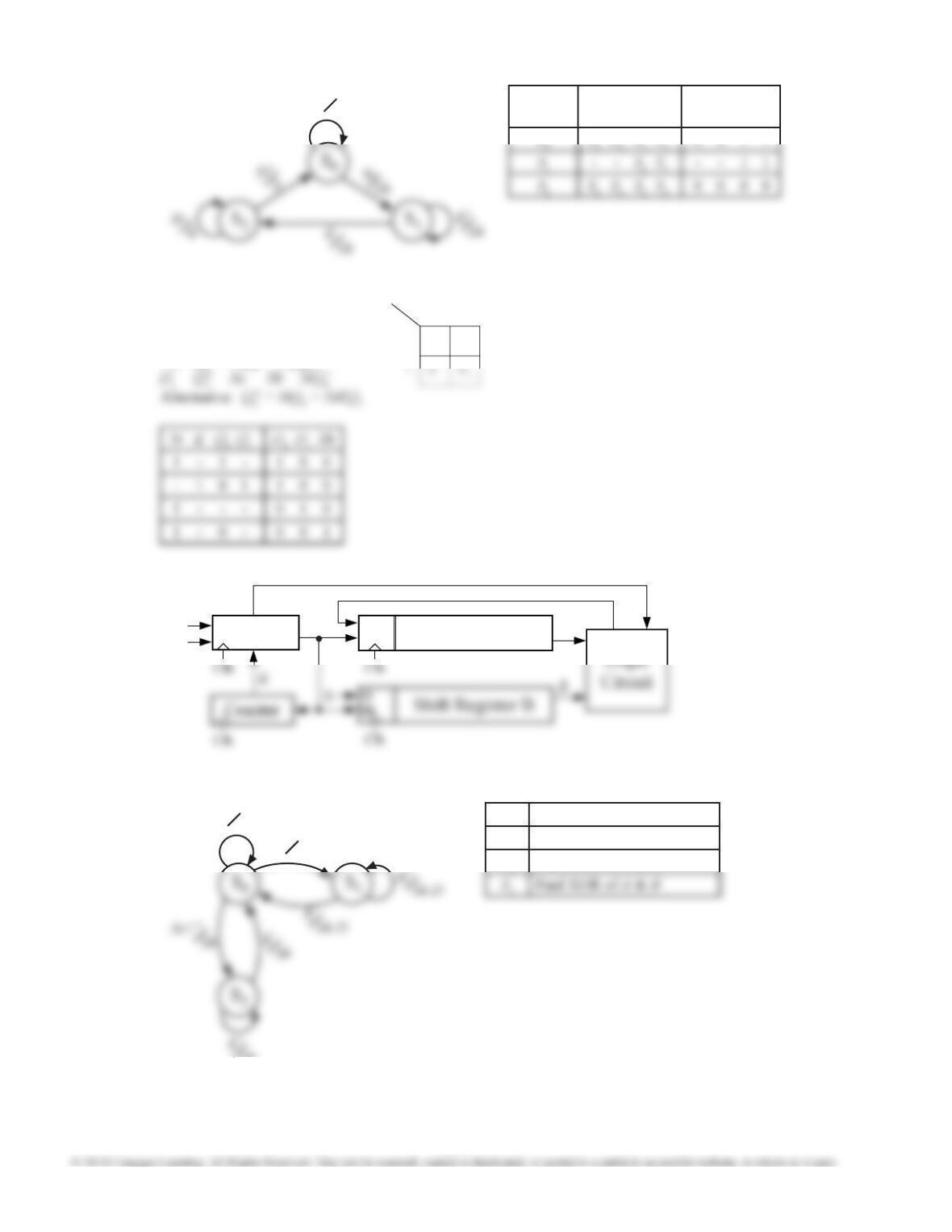
18.12 (a) Inputs and outputs are given in decimal in the table. Inputs 10 through 14 are assumed to never occur.
0 1 2 3 4 5 6 7 8 9 15
18.13 (a) Inputs and outputs are given in decimal in the table. Inputs 1, 2, 13, 14, and 15 are assumed to never occur.
0 3 4 5 6 7 8 9 10 11 12
A A, 0 A, 3 B, 12 B, 11 B, 10 B, 9 B, 8 B, 7 B, 6 B, 5 B, 4
Use the state assignment Q = 0 for state A and Q = 1 for state B. There are 159 minimum sum-of-product equations
for Q+; one solution is
Q+ = X3'X0 + X3'X2 + X3'X1 + X3X2' + QX2'.
18.12 (b)
Use the state assignment Q = 0 for state A and Q = 1 for state B. The minimum sum-of-product equations for Q+ and
the outputs are
Q+ = X3 + X2 + QX0 or
18.13 (b)
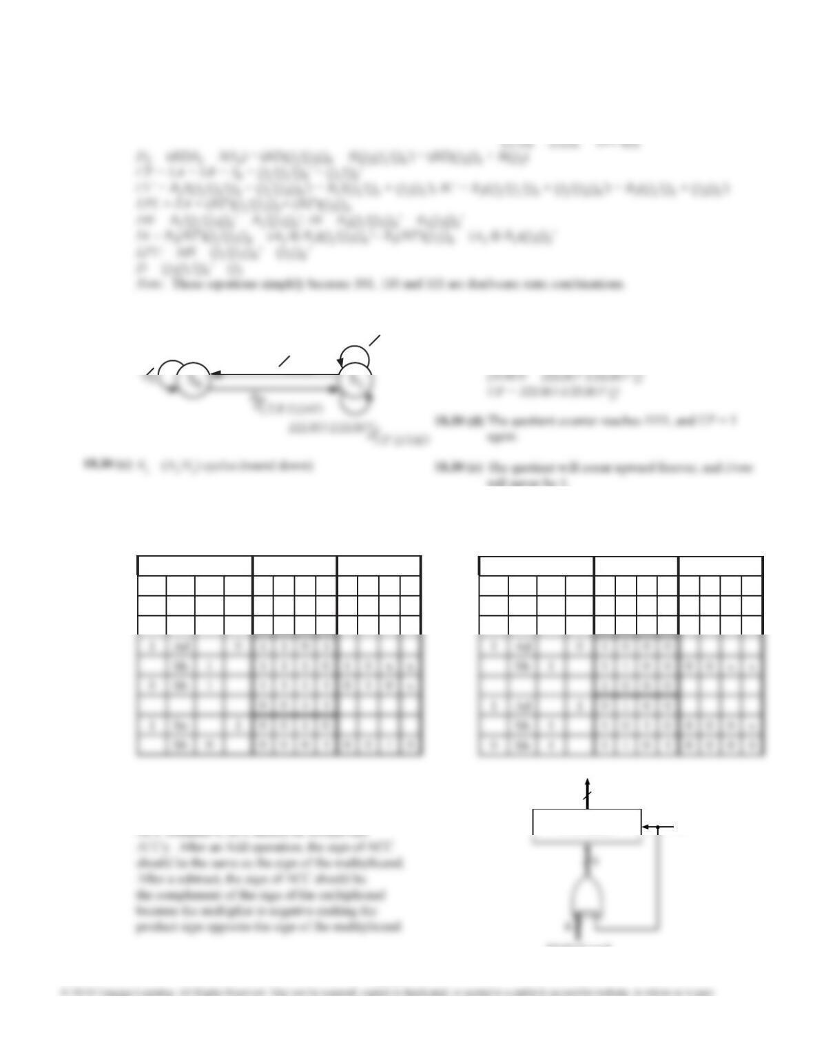
18.14 The ONE ADDER is similar to a serial adder,
except that there is only one input. This means that
the carry will be added to X. Thus, if the carry ip-
op is initially set to 1, 1 will be added to the input.
The signal I can be used to preset the carry ip-op
to 1.
Q
X Sh 0 1
00
01
11
0
0
0
1
0
1
Q
X Sh 0 1
00
01
11
0
0
1
0
1
0
232
Unit 18 Solutions
18.15 (a)
18.15 (b) 18.15 (c)
S1
S9
S0
St/Load
M/Ad
- /Done
St'/0
S
- /Sh
7
3456 0127
ACC
product
C
Sh
Load
1 0 1 1
0 0 0 0 0 1 0 1
0 1 0 1 1 1 0 1
0 0 0 1 0 1 1 1
1 0 1 1
0 0 1 0 1 1 1 0
0 1 1 0 1 1 1 1
add
shift
shift
add
shift
IQ
X
Q'
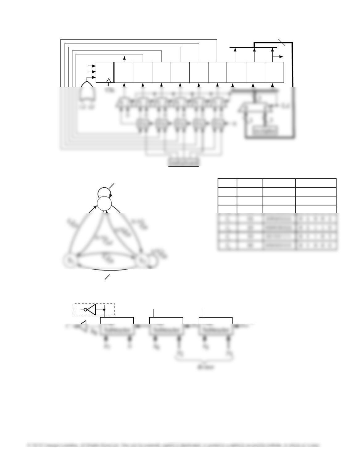
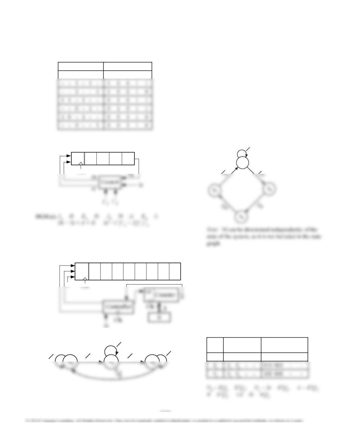
18.14
(cont.)
233
Unit 18 Solutions
Present
State
Next State
StM: 00 01 10 11
Ad Sh Load Done
00 01 10 11
S0 S0 S0 S1 S1 0000 0000 0010 0010
S1 S3 S2 S3 S2 0100 1000 0100 1000
18.15 (d)
(Other assignments are
I. (S0, S7) (S1, S2) (S3, S4) (S5, S6)
II. (S0, S1) (S2, S3) (S4, S5) (S6, S7)
III. (S1, S3, S5) (S2, S4, S6) etc.
For this assignment, from LogicAid:
JA = StB'C' + MC; KA = M' + B + C; JB = A'C; KB = A'C'; JC = AB'; KC = A'B;
Sh
Ld
SI
Q7Q6Q5Q4Q3Q2Q1Q0
D7D6D5D4D3D2D1D0
M
34
0
Sh
A
K
J
Clk
St
M
Ad
Sh
Ld
Done
OR gates, AND
gates, & inverters
implement the
equations from
18.15 (d)
234
Unit 18 Solutions
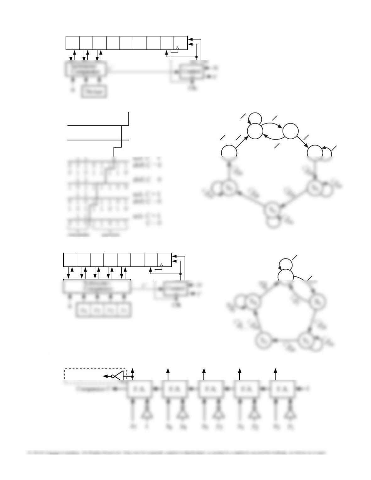
18.16 (a)
4567 0128
ACC
product
C
O
N
Sh
Ad
Load
3
St M A B C DA DB DC Ad Sh Ld Done
1 - 0 0 0 1 0 0 0 0 1 0
- 1 1 0 0 1 0 0 1 0 0 0
- 1 0 - 1 1 0 0 1 0 0 0
- - 0 - 1 0 1 0 0 0 0 0
- - 1 1 - 0 1 0 0 1 0 0
Q
D
St
M
Ad
Sh
Ld
Done
PLA
Clk
A
Graph is same as 18.15, so from LogicAid, using
the same state assignment:
18.16 (d)
18.16 (c)
0 0 0 0 0 0 0 1 1
0 0 0 0 0 0 1 1 0
1 0 1 0 0
shift
add
18.16 (b) See solution to 18.15 (b).
235
Unit 18 Solutions
Sh
Ld
SI
Q7Q6Q5Q4Q3Q2Q1Q0
D7D6D5D4D3D2D1D0
M
3
0
Sh
Q8
D8
18.16 (d)
(cont.)
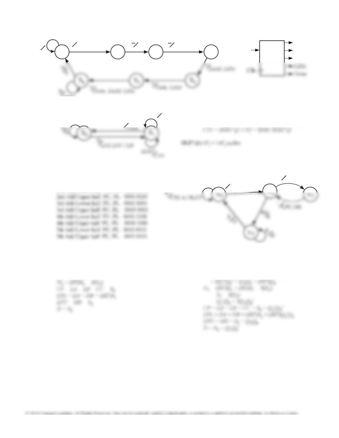
18.17 (a)
S
0
St'0
MAd
State Counter X St M K Ad Sh
S000 000000111 1 1 0 1 0
S100 011001111 0 1 0 0 1
S201 001100111 0 1 0 1 0
18.17 (b)
18.18 (a)
d7
b7Full
d6
b6Full
d5
b5
C
(alternate solution)
236
Unit 18 Solutions
Sh
Ld
x0
x1
x2
x3
x4
x5
x6
x7
18.18 (b)
18.18 (d)
1 1
0 1 0 1 0 0 1 1
1 0 1 0 0 1 1 0
0 1 0 0 0 1 1 1
1 0 0 0 1 1 1 0
1 1
shift C = 0
sub. C = 1
shift C = 0
S2
S6
S0
St
Ld
C'0CSu
St'0
S1
C'Sh
CV
CSu ,
18.18 (c)
18.19 (c)
d7
d6
d5
d4
d3
Comparator C
alternate solution
Sh
Ld
x1
x2
x3
x4
x5
x6
x7
ShSu
S0
St Ld
St'0
18.19 (a) 18.19 (b)
237
Unit 18 Solutions
18.19 (d) 18.20 (a)
SI
Sh
18.21 (a)
1 1 0 1
1 0 1 1 0 1 0
shift C = 0
sub. C = 1
1 1 0 1
0 1 0 1 1 0 1
St'
0
K'B'
Sh
St
R
K'B'
Sh
K'B
X Sh
18.22 (a)
Control
St
Clk
Clk
SI
Sh
Logic
Circuit
a
Shift Register A
C
Sh
K
SI
Clk
S2S3
S1
St'
0
K'
Sh
K'
Sh SI
K
Sh
K' Sh SI
K
Er
,
,
S'
oSo
So
SoS'
o
18.21 (b)
Note: The signal marked by ↓ is the shift register serial output So not a state.
238
Unit 18 Solutions
18.22 (b)
St'
0
Present
State
StK
00 01 11 10
Sh
00 01 11 10
18.22 (c) I. (S0, S2)×2 (S1, S2) (S0, S1)
II. (S0, S2)×2 (S1, S2) (S0, S1)×2
From Karnaugh maps:
D0 = Q0
+ = StQ0 + KQ0
'Q1
18.22 (d) SI = C'ab + Cab' + Ca'b
S0
0 1
0
18.23 (a)
Control
St
SI
Sh
a
Shift Register A
CSh
SI
D
St'
0
St C
Sh D
Sh
18.23 (b) State Meaning
S0Reset
S1Find AND of A & B
239
Unit 18 Solutions
St C K Q0 Q1 Q2 Q1
+ Q2
+ Q3
+ Sh D
0 - - 1 - - 1 0 0 0 0
18.24 (a)
Sh
X
SI
Clk
18.24 (b)
S0
St'0
St Sh
-Sh
A
B
SI
18.25 (a)
Q0
+ = St'Q0 + KQ1 + KQ2; Q1
+ = StCQ0 + K'Q1;
Q2
+ = StC'Q0 + K'Q2;
Sh = StCQ0 + StC'Q0 + K'Q1 + KQ1 + K'Q2 + KQ2
D = StCQ0 + K'Q1 + KQ1
18.23 (c) Change C' to D' in 18.22 (d)
SI = D'ab + Dab' + Da'b
18.23 (d)
St'
0
K
Ld
K'
A
K'B
St
Ld
18.25 (b)
State
StK
00 01 11 10
ABLd
00 01 11 10
S0 S0 S0 S1 S1 000 000 001 001
18.25 (c)
240
Unit 18 Solutions
J = ST; K = ZER1 ZER2;
Done = ZER1 ZER2 Q; CLR = STQ';
LD2 = STQ'; LD1 = STQ' + ZER1 ZER2' Q;
18.27 (a) 18.27 (b)
ZER1 ZER2
ZER1 ZER2'
CT2 LD1
18.26
Control
St LdAd
EnIn
EnAd
St'
0
St
LdAc, EnIn
S0S1S2S3
0
EnIn, LdAd
Done
Initial PU,PL: 0000 0000
1st Add Lower half PU, PL: 0000 1011
1st Add Upper half PU, PL: 0000 1011
2nd Add Lower half PU, PL: 0000 0110
18.28 (a)
SCP,LA,LB,CC
BZ'
LPL,EA,DB
18.28 (b)
Label the 4 FF outputs S0, S1, S2 and S3.
D0 = S'S0 + S'S3
D1 = S(S0) + S2
D2 = (BZ')S1
18.28 (c) Assume two FFs Q1Q0 and the following encoding:
S0 = 00, S1 = 01, S2 = 11, and S3 = 10. Then,
D0 = S(S0) + S2+ (BZ')S1
= SQ1'Q0' + Q1Q0 + (BZ')Q1'Q0
18.28 (d)
Unit 18 Solutions
Answer is the same for both parts of Part (b).
Initial PU,PL: 0000 0000
1st Add Lower half PU, PL: 0000 1011
1st Add Upper half PU, PL: 1111 1011
18.29 (b)
S0
S2
S1
S' CP,LA,LB
SCP,LA,LB
B3'CC
S3
B3'BZ'LPL,EA
B3SC B3BZ' LPL,EA,IA
18.29 (c)
18.29 (a)
B Counter
4
Multiplier
LB
DB
A Reg
4
LA
Multiplicand
4
to adder
IB
A3
When the multiplier is negative, the B counter can
be incremented to zero. Two control inputs are
assumed: DB (decrement B) and IB (Increment
B). Also, when the multiplier is negative, the
multiplicand must be subtracted to produce the
Label the 5 FF outputs S0, S1, S2, S3 and S4.
D0 = S'S0 + S'S4, D1 = S(S0), D2 = S1 + S3
D3 = (BZ')S2, D4 = (BZ)S2 + S(S4)
18.29 (d)
Note: The PU and PL registers are connected the
same way as in Problem 18.28.
242
Unit 18 Solutions
18.30 (a)
St'
EZERO
Done
IZERO' EZERO'
DOWN
D = EZERO' Q + StQ'; Done = EZERO Q;
CLR = StQ';
LOAD = StQ' + IZERO EZERO' Q
18.30 (b)
will never be 1.
Assume three FFs Q2Q1Q0 and the following encoding: S0 = 000, S1 = 001, S2 = 011, S3 = 010 and S4 = 100. Then,
D0 = S(S0) + S1+ S3 = SQ2'Q1'Q0' + Q2'Q1'Q0 + Q2'Q1Q0' = SQ1' + Q1'Q0 + Q1Q0' or
= SQ0' + Q1'Q0 + Q1Q0'
D1 = S1 + S3 + (BZ')S2 = Q2'Q1'Q0 + Q2'Q1Q0' + (BZ')Q2'Q1Q0 = Q1'Q0 + Q1Q0' + (BZ')Q1 or
18.29 (e)
A = 11012 = -310, B = 10102 = 610
B X A = 0001 00102 = 1810
PU PL
biOp Sin C40000xxxx
0 Sh 0 – 00000xxx
1101
18.31 (a) A = 10002 = -810, B = 01102 = 610
B X A = 1101 00002 = -4810
PU PL
biOp Sin C40000xxxx
0 Sh 0 – 0 0 0 0 0 x x x
1000
Since the number in ACC is a two’s complement
number, the sign of this number should be shifted
into ACC7. Before any add or subtract operations
18.31 (b) 18.31 (c)
18.31 (b)
4
4-bit adder Su
Multiplicand
243
Unit 18 Solutions
18.31 (c)
cont.
Clk
Q
Q'
J
K
M3
Ad
Su 7
to ACC
Ad
M ′
3
S1
S9
S8
S0
St/Load
–/Done
St'/0
–/Sh
M'/Sh
18.31 (d)
S0 S1
K'M'/Sh
S t'/0
St/Load
18.31 (e) 18.32 (a) 1 0111 0 0111
- (0) 1101 - (0) 1101
0 1010 1 1010
1 1011 0 1011
- (0) 1001 - (0) 1001
18.32 (b) The following case cannot occur:
1 101
- (0) 1001
18.32 (c) Subtraction should be done if X8 = 1 or if X8 = 0
and b8 = 0, so C = X8 + b8'.
S
0
S
1
S
2
S
C′/Sh
C′/Sh
C/Su
C/V
St/Load
18.33 (a)
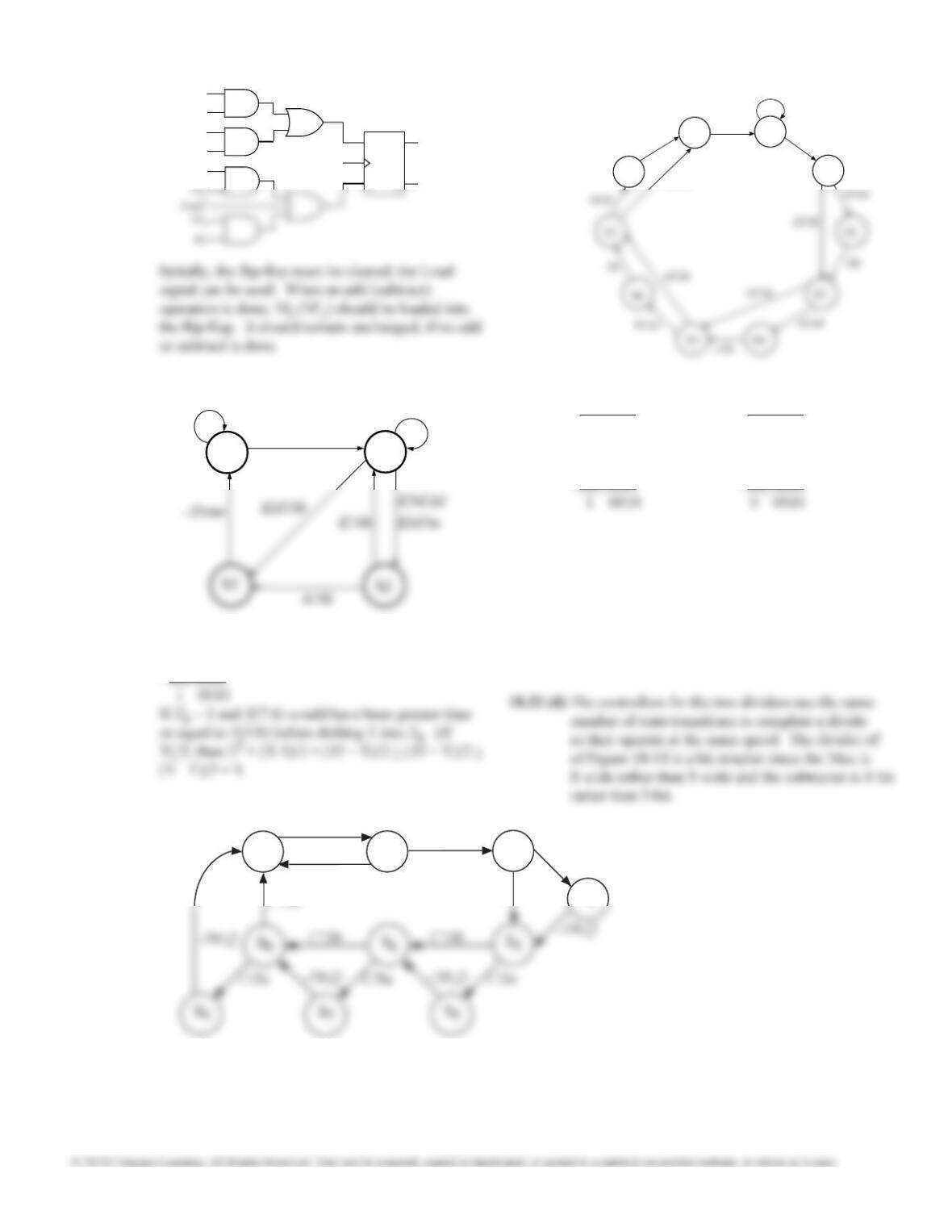
18.32 (d) The controllers for the two dividers use the same number of state transitions to complete a divide so they operate
at the same speed. The divider of of Figure 18-15 is simpler since the Mux is 4-wide rather than 9-wide and the
subtracter is 4-bit rather than 5-bit. However, the controller requires more states so it will be more complex.
244
Unit 18 Solutions
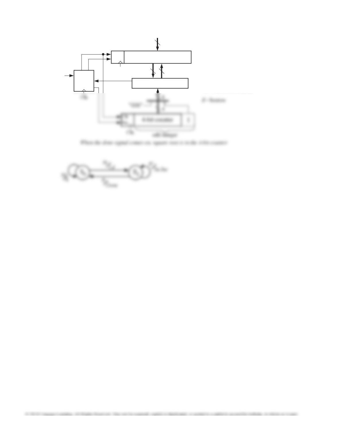
18.34
Clk
Ld
8-bit subtracter
Control
Circuit
N
B
8-bit register
Su
8
8
8
SuLd
St
St - start
Ld - load N into register
and clear counter
Su - load subtracter output
into register
Inc - increment counter


