Problem Solutions – Chapter 8
1
CHAPTER 8
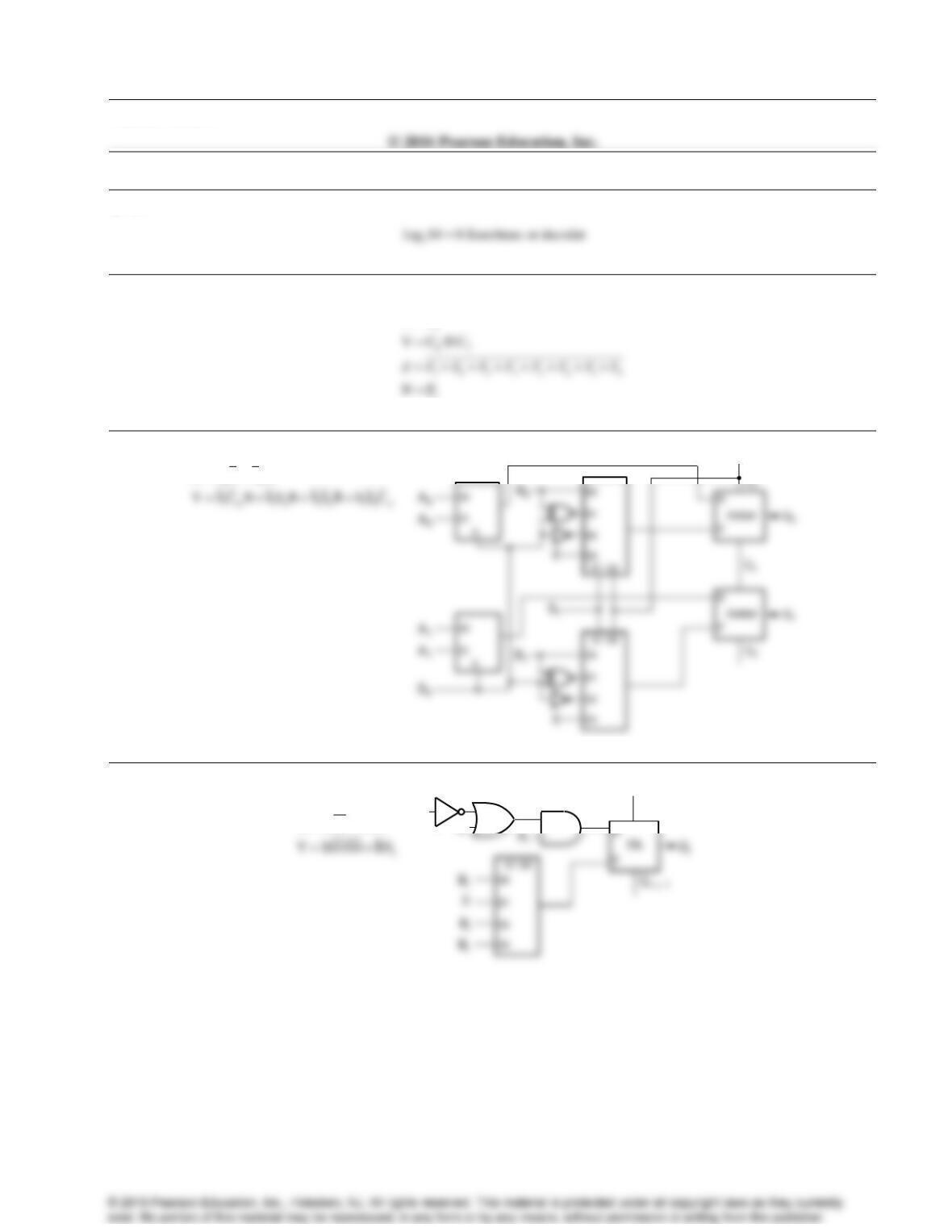
8-1.
8-2.*
8
CC
8-3.*
00
X S A S A
X = S0A + S0A
Cin
8-4.*
X AS1 AS0
Ci
X = A S1 + A S0
S1
S0
Problem Solutions – Chapter 8
2
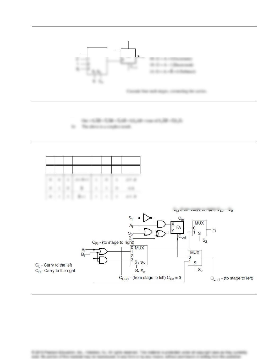
8-5.
Connect to Cin for first stage.
Ci
X
Connect to Cin for first stage.
Ai
MUX
0
Bi
00: G = A + B (Add)
Ci
X
Connect to Cin for first stage.
Ai
MUX
0
Bi
00: G = A + B (Add)
00 : G A B (Add)
8-6.*
a)
XOR 00, NAND 01, NOR 10 XNOR 11
8-7.+
S2
S1
S0
Operation
S2
S1
S0
Operation
0
0
0
AB
1
0
0
sr A
8-8.*
(a) 1010 (b) 1110 (c) 0101 (d) 1101
Problem Solutions – Chapter 8
3
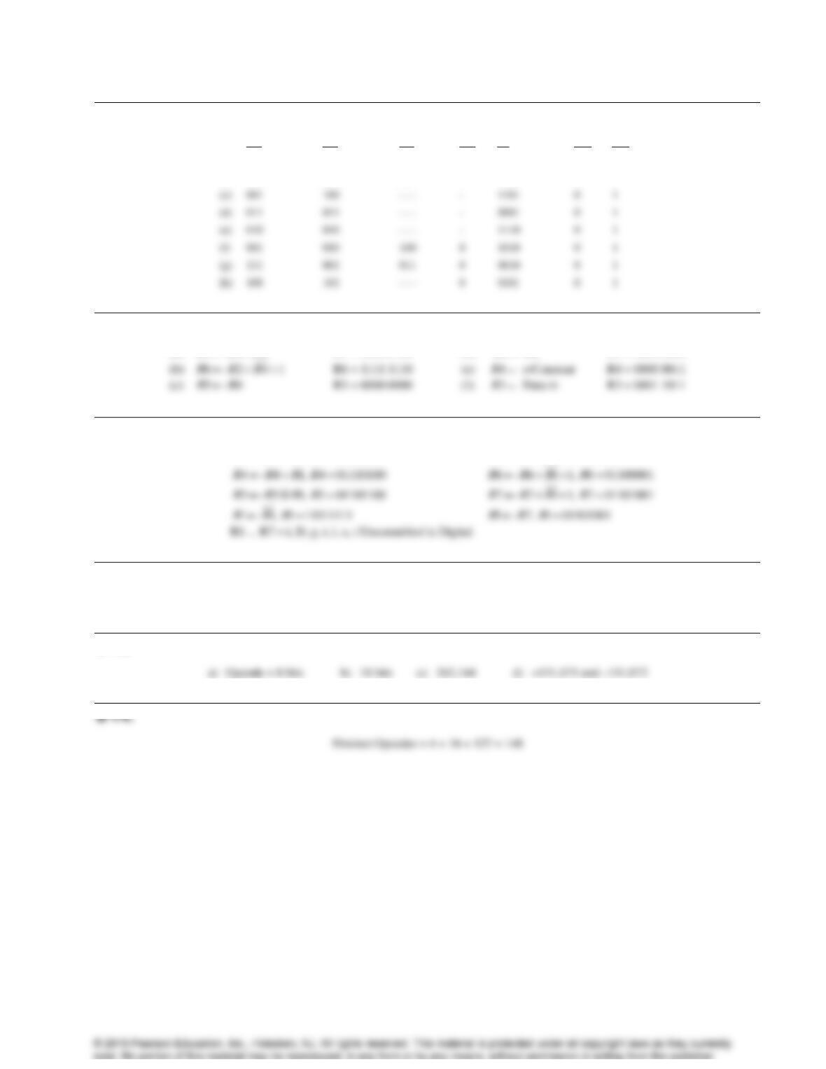
8-9.
DA
AA
BA
MB
FS
MD
RW
(a)
011
– – –
– – –
–
– – – –
1
1
(b)
100
000
000
0
1010
0
1
8-10.*
(a)
5 4 5R R R
R5 = 0000 0100 (d)
50RR
R5 = 0000 0000
50RR
8-11.
3 3 1, 3 01100111R R R R
1 1 1, 1 1100000R R R
8-12.
a) 64 b) 32 c) 0 to 65,535 d) –32,768 to +32,767
8-13.*
exist. No portion of this material may be reproduced, in any form or by any means, without permission in writing from the publisher.
(c)
001
100
– – –
–
1101
0
1
(d)
011
011
– – –
–
0001
0
1
(e)
010
010
– – –
–
1110
0
1
(f)
001
010
100
0
1010
0
1
(g)
111
001
011
0
0010
0
1
100
101
– – –
0
0101
0
1
Problem Solutions – Chapter 8
4
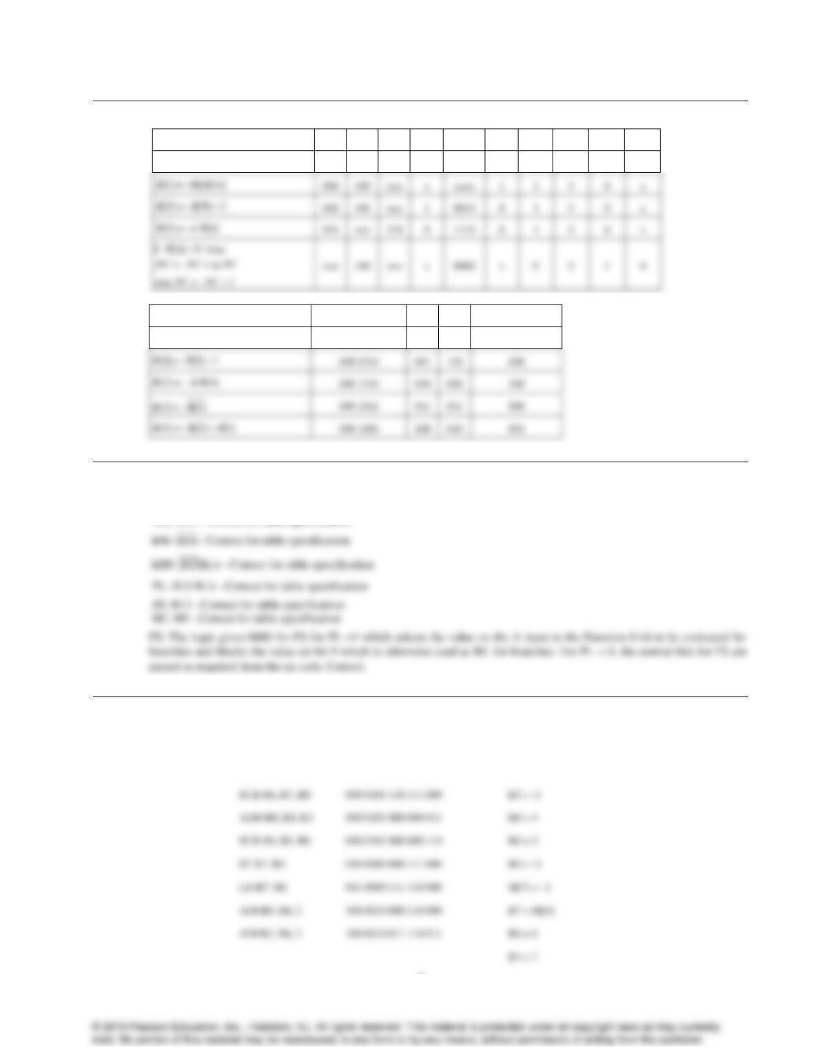
8-15.
Instruction Register Transfer
DA
AA
BA
MB
FS
MD
RW
MW
PL
JB
[0] [7] [3]R R R
000
111
011
0
1010
0
1
0
0
x
Instruction Register Transfer
Operation Code
DR
SA
SB or Operand
[0] [7] R[6]RR
000 0010
000
111
110
001
110
000
010
000
100
000 1001
100
010
001
8-16.
MB: B15 – Correct for table specification
MD: B13 – Correct for table specification
8-17.
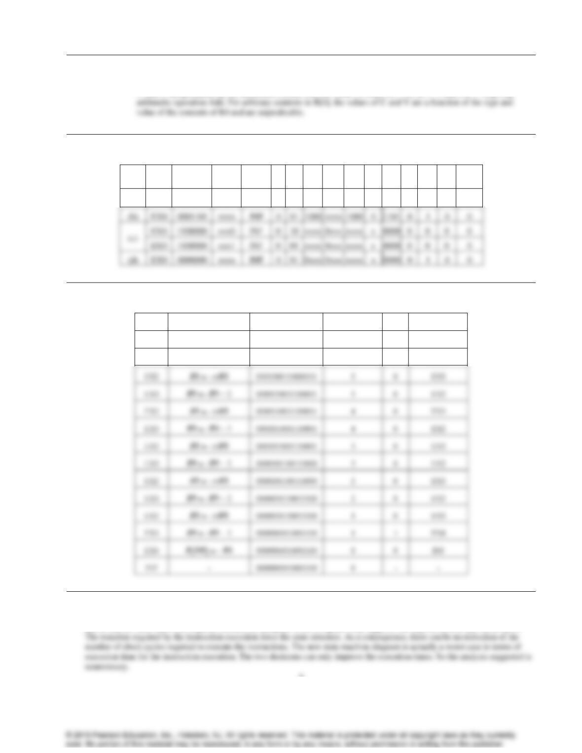
Instruction
Code
Registers/Memory changed
ADD R0, R1, R2
000 0101 000 001 010
SUB R3, R4, R5
000 001 011 100 101
R0 = 3
ADD R0, R0, R3
000 0101 000 000 011
R6 = 4
ST R7, R0
010 0000 000 111 000
R0 = -2
LD R7, R6
011 0000 111 110 000
M[7] = -2
ADI R3, R6, 3
100 0010 011 110 011
R0 = 6
R3 = 7
001
100
xxx
x
xxxx
1
1
0
0
x
010
101
xxx
1
0010
0
1
0
0
x
011
xxx
110
0
1110
0
1
0
0
x
Problem Solutions – Chapter 8
5
8-18.
[4] [4] [4]R R R
V and C are produced by the arithmetic circuit. For the XOR FS code, S1 = 0, S0 = 1. and Cin = 0, giving
8-19.
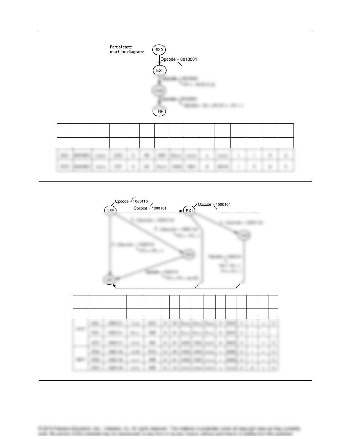
Part
State
Opcode
VCNZ
Next
State
IL
PS
DX
AX
BX
MB
FS
MD
RW
MM
MW
(a)
EX0
0000101
xxxx
EX1
0
01
0xxx
0xxx
0xxx
0
0101
0
1
0
0
8-20.
State
Instruction
R8
R9
Z
Next State
EX0
R8 RSA
0
EX1
EX1
R9 zfOP
0101100111000111
x
0
EX2
EX2
R8 srR8
0101100111000111
5
0
EX3
EX2
R8 srR8
0010110011100011
4
0
EX3
EX3
R9 R9 – 1
0001011001110001
4
0
EX2
EX2
R8 srR8
0001011001110001
3
0
EX3
EX3
R9 R9 – 1
0000101100111000
3
0
EX2
EX2
R8 srR8
0000101100111000
2
0
EX3
EX3
R9 R9 – 1
0000010110011100
2
0
EX2
EX2
R8 srR8
0000010110011100
1
0
EX3
EX3
R9 R9 – 1
0000001011001110
1
1
EX4
EX4
0000001011001110
0
0
INF
0000001011001110
0
8-21.+
Removal of the two decisions on zero operations does not affect the number of states in the state machine diagram. The reason for
this is that the same states are required because the datapath of the computer only supports one register transfer per clock cycle.
Problem Solutions – Chapter 8
6
8-22.
R8R SB
State
Opcode
VCNZ
Next
State
IL
PS
DX
AX
BX
MB
FS
MD
RW
MM
MW
EX0
0010001
xxxx
EX1
0
00
1000
xxxx
0xxx
0
1100
0
1
0
0
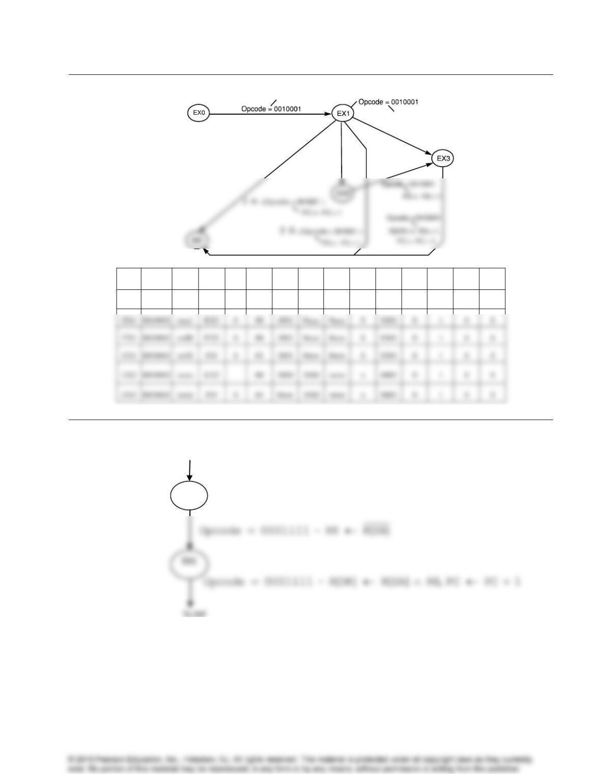
8-23.
R8 R8 R8
R8 R8
R DR R SA R SB +
Partial state machine diagram:
Part
State
Opcode
VCNZ
Next
State
IL
PS
DX
AX
BX
MB
FS
MD
RW
MM
MW
EX0
1000110
xxx0
EX3
0
00
1000
1000
xxxx
x
0000
0
1
x
0
EX3
1000110
xxxx
0
10
xxxx
xxxx
xxxx
x
xxxx
0
0
x
0
EX0
1000101
xxxx
EX1
0
00
0xxx
1000
1000
0
1010
0
1
x
0
Problem Solutions – Chapter 8
7
8-24.
R8 R8 R8
R9R SA R SB –
Z Opcode 0010001=
Partial state machine diagram:
State
Opcode
VCNZ
Next
State
IL
PS
DX
AX
BX
MB
FS
MD
RW
MM
MW
EX0
0010001
xxxx
EX1
0
00
1000
1000
1000
0
1010
0
1
0
0
8-25.
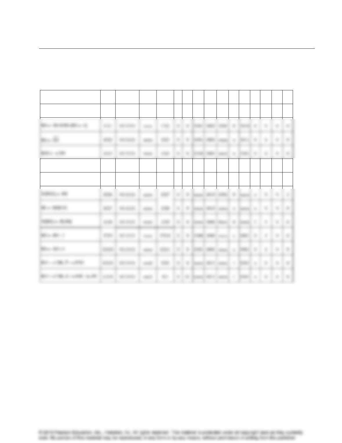
Partial state machine diagram, assuming the opcode for the new instruction is 0001111:
From INF
EX0
To INF
Problem Solutions – Chapter 8
8
8-26.
The operation code used for SMR and these instructions is 0111111 which is easy to generate by complementing all 0’s. The word
to be stored in memory is built in a register by complementing all 0’s and ANDing the result with the value of SB from the
original instruction. The register value generated is incremented, stored in memory and loaded into the IR after the execution of
each transfer from a register to a memory location.
Register Transfer
State
Opcode
VCNZ
Next
State
IL
PS
DX
AX
BX
MB
FS
MD
RW
MM
MW
R8 R[SA]
EX0
0111111
xxxx
EX1
0
00
1000
0xxx
xxxx
0
0000
1
1
0
0
R9 R10 zf SB
EX4
0111111
xxxx
EX5
0
0
1001
1010
xxxx
1
1000
0
1
0
0
R11 zf SB
EX5
0111111
xxxx
EX6
0
0
1011
xxxx
xxxx
1
1100
0
1
0
0
EX6
0111111
xxxx
EX7
0
0
xxxx
1010
1001
0
xxxx
x
0
0
1
EX7
0111111
xxxx
EX8
1
0
xxxx
1010
xxxx
x
xxxx
x
0
0
0
EX8
0111111
xxxx
EX9
0
0
xxxx
1000
0xxx
0
xxxx
1
1
0
0
EX9
0111111
xxxx
EX10
0
0
1000
1000
xxxx
x
0001
0
1
0
0
0111111
xxxx
EX11
0
0
1001
1001
xxxx
x
0001
0
1
0
0
0111111
xxx0
EX5
0
0
xxxx
1011
xxxx
1
0101
x
0
0
0
0111111
xxx1
0
01
xxxx
1011
xxxx
1
0101
x
0
0
0
EX1
0111111
xxxx
EX2
0
0
1001
1001
1001
0
1010
0
1
0
0
EX2
0111111
xxxx
EX3
0
0
1001
1001
xxxx
x
1011
0
1
0
0
EX3
0111111
xxxx
EX4
0
0
1010
1001
xxxx
x
1101
0
0
0
0
Problem Solutions – Chapter 8
9
8-27.
Since the condition codes are not fully available to the programmer (only N and Z are used by instructions, not V and C), the approach
of problem 6-1, part c, for a signed comparison using the N and V bits is not possible. Instead the program must make the comparisons
based upon the signs of the current minimum value and the current array element.
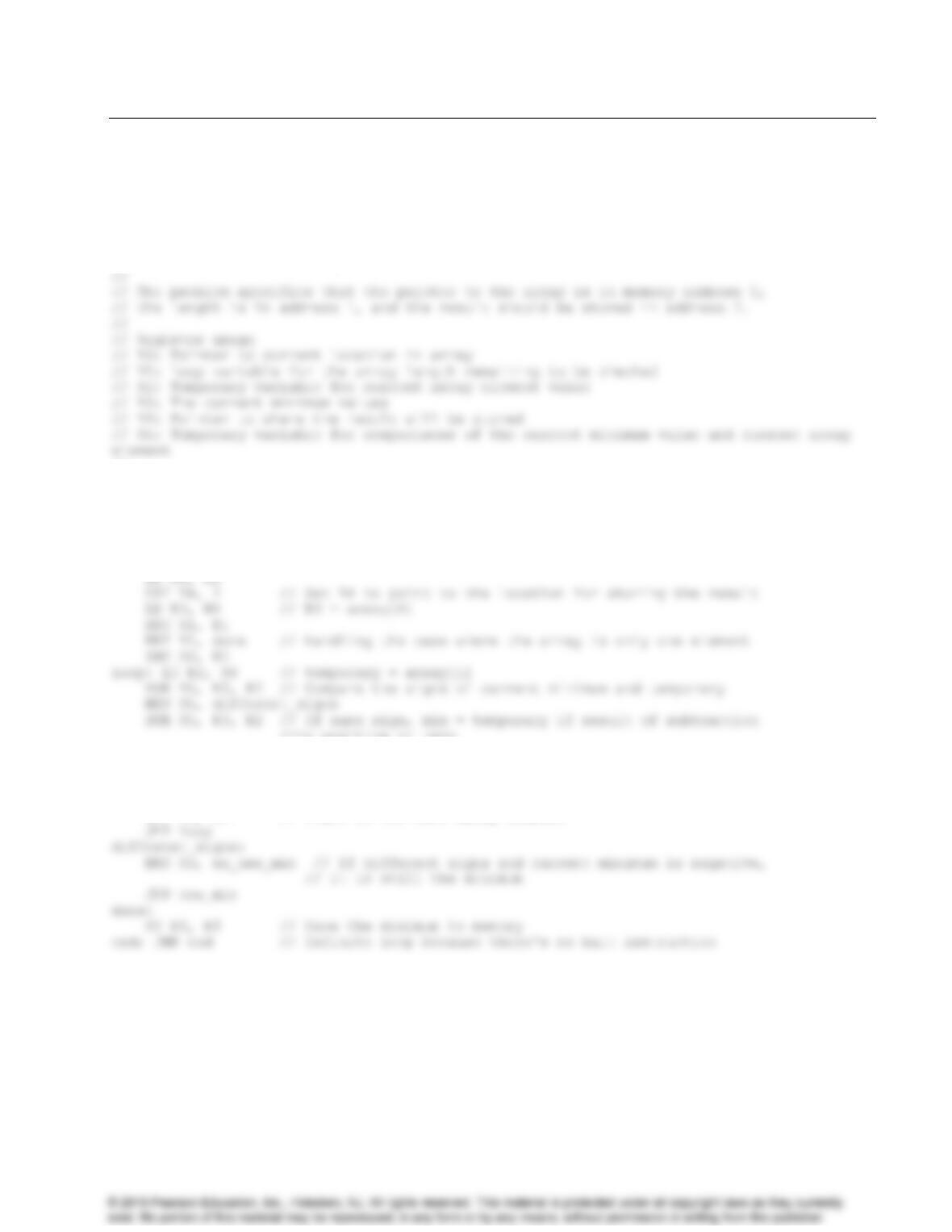
// Assembly for the solution to problem 8-27
// Logic and Computer Design Fundamentals, 5th edition
//
// Using labels for locations to make the targets of branches and jumps more clear
LDI R0, 0 // Read in pointer to array and its length
LDI R1, 1
LD R0, R0
//is positive or zero
BRN no_new_min
new_min: MOV R3, R2
no_new_min: DEC R1, R1 // Update loop variable
BRZ R1, done
INC R0, R0 // Point to the next array element