Problem Solutions – Chapter 6
1
CHAPTER 6
© 2016 Pearson Education, Inc.
6-1.
(a) R1 + 2’s complement of R2 = 2n + R1 – R2. If R1 R2, the result is 2n. The 2n gives C = 1.
R1 + 2’s complement of R2 = 2n + R1 – R2, if R1 < R2, the result is < 2n giving C = 0.
6-2.*
1001 1001
6-3.
6-4.*
sl 1001 0100 sr 0110 0101
6-5.*
6-6.*
a) 1000, 0100, 0010, 0001, 1000. …
Problem Solutions – Chapter 6
2
6-7.
a) 000, 100, 110, 111, 011, 001, 000, …
b) # States = 2n
6-8.
6-9.+
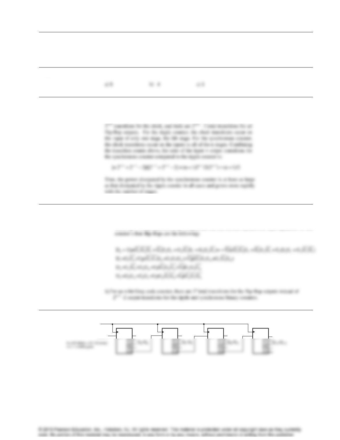
Examine an n-bit ripple counter and an n-bit synchronous counter. If
either of these counters cycles through all of its states, there are 2(2n) =
6-10.
a) Assuming there is an input “Up” for which the Gray code counter counts up when Up = 1 and down
when Up = 0, and that the counter outputs are G3, G2, G1, and G0, then the input equations for the
6-11.
EN Q0
CTR 4
EN Q0
CTR 4
EN Q0
CTR 4
CLK
Count
EN Q0
CTR 4
Problem Solutions – Chapter 6
3
6-12.
Load
CTR 4
CLK
Load
CTR 4
CLK
6-13.
Load
CTR 4
Load
CTR 4
Clk
Init
6-14. *
The equations given on page 352 can be manipulated into SOP form as follows:
11
D Q ,
2 2 1 8 1 2 8 1 2 2 8
D Q Q Q Q Q Q Q Q Q Q ,
4 4 1 2 1 2 4 1 4 2 4
D Q Q Q Q Q Q Q Q Q Q ,
8 8 1 8 1 2 4 8 1 8 1 2 4 8 1 8 1 2 4 1 2
D Q (Q Q Q Q Q ) Q (Q Q Q Q Q ) Q (Q Q )(Q Q Q ) Q Q
4 8 1 8
Q Q Q Q .
These equations are mapped onto the K-maps for Table 6-9 below and meet the specifications given by the maps and the
table.
Q2
1
Q2
0
1
0
0
0
1
1
D1D2
D
C
D
C
EN
Y
Q1
Q2
Problem Solutions – Chapter 6
4
6-15. *
Present
state
Next
state
A
B
C
A
B
C
0
0
0
1
a)
B
DC
C
D B C
b)
A
D BC AC
B
D ABC BC
C
DC
6-16.
Present state
Next state
A
B
C
A
B
C
0
0
0
0
0
1
0
0
1
1
0
1
A
D AB AC ABC
B
DB
C
D BC BC
6-17.
The basic cell of the register is as follows:
6-18.
: 1 2
X R R
6-19.*
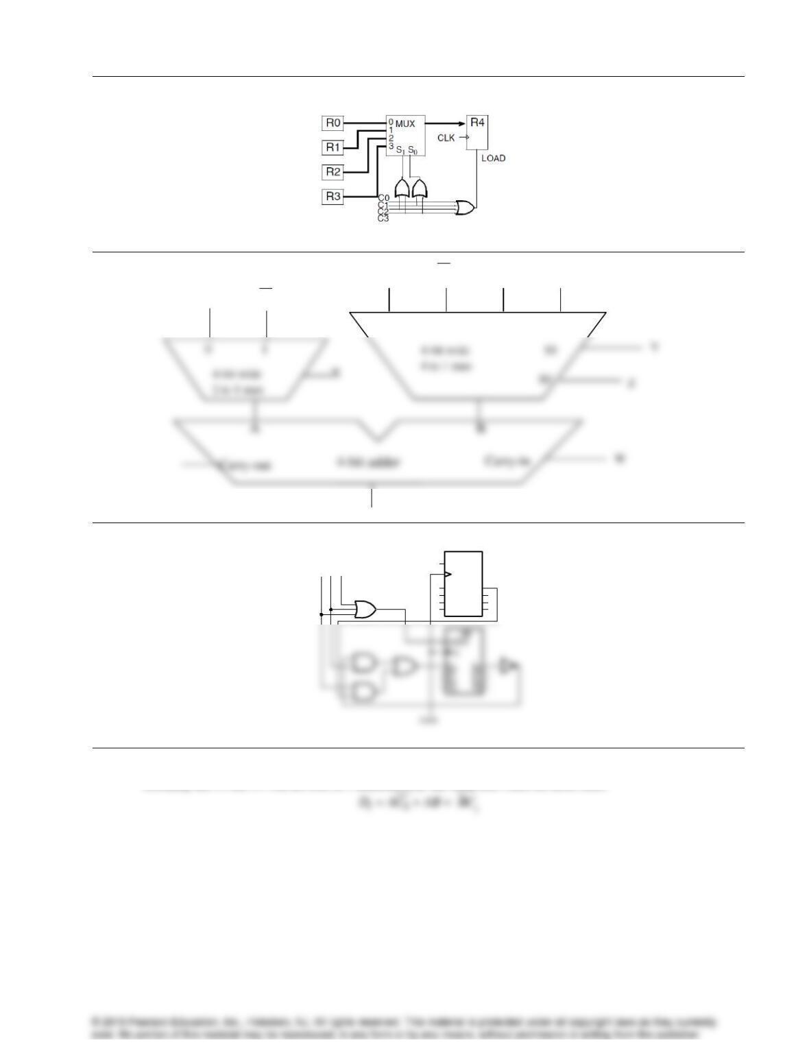
R1 R2
Problem Solutions – Chapter 6
5
6-20.
6-21.
6-22.*
LOAD
Q0
Q1
Q2
Q3
C
R1
D0
D1
D2
D3
C2C1C0
6-23.
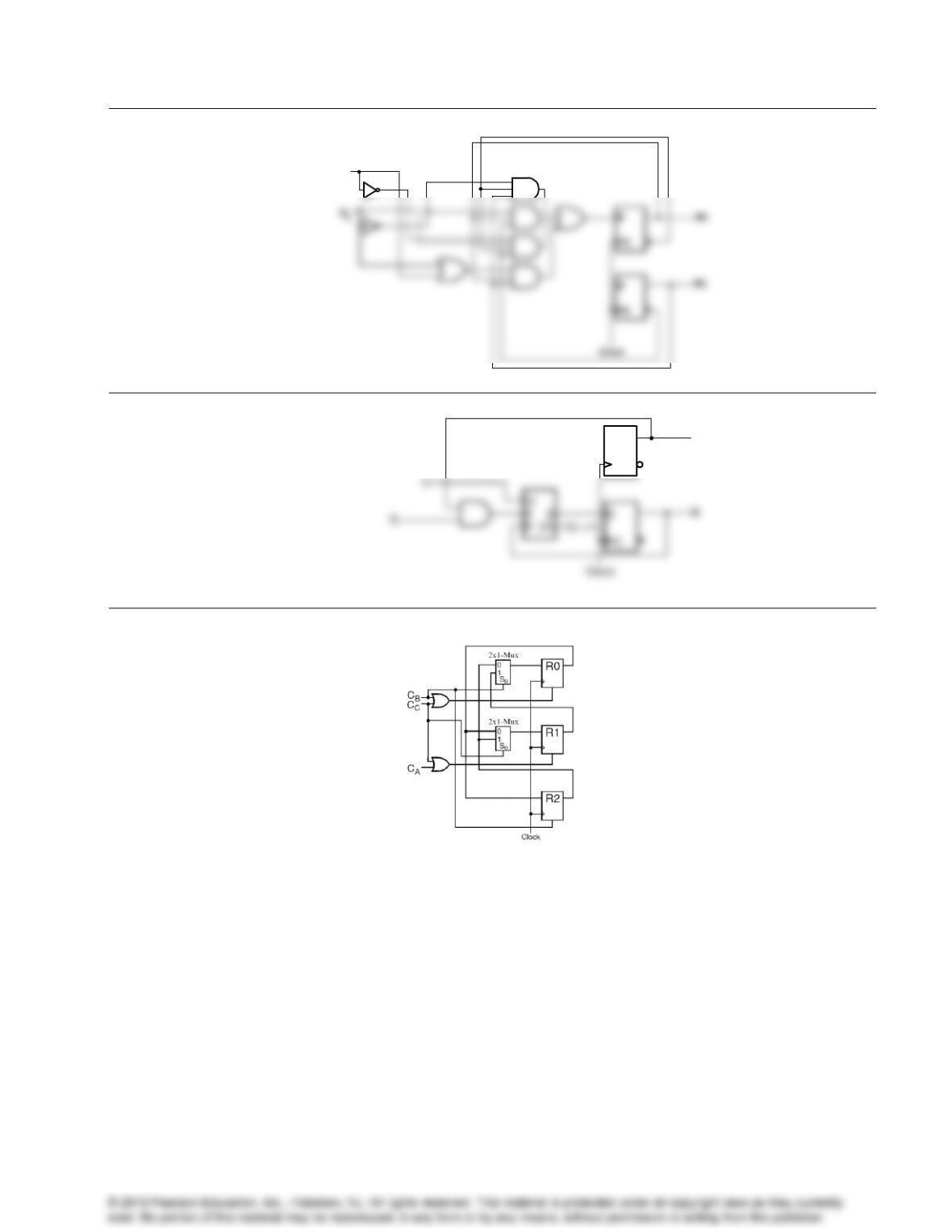
Assuming that C1 and C0 will not both be 1 simultaneously and using don’t cares for those cases:
R1 R1
F
R2 R2 R1 1111
0 1 2 3
0 1
Z
Y
W
Problem Solutions – Chapter 6
6
6-24.
6-25.
D
C
A
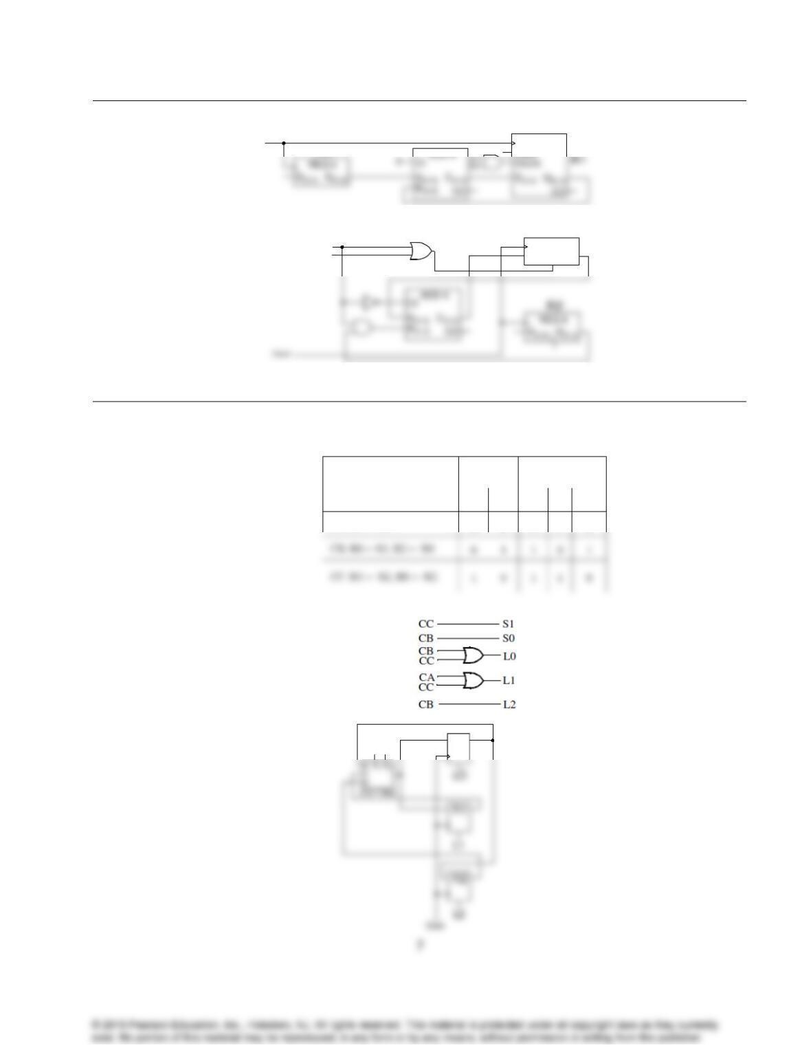
Ci = S0 for lowest order bit.
6-26.
0
S
1
Problem Solutions – Chapter 6
6-27.*
CTR 4
CLK
C1
R2
a)
b)
Q(0-3)
REG 4
D(0-3)
R1
L
C1
C2
6-28.
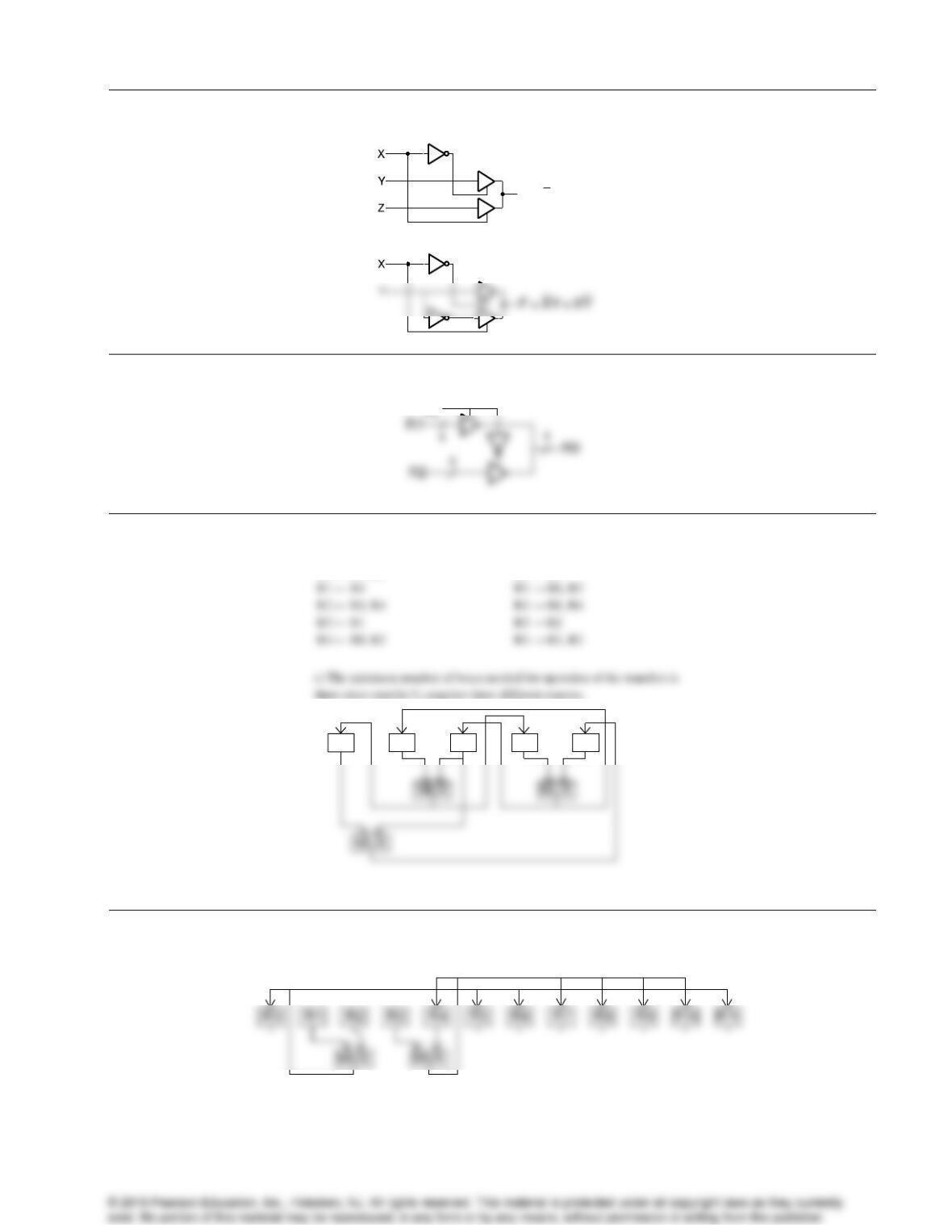
The register transfer logic is as follows:
Operation
Select
Load
S1
S0
L0
L1
L2
CA: R1 ← R0
0
0
0
1
0
CC: R1 ← R2, R0 ← R2
R0
Problem Solutions – Chapter 6
8
6-29.
a)
b)
H = XY + XZ
6-30.
Replace multiplexer with:
6-31.*
a) Destination ← Source Registers
R0 ← R1, R2
b) Source Registers → Destination
R0 → R4
R0
R1 R2 R3 R4
d)
6-32.
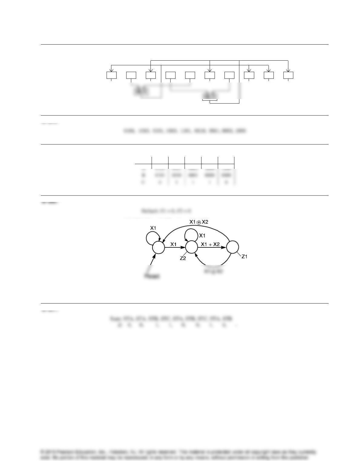
a) Using two clock cycles, the minimum # of buses is 2 .
b)
Problem Solutions – Chapter 6
9
6-33.
R0 R1 R2 R3 R4 R5 R6 R7 R8 R9
Two clock cy cles minimum
6-34.*
6-35.*
Shifts:
0
1
2
3
4
0
1
1
1
0
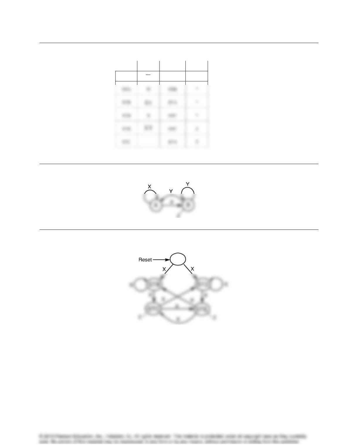
S0
S1 S2
Def ault: Z1 0, Z2 0
·X2
Problem Solutions – Chapter 6
10
6-38.
State
Input
Next State
Output
STA
W
STA
*
*Default: Z = 0
6-39.
Default: Z = 0
6-40.*
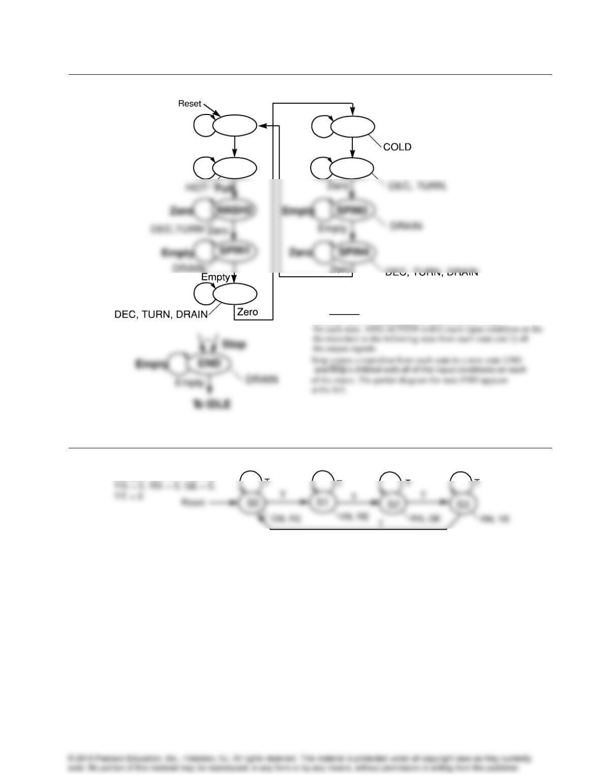
Default: Z = 0
STA
0
Problem Solutions – Chapter 6
11
6-41.+
6-42.
Def ault: GN = 0, RE = 0,
a)
Default: HOT = 0,
IDLE
DEC = 0, TURN = 0,
DRAIN = 0, COLD = 0,
W
A
SH1
W
A
SH2
SPIN1
SPIN3
Zero
Empty
Zero
Empty
Full
SPIN2
RINSE1
RINSE2
Start
Start
Full
Full
Zero
Zero
Full
OR
ACTION
with each input condition on the “loop”
for each state. AND ACTION with1) each input condition on the
the transition to the following state from each state and 2) all
the output signals.
of the states. The partial diagram for state END appears
at the left.
IDLE
Stop
b) Add a flip-flop called ACTION controlled by Pause and Start.
The flip-flop is set by STAR
T
and reset by Pause.
Load = 0.