Chapter 13
Fabrication of Microelectronic,
Micromechanical, and
Microelectromechanical Devices;
Nanomanufacturing
Questions
13.1 Define the terms wafer, chip, device, integrated
(2) simple electronic element such as a transis-
13.2 Why is silicon the most commonly used semi-
conductor in IC technology? Explain.
The reason is its unique capabilities regarding
13.3 What do the terms VLSI, IC, CVD, CMP, and
DIP stand for?
13.4 How do n-type and p-type dopants differ? Ex-
deposition?
strate.
13.6 Comment on the differences between wet and
dry etching.
isotropic etch patterns, and is relatively easy to
© 2008 Pearson Education, Inc., Upper Saddle River, NJ. All rights reserved.
This material is protected by Copyright and written permission should be obtained from the publisher prior to any prohibited
reproduction, storage in a retrieval system, or transmission in any form or by any means, electronic, mechanical, photocopying, recording, or
likewise. For information regarding permission(s), write to:
Rights and Permissions Department, Pearson Education, Inc., Upper Saddle River, NJ 07458.
13.7 How is silicon nitride used in oxidation?
13.8 What are the purposes of prebaking and post-
baking in lithography?
done (prior to lithography) to remove solvent
13.9 Define selectivity and isotropy and their impor-
tance in relation to etching.
13.10 What do the terms linewidth and registration
refer to?
13.11 Compare diffusion and ion implantation.
Diffusion and ion implantation are similar. Dif-
fusion refers to the process of atom migration,
and is closely related to temperature. Ion im-
plantation involves accelerating ions and direct-
ing them to a surface where they are incorpo-
rated. Thus, both diffusion and ion implanta-
tion can be used to drive dopants into semicon-
ductor materials.
13.12 What is the difference between evaporation and
sputtering?
then condense on the workpiece. A further de-
13.13 What is the definition of yield? How important
is yield? Comment on its economic significance.
13.14 What is accelerated life testing? Why is it prac-
ticed?
long time, and thus it would not be practical to
chanical features on silicon or on other surfaces.
As shown in Fig. 13.34, surface micromachining
involves production of a desired feature through
film deposition and etching; a spacer layer is
then removed through wet etching, where the
spacer layer is easily etched while the structural
material is not etched.
13.17 What is LIGA? What are its advantages over
other processes?
© 2008 Pearson Education, Inc., Upper Saddle River, NJ. All rights reserved.
This material is protected by Copyright and written permission should be obtained from the publisher prior to any prohibited
reproduction, storage in a retrieval system, or transmission in any form or by any means, electronic, mechanical, photocopying, recording, or
likewise. For information regarding permission(s), write to:
Rights and Permissions Department, Pearson Education, Inc., Upper Saddle River, NJ 07458.
LIGA-produced structure is a mold for further
13.18 What is the difference between isotropic and
anisotropic etching?
mask can be produced from a variety of mate-
sisted ion etching and dry plasma etching?
13.21 Which process(es) in this chapter allow(s) fab-
rication of products from polymers? (See also
Chapter 10.)
By the student. It will be noted that poly-
mers are most easily produced from LIGA and
solid freeform fabrication processes. They can
13.23 With an appropriate sketch, describe the ther-
stitching, a gold wire is welded to a bond pad
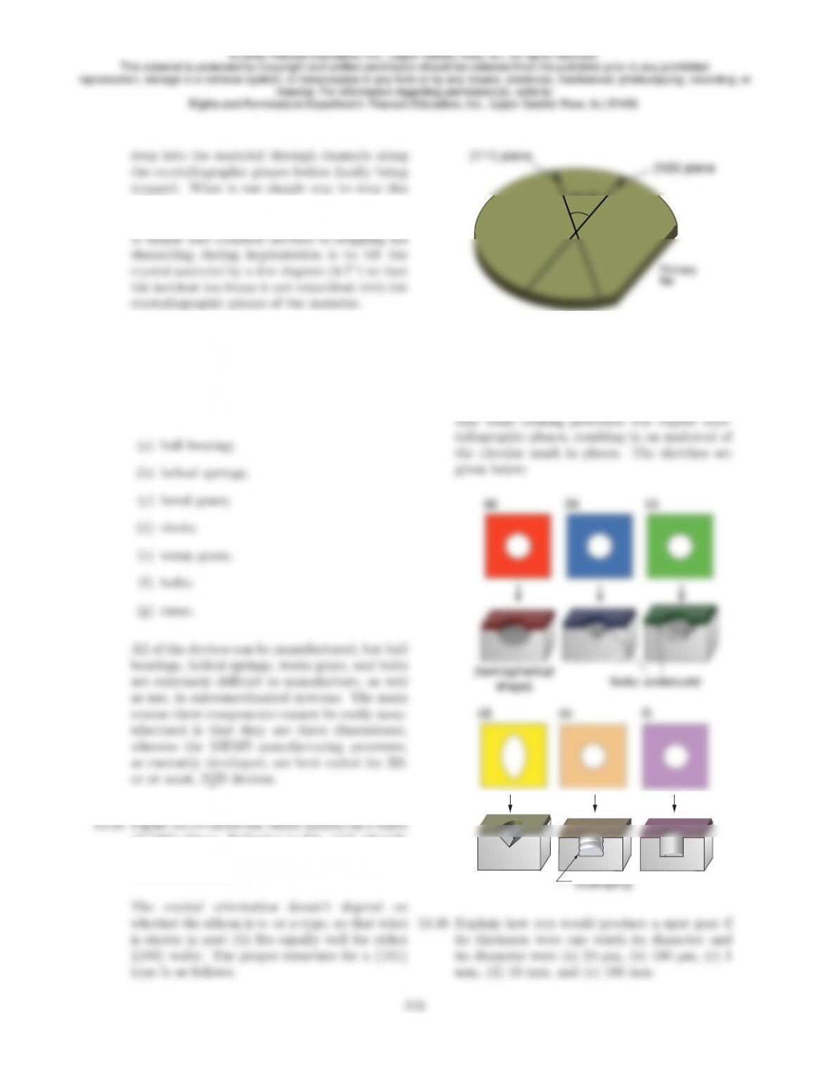
13.25 Why are flats or notches machined onto silicon
wafers? Explain.
and to also indicate the crystallographic orien-
electrical connections are very difficult to make
if all of the connections must lie within a single
plane. A via allows the designer to make elec-
trical connections on a number of planes, thus
greatly simplifying layout on a board.
13.27 What is a flip chip? Describe its advantages
© 2008 Pearson Education, Inc., Upper Saddle River, NJ. All rights reserved.
This material is protected by Copyright and written permission should be obtained from the publisher prior to any prohibited
reproduction, storage in a retrieval system, or transmission in any form or by any means, electronic, mechanical, photocopying, recording, or
likewise. For information regarding permission(s), write to:
Rights and Permissions Department, Pearson Education, Inc., Upper Saddle River, NJ 07458.
13.28 Explain how IC packages are attached to a
printed circuit board if both sides will contain
ICs.
13.29 In a horizontal epitaxial reactor (see the accom-
panying figure), the wafers are placed on a stage
(susceptor) that is tilted by a small amount,
usually 1◦-3◦. Why is this procedure done?
The stage in the horizontal epitaxial reactor is
usually tilted by a small amount to provide
equal amounts of reactant gases in both the
front and back of the chamber. If the stage
is not tilted, the reactant gases would be par-
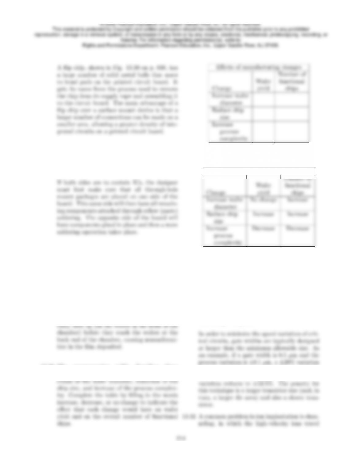
13.30 The accompanying table describes three
changes in the manufacture of a wafer: in-
crease of the wafer diameter, reduction of the
complexity
The completed table is shown below:
Effects of manufacturing changes
13.31 The speed of a transistor is directly propor-
tional to the width of its polysilicon gate, with
a narrower gate resulting in a faster transistor
and a wider gate resulting in a slower transistor.
Knowing that the manufacturing process has a
certain variation for the gate width, say ±0.1
µm, how might a designer alter the gate size of
a critical circuit in order to minimize its speed
variation? Are there any penalties for making
this change? Explain.
in speed would be expected. However, if the
gate width is increased to 0.8 µm, the speed
© 2008 Pearson Education, Inc., Upper Saddle River, NJ. All rights reserved.
This material is protected by Copyright and written permission should be obtained from the publisher prior to any prohibited
reproduction, storage in a retrieval system, or transmission in any form or by any means, electronic, mechanical, photocopying, recording, or
likewise. For information regarding permission(s), write to:
Rights and Permissions Department, Pearson Education, Inc., Upper Saddle River, NJ 07458.
effect?
13.33 The MEMS devices described in this chapter
use macroscale machine elements, such as spur
gears, hinges, and beams. Which of the follow-
ing machine elements can or cannot be applied
to MEMS, and why?
54.74°
13.35 Referring to Fig. 13.23, sketch the holes gener-
ated from a circular mask.
The challenge to this problem is that conical
sections are difficult to sketch. Note, however,
© 2008 Pearson Education, Inc., Upper Saddle River, NJ. All rights reserved.
This material is protected by Copyright and written permission should be obtained from the publisher prior to any prohibited
reproduction, storage in a retrieval system, or transmission in any form or by any means, electronic, mechanical, photocopying, recording, or
likewise. For information regarding permission(s), write to:
Rights and Permissions Department, Pearson Education, Inc., Upper Saddle River, NJ 07458.
(b) 100 µm spur gear could be produced
through micromachining; if silicon is not
(e) 100 mm gear could best be machined (see
Class-1?
room.
13.38 Describe the difference between a microelec-
tronic device, a micromechanical device and
ing a micromechanical device and integrated mi-
13.39 Why is silicon often used with MEMS and
MEMS devices?
13.40 Explain the purpose of a spacer layer in surface
micromachining.
13.41 What do the terms SIMPLE and SCREAM
SIMPLE stands for silicon micromachining
13.42 Which process(es) in this chapter allow the fab-
rication of products from ceramics? (See also
Chapter 11.)
By the student. Note that ceramic products are
13.44 Describe the differences between stereolithogra-
phy and microstereolithography.
in Section 13.16, microstereolithography uses
© 2008 Pearson Education, Inc., Upper Saddle River, NJ. All rights reserved.
This material is protected by Copyright and written permission should be obtained from the publisher prior to any prohibited
reproduction, storage in a retrieval system, or transmission in any form or by any means, electronic, mechanical, photocopying, recording, or
likewise. For information regarding permission(s), write to:
Rights and Permissions Department, Pearson Education, Inc., Upper Saddle River, NJ 07458.
13.45 Lithography produces projected shapes; conse-
three-dimensional shapes, such as lenses?
13.46 List and explain the advantages and limitations
of surface micromachining as compared to bulk
micromachining.
•Very good dimensional tolerances.
•Complex shapes in multiple layers.
ers.
•The process is effectively limited to silicon
as the substrate material.
•Wet etchants can result in structures that
13.47 What are the main limitations to the LIGA pro-
cess?
13.48 Describe the process(es) that can be used to
make the microtweezers shown in Fig. 13.49
other than HEXSIL.
compliant and lightweight structure. Although
processes such as SCREAM (pp. 855-857) can
be used, the required aspect ratio will be diffi-
bers to aid in molding. However, a structure
that serves the same function can be produced,
even though vertical sidewalls cannot be pro-
duced.
13.49 A certain wafer manufacturer produces two
equal-sized wafers, one containing 500 chips and
the other containing 300 chips. After testing, it
are defective. What are the yields of the two
wafers? Can any relationship be established be-
tween chip size and yield?
© 2008 Pearson Education, Inc., Upper Saddle River, NJ. All rights reserved.
This material is protected by Copyright and written permission should be obtained from the publisher prior to any prohibited
reproduction, storage in a retrieval system, or transmission in any form or by any means, electronic, mechanical, photocopying, recording, or
likewise. For information regarding permission(s), write to:
Rights and Permissions Department, Pearson Education, Inc., Upper Saddle River, NJ 07458.
50)/300 = 83.3%. Thus, given the same num-
ber of defects per wafer, the wafer with smaller
chips (i.e., more chips per wafer) will have a
13.50 A chlorine-based polysilicon etch process dis-
resist and exposed oxide will be consumed in
etching 350 nm of polysilicon? What should
the polysilicon:oxide selectivity be in order to
remove only 4 nm of exposed oxide?
13.51 During a processing sequence, four silicon-
dioxide layers are grown by oxidation: 400 nm,
150 nm, 40 nm, and 15 nm. How much of the
silicon substrate is consumed?
13.6, the ratio of oxide to the amount of silicon
13.52 A certain design rule calls for metal lines to be
no less than 2 µm wide. If a 1 µm-thick metal
layer is to be wet etched, what is the minimum
photoresist width allowed? (Assume that the
wet etch is perfectly isotropic.) What would be
the minimum photoresist width if a perfectly
anisotropic dry-etch process were used?
A perfectly isotropic wet-etch process will etch
equally in the vertical and horizontal directions.
Therefore, the wet-etch process requires a min-
imum photoresist width of 2 µm, plus 1 µm per
side, to allow for the undercutting, hence a to-
2µ.
13.53 Using Fig. 13.18, obtain mathematical expres-
sions for the etch rate as a function of temper-
Direc- 1/T Etch rate ln(Etch
3.3 4 1.386
h100i2.55 70 4.248
3.3 2 0.6931
h111i2.55 2 0.6931
3.3 0.015 -4.200
ln(y) vs. 1/T curve, and bis the y-intercept.
From the data in the table above, we can ob-
tain the following
h111i-6.524 17.33
in the h100idirection:
y=1.236 ×10⁷e−4.74/T
in the h111idirection:
y=3.3×10⁷e−6.524/T
13.54 If a square mask of side length 100 µm is
placed on a {100}plane and oriented with a
side in the h110idirection, how long will it
take to etch a hole 4 µm deep at 80◦C using
ethylene-diamine/pyrocatechol? Sketch the re-
© 2008 Pearson Education, Inc., Upper Saddle River, NJ. All rights reserved.
This material is protected by Copyright and written permission should be obtained from the publisher prior to any prohibited
reproduction, storage in a retrieval system, or transmission in any form or by any means, electronic, mechanical, photocopying, recording, or
likewise. For information regarding permission(s), write to:
Rights and Permissions Department, Pearson Education, Inc., Upper Saddle River, NJ 07458.
bottom as a function of time for the mask shown
in Fig. 13.17b.
or
x=ht
and (9.13).
W=18.998g/mole
6.023 ×10²³atoms/mole
= 1.62 ×10⁻¹² s
13.57 Calculate the undercut in etching a 10-µm-deep
The following table can now be constructed:
made of silicon oxide?
© 2008 Pearson Education, Inc., Upper Saddle River, NJ. All rights reserved.
This material is protected by Copyright and written permission should be obtained from the publisher prior to any prohibited
reproduction, storage in a retrieval system, or transmission in any form or by any means, electronic, mechanical, photocopying, recording, or
likewise. For information regarding permission(s), write to:
Rights and Permissions Department, Pearson Education, Inc., Upper Saddle River, NJ 07458.
Time to
etch
Etch 10 µm SiO2Observed
rate trench removed Ref. undercut
Etchant (µm/min) (min) (nm) (nm) (nm)
HF:HNO3: 20 0.5 15 10000 9985
CH3COOH
KOH 2 5 50 100 50
EDP 0.75 13.33 2.66 280 277
N(CH3)4OH 1.5 6.67 0.667 20 19.3
SF60.5 20 0 0 0
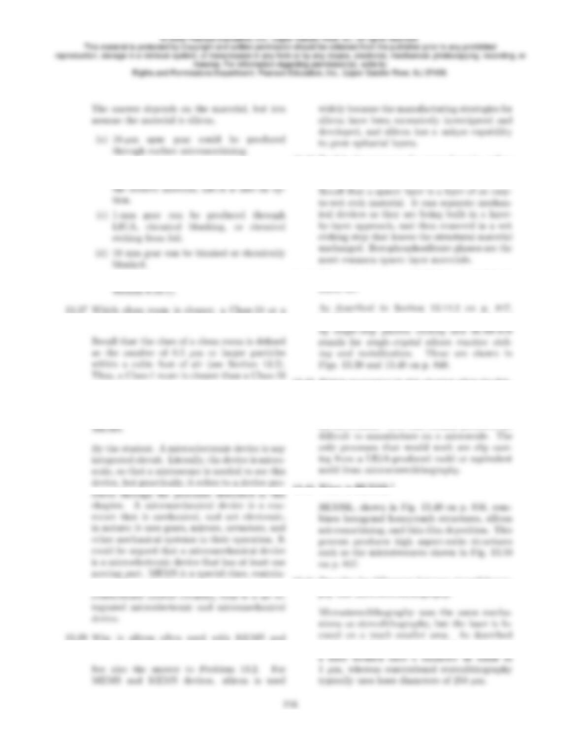
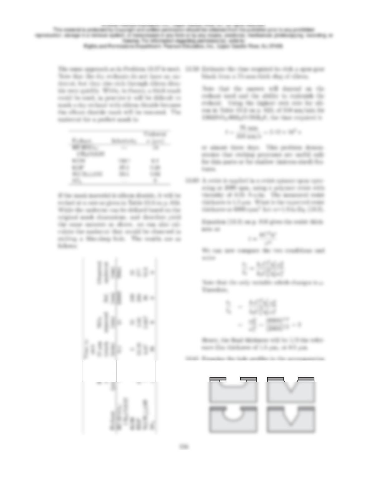
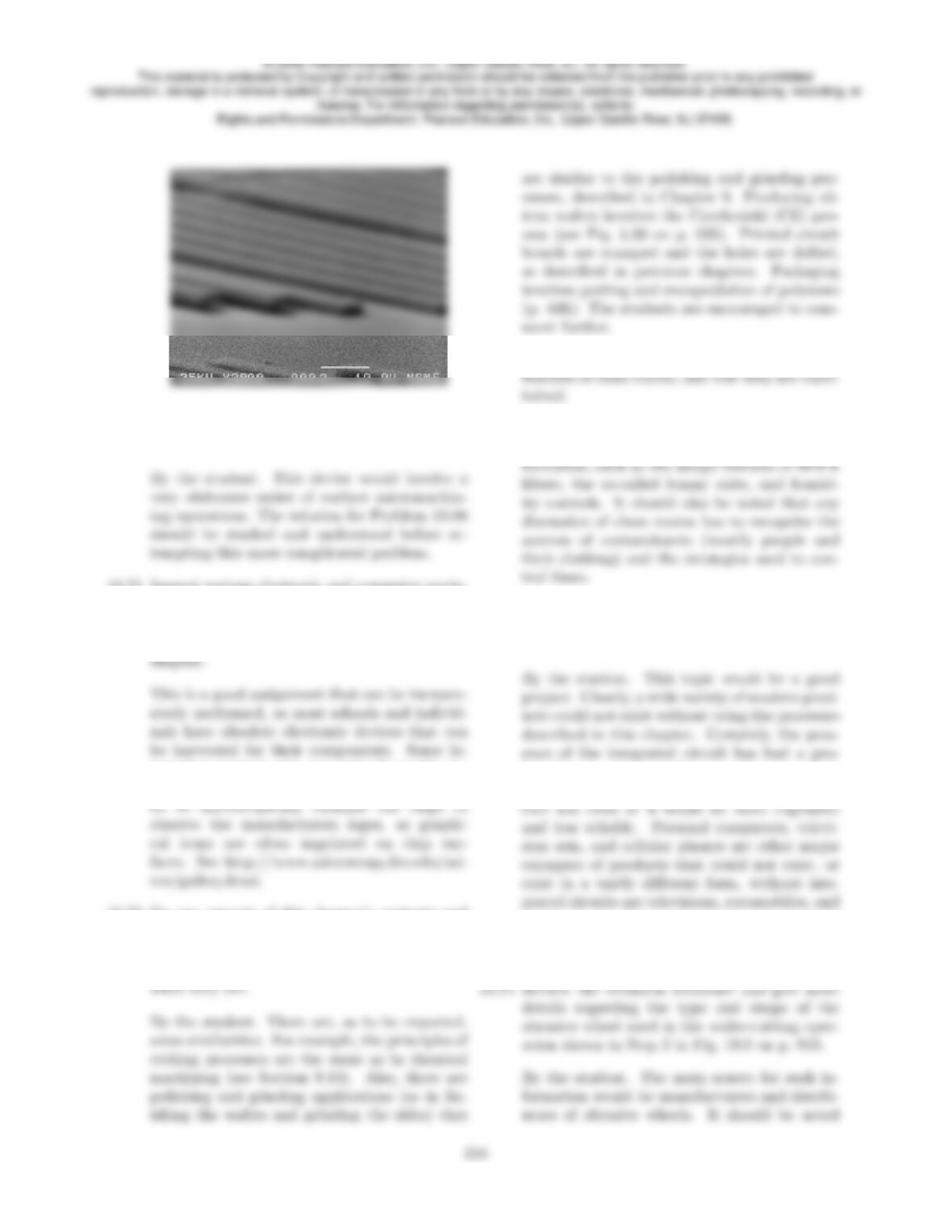
13.61 Examine the hole profiles in the accompanying
figure and explain how they might be produced.
© 2008 Pearson Education, Inc., Upper Saddle River, NJ. All rights reserved.
This material is protected by Copyright and written permission should be obtained from the publisher prior to any prohibited
reproduction, storage in a retrieval system, or transmission in any form or by any means, electronic, mechanical, photocopying, recording, or
likewise. For information regarding permission(s), write to:
Rights and Permissions Department, Pearson Education, Inc., Upper Saddle River, NJ 07458.
Fig. 13.23 on p. 831 to understand this solution
below. We can state the following:
from the dimensions given, but there is ei-
Fig. 13.17a on p. 824).
(b) The crystal workpiece is aligned so
that has undercut the mask. Compared
to the top right figure, this figure suggests
13.62 A polyimide photoresist requires 100 mJ/cm2
per µm of thickness in order to develop prop-
erly. How long does a 150 µm film need to
develop when exposed by a 1000 W/m2light
source?
t=1000 Nm
1000 W h= 150 s
13.63 How many levels are required to produce the
micromotor shown in Fig. 13.22d?
•Pin or bearing (it must protrude past the
rotor).
13.64 It is desired to produce a 500µm by 500 µm
diaphragm, 25 µm thick, in a silicon wafer 250
a proper opening with a diffusion bonding step
such as shown in part 3 of Fig. 13.41a on p. 849.
Using a wet etchant, a cavity as shown in part
2 of Fig. 13.41a will be produced, with an in-
© 2008 Pearson Education, Inc., Upper Saddle River, NJ. All rights reserved.
This material is protected by Copyright and written permission should be obtained from the publisher prior to any prohibited
reproduction, storage in a retrieval system, or transmission in any form or by any means, electronic, mechanical, photocopying, recording, or
likewise. For information regarding permission(s), write to:
Rights and Permissions Department, Pearson Education, Inc., Upper Saddle River, NJ 07458.
13.65 If the Reynolds number for water flow through
a pipe is 2000, calculate the water velocity if
turbulent or laminar? Explain.
η
where vis the velocity, Dis the channel diame-
If the channel diameter is 10 mm, then
(0.01)(1000) = 0.178 m/s
(0.0001)(1000) = 17.8 m/s
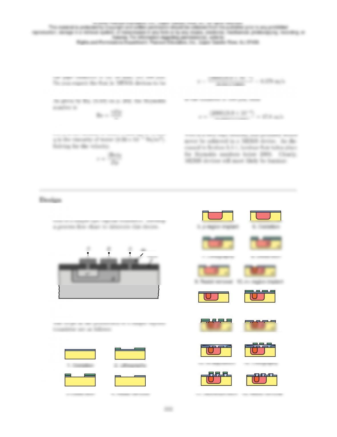
13.66 The accompanying figure shows the cross sec-
3 Oxide etch 4. Resist removal
n
pn
p
17. Aluminum etch 18. Resist removal
222
© 2008 Pearson Education, Inc., Upper Saddle River, NJ. All rights reserved.
This material is protected by Copyright and written permission should be obtained from the publisher prior to any prohibited
reproduction, storage in a retrieval system, or transmission in any form or by any means, electronic, mechanical, photocopying, recording, or
likewise. For information regarding permission(s), write to:
Rights and Permissions Department, Pearson Education, Inc., Upper Saddle River, NJ 07458.
13.67 Referring to the MOS transistor cross section in
the accompanying figure and the given table of
design rules, what is the smallest transistor size
Wobtainable? Which design rules, if any, have
no impact on the magnitude of W? Explain.
R1
R3 R2
R4 R6 R5
W
metal spacing
The smallest transistor size, W, that can be
obtained using the given design rule is:
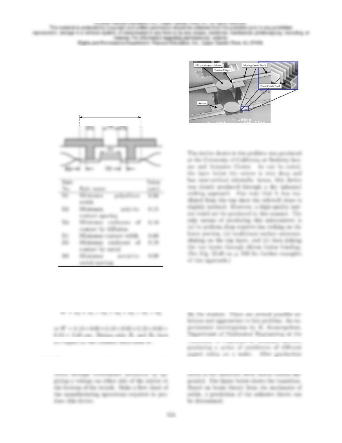
13.68 The accompanying figure shows a mirror that
is suspended on a torsional beam; it can be in-
The device shown in the problem was produced
at the University of California at Berkeley Sen-
sor and Actuator Center. As can be noted,
the layer below the mirror is very deep and
has near-vertical sidewalls; hence, this device
of this approach.)
13.69 Referring to Fig. 13.36, design an experiment to
find the critical dimensions of an overhanging
cantilever that will not stick to the substrate.
through surface micromachining, followed by
rinsing, some of the cantilevers attach them-
© 2008 Pearson Education, Inc., Upper Saddle River, NJ. All rights reserved.
This material is protected by Copyright and written permission should be obtained from the publisher prior to any prohibited
reproduction, storage in a retrieval system, or transmission in any form or by any means, electronic, mechanical, photocopying, recording, or
likewise. For information regarding permission(s), write to:
Rights and Permissions Department, Pearson Education, Inc., Upper Saddle River, NJ 07458.
13.70 Explain how you would manufacture the device
shown in Fig. 13.32.
13.71 Inspect various electronic and computer equip-
ment, take them apart as much as you can, and
identify components that may have been man-
ufactured by the techniques described in this
teresting projects also can arise from this ex-
periment. One project, for example, would
13.72 Do any aspects of this chapter’s contents and
the processes described bear any similarity to
the processes described throughout previous
chapters in this book? Explain and describe
are similar to the polishing and grinding pro-
cesses, described in Chapter 9. Producing sil-
icon wafers involves the Czochralski (CZ) pro-
cess (see Fig. 5.30 on p. 235). Printed circuit
boards are stamped and the holes are drilled,
as described in previous chapters. Packaging
involves potting and encapsulation of polymers
(p. 636). The students are encouraged to com-
ment further.
13.73 Describe your understanding of the important
Clean rooms are described in Section 13.2. Stu-
dents are encouraged to search for additional in-
13.74 Describe products that would not exist without
the knowledge and techniques described in this
chapter. Explain.
found impact on our lives, and any product
that contains an integrated circuit would ei-
music players. The students are encouraged to
comment further, with numerous examples of
their own.
© 2008 Pearson Education, Inc., Upper Saddle River, NJ. All rights reserved.
This material is protected by Copyright and written permission should be obtained from the publisher prior to any prohibited
reproduction, storage in a retrieval system, or transmission in any form or by any means, electronic, mechanical, photocopying, recording, or
likewise. For information regarding permission(s), write to:
Rights and Permissions Department, Pearson Education, Inc., Upper Saddle River, NJ 07458.
the wafer will have a barrel shape, which is ben-
13.76 It is well known that microelectronic devices
may be subjected to hostile environments (such
By the student. This is a good topic for stu-
13.77 Conduct a literature search and determine the
smallest diameter hole that can be produced by
(a) drilling; (b) punching; (c) water-jet cutting;
(d) laser machining; (e) chemical etching and
(f) EDM.
By the student. This is an interesting topic for
a web-based research project. Specific dimen-
13.78 Design an accelerometer similar to the one
By the student. The students should draw upon
13.79 Conduct a literature search and write a one-
page summary of applications in biomems.
screening for many conditions. In-vivo applica-
tions of MEMS are relatively few in number as
of today.
13.80 Describe the crystal structure of silicon. How
does it differ from the structure of FCC? What
is the atomic packing factor?
© 2008 Pearson Education, Inc., Upper Saddle River, NJ. All rights reserved.
This material is protected by Copyright and written permission should be obtained from the publisher prior to any prohibited
reproduction, storage in a retrieval system, or transmission in any form or by any means, electronic, mechanical, photocopying, recording, or
likewise. For information regarding permission(s), write to:
Rights and Permissions Department, Pearson Education, Inc., Upper Saddle River, NJ 07458.