Solution Manual for Introduction to Mechatronic Design Do Not Circulate
Chapter 8 Microcontroller Peripherals
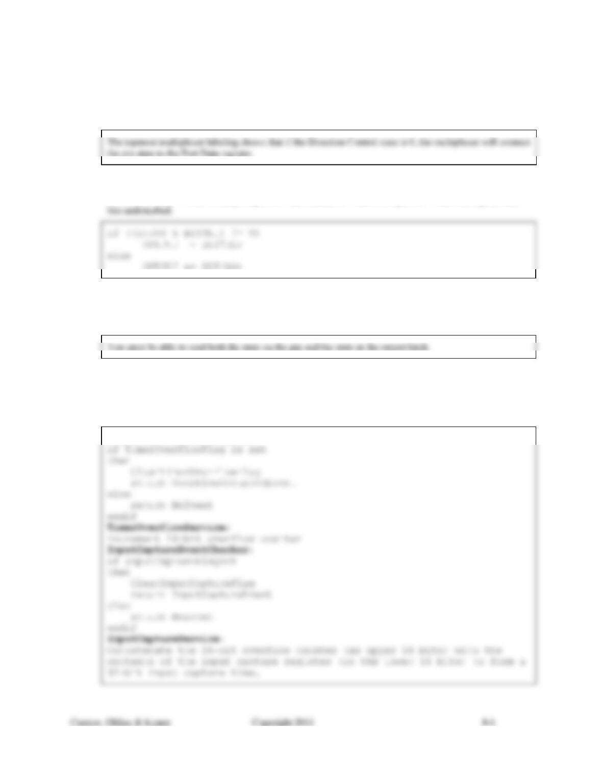
8.1) Based on the diagram of Figure 8.1, what value should you write into the DDR to make the pin an input?
8.2) Given a microcontroller that implements separate input and output registers (call them INPUT &
OUTPUT), write C code to sample input bit 3 and transfer its value to output bit 7 while leaving all other
8.3) In terms of the registers introduced in this chapter, what architecture feature is necessary to be able to tell if
an output pin is being loaded heavily enough that its output voltage is outside the input voltage range for
that state?
8.4) A particular application requires both high-resolution timing and timing of long enough intervals that the
total time can not be counted using a single 16-bit register. Write pseudo-code using other features of the
timer systems described in this chapter to implement a virtual 32-bit input capture timer. Write the pseudo-
code using an events and services paradigm (a set of event checkers and associated services).
TimerOverflowEventChecker:
8.5) Write pseudo-code for an initialization routine and an input capture event checker and service pair that
would calculate the speed of a motor assuming that the output of a 100 pulse per revolution motor was
connected to the input capture pin of a timer system being clocked by a 100 kHz clock.
InitializationRoutine:
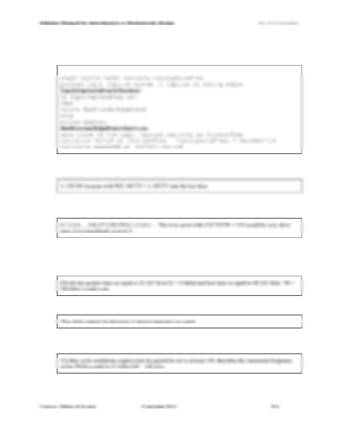
8.6) Given a PWM subsystem like shown in Figure 8.6, what duty cycle would be generated if DUTY
contained 128 and PERIOD contained 240 and POLARITY = 1?
8.7) Given a PWM subsystem like shown in Figure 8.6, with DUTY = 128 and PERIOD = 129, what sequence
of values would you expect to see in COUNTER?
8.8) Given a microcontroller with a clock rate of 24 MHz, an A/D converter clock prescaler with divide-by
ratios of 2, 4, 6, 8, 10, 12, …, 64, an A/D converter with a minimum clock speed of 500 kHz and a
maximum clock speed of 2 MHz, what range of prescale dividers result in A/D clock speeds that fall
within the A/D converter limits?
8.9) How are the Freescale DDR registers and the Microchip TRIS registers alike?
8.10) Given a PWM subsystem like that shown in Figure 8.6 with a Clock Source of 24 MHz, what is
the maximum PWM output frequency that can still achieve 1% resolution on the duty cycle?