Solution Manual for Introduction to Mechatronic Design Do Not Circulate
Chapter 10 Semiconductors
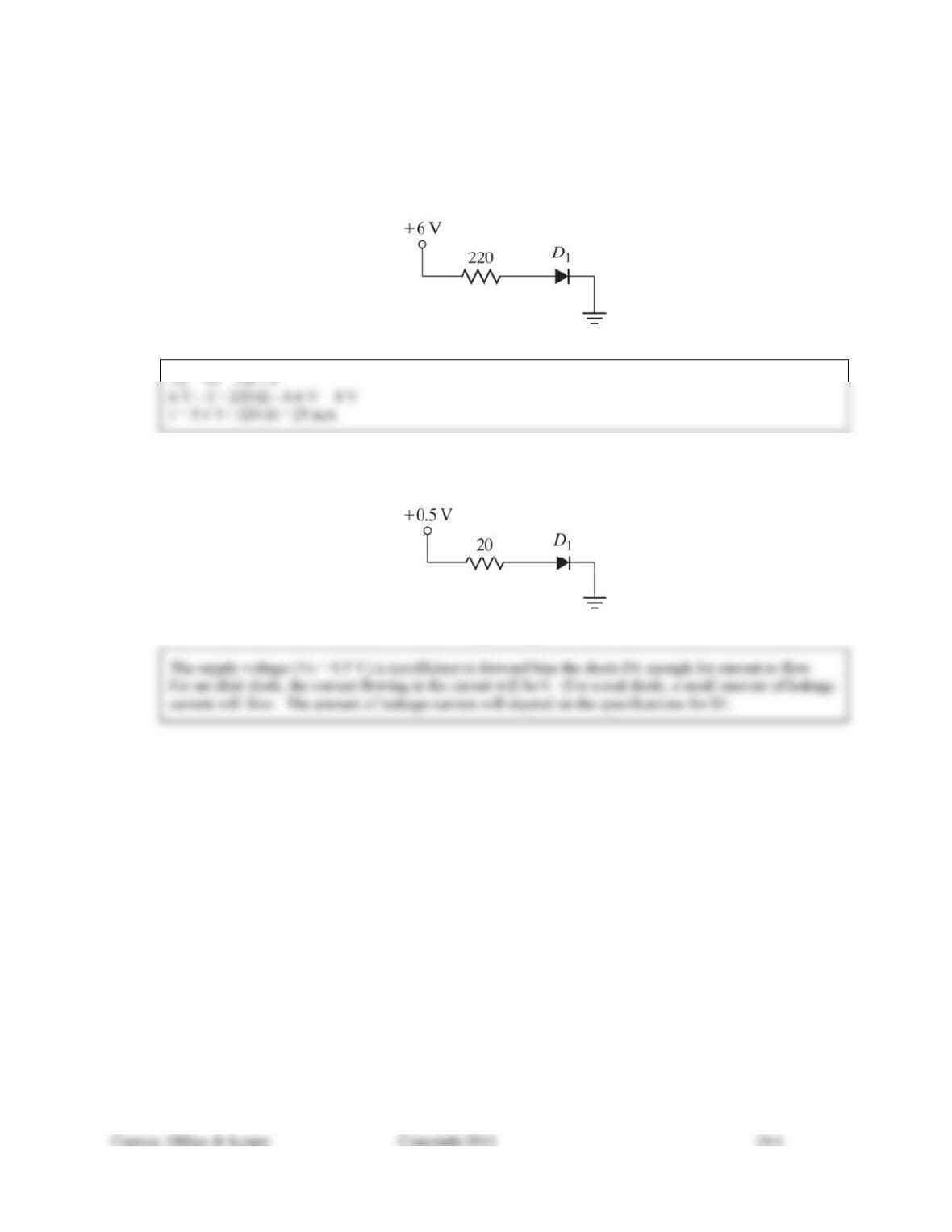
10.1) If the forward voltage drop for D1 is 0.6 V, what is the current flowing in the circuit showing in Figure
10.42? Assume that the diode behaves as an ideal diode.
Figure 10.42
10.2) If the forward voltage drop for D1 is 0.6V, what is the current flowing in the circuit in Figure 10.43?
Assume that the diode behaves as an ideal diode.
Figure 10.43
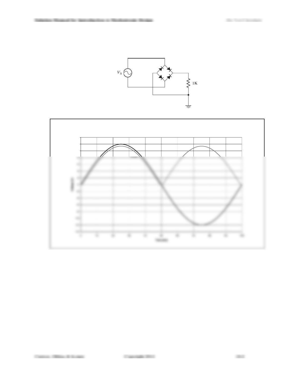
10.3) The arrangement of diodes shown in Figure 10.44 is known as a diode bridge or a full-wave rectifier.
If the output of the AC voltage source VS is 24 V peak-to-peak (±12 V) with a frequency of 100 Hz, draw a
plot of the resulting voltage drop across the resistor (assume ideal diode characteristics).
Figure 10.44
Problem 10.3 Solution
10
12
14
Vin
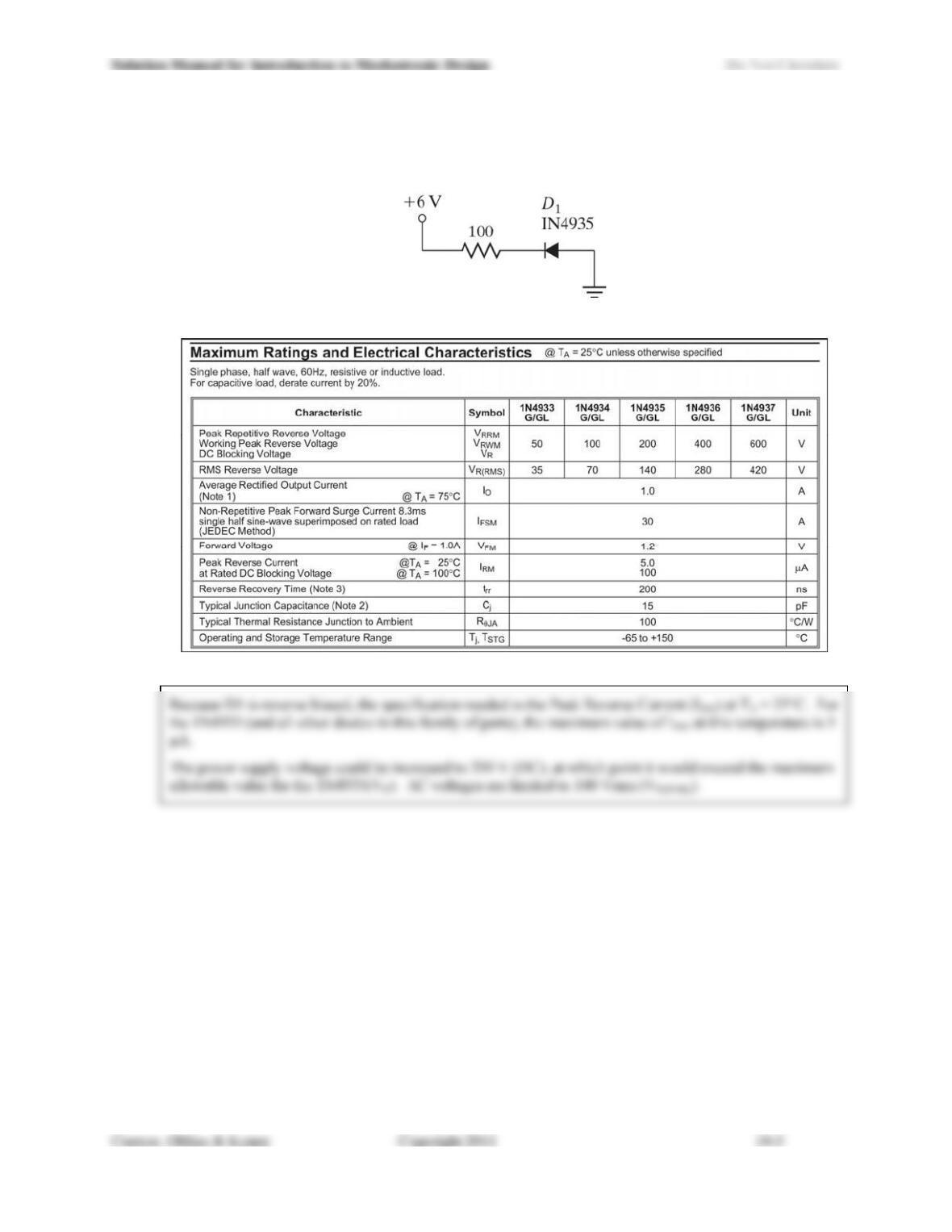
10.4) For the circuit shown in Figure 10.45, use the diode specifications provided in Figure 10.46 to determine
the maximum amount of current you can expect to flow when TA = 25°C. If you were to increase the
power supply voltage, how much could you increase it before exceeding the diodes reverse breakdown
voltage?
Figure 10.45
Figure 10.46: Data sheet excerpt. (Courtesy of Diodes Incorporated. All rights reserved.)
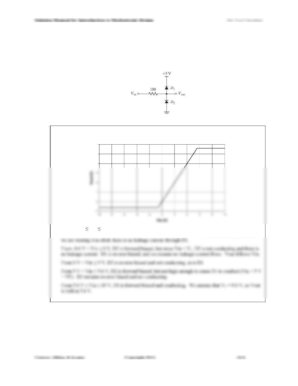
10.5) If D1 and D2 are treated as ideal diodes:
a) Draw a graph of Vout when the input voltage Vin ranges from -10 V to +10 V.
b) Draw a graph of the current flowing through the resistor over the same range of values for Vin.
c) Given that this type of circuit is commonly called a voltage clamp, briefly describe the function of
this circuit.
Figure 10.47
a)
Problem 10.5(a) Solution
4
5
6
From -10 V Vin -0.6 V, D2 is forward biased and conducting. Since we are treating D2 as ideal,
we assume that VF = 0.6 V, and this holds Vout to a value of -0.6 V. D1 is reverse biased, and since
Solution Manual for Introduction to Mechatronic Design Do Not Circulate
b)
-0.10
-0.06
-0.02
0.02
0.06
-10 -8 –6 -4 -2 0 2 4 6 8 10
Vin (V)
10.6) If the Zener voltage of the (ideal) Zener diode D1 (Figure 10.48) is 4.3 V, what is Vout when:
a) Vs = 3.3 V
b) Vs = 5 V
c) Vs = 12 V
d) Vs = -5 V
Figure 10.48
a) 3.3 V. The Zener diode is reverse biased, but not enough to cause it to go into reverse breakdown.
10.7) Design a circuit that uses a 5 V power supply to illuminate an LED that has a forward voltage drop of Vf =
2.2 V. Use only standard 5% resistors in your design, and insure that the current flowing through the LED
is between 17 and 20 mA.
+5V
R
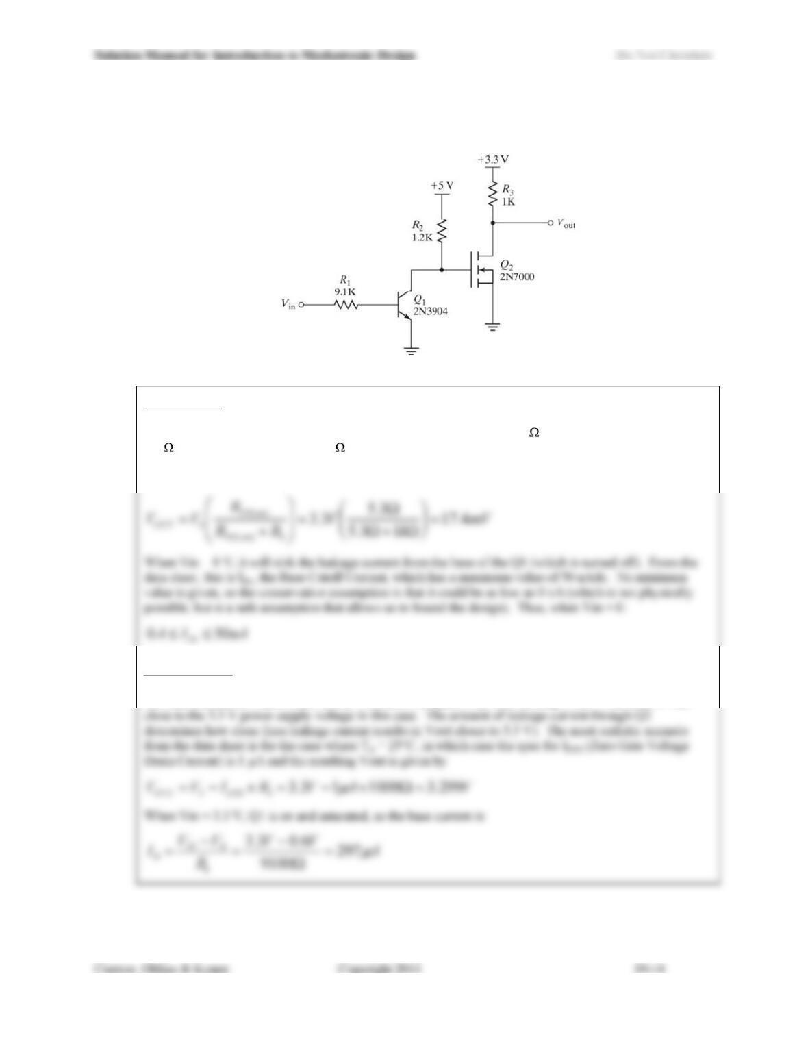
10.8) If Q2 in Figure 10.23 were replaced by an NPN transistor, what voltage would be necessary at Vin in order
to insure that Q2 is on and saturated?
The rules-of-thumb for the behavior of a typical NPN transistor tell us that it will be on and in saturation
when its base is at least 0.6 V above its emitter (VBE 0.6 V). With an NPN transistor instead of the PNP
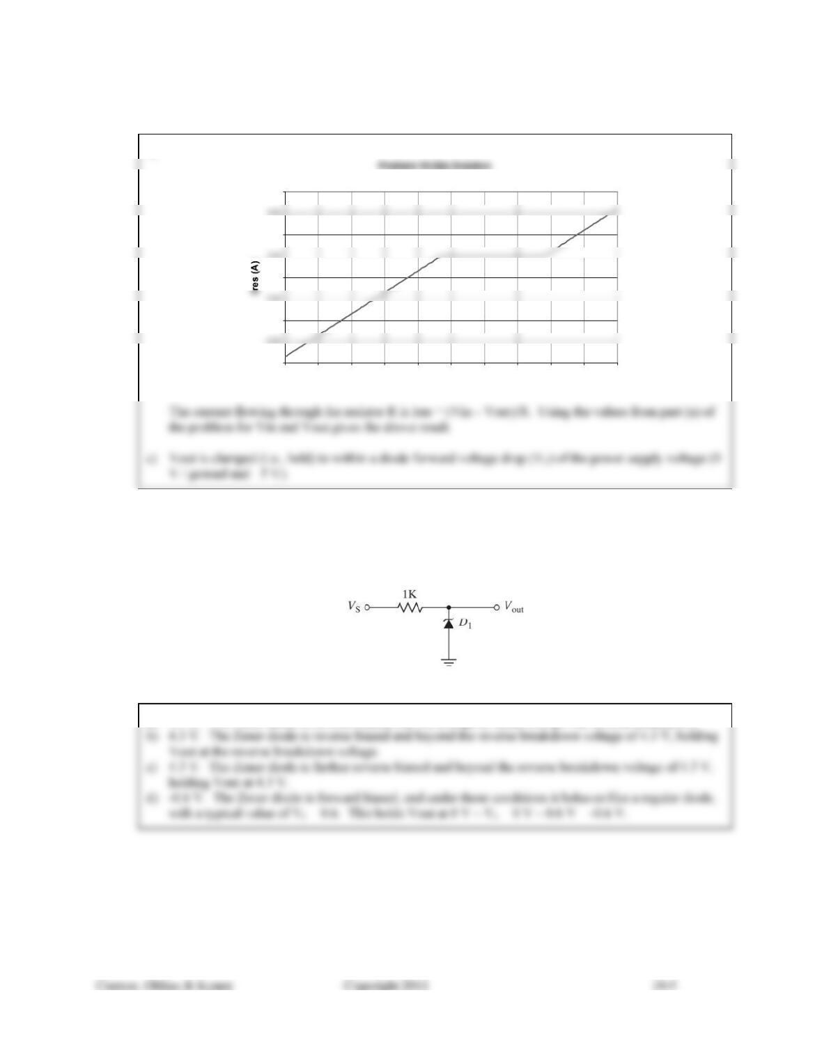
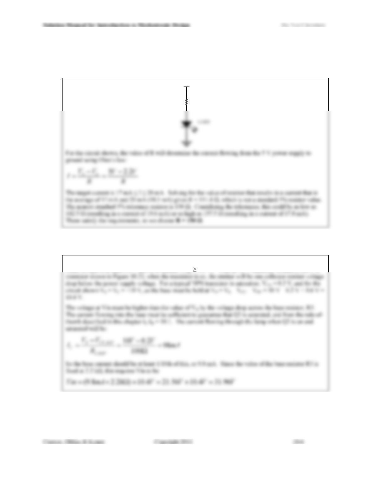
10.9) What is the minimum value of Vin required to insure that at least 2.125 A flow through the load resistor in
the circuit from Figure 10.49? Use the specifications included for the IRLZ34N N-channel MOSFET
(Figure 10.50). What is the power dissipated in the resistor under these conditions? In the MOSFET?
Figure 10.49
Figure 10.50
In order for the specified current to flow through the load, the RDS(on) for Q1 is determined from:
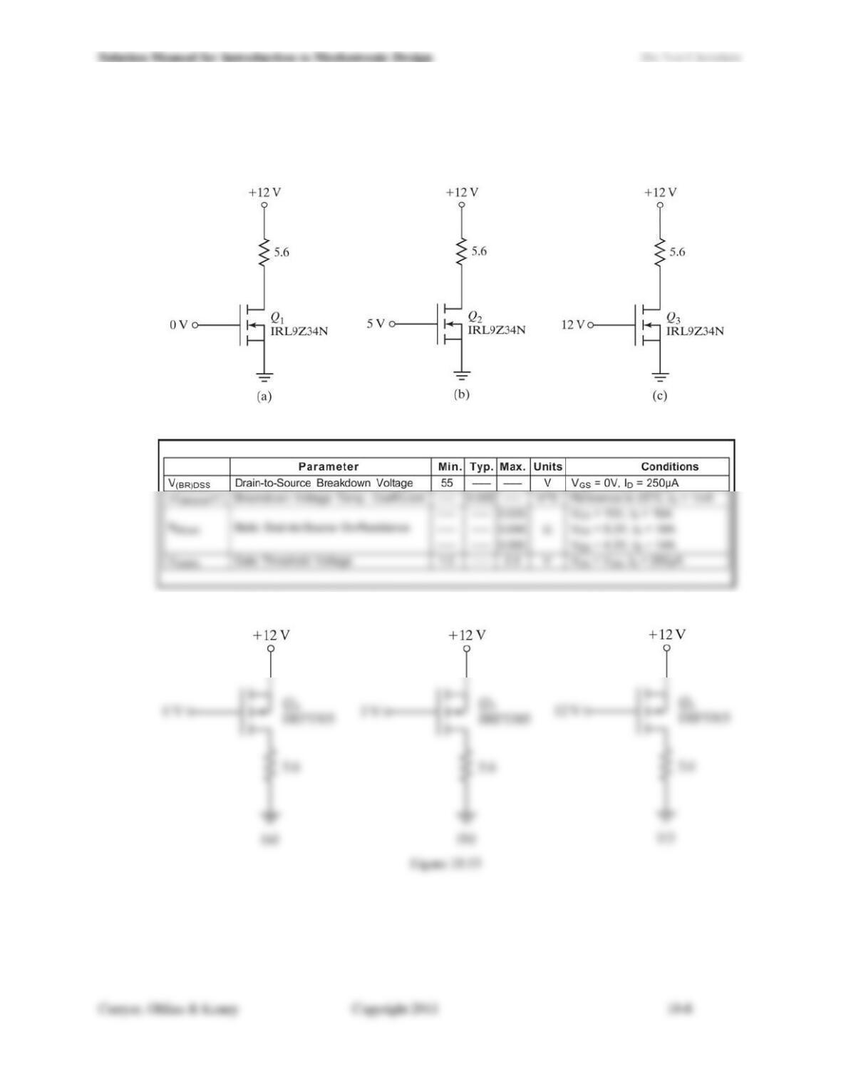
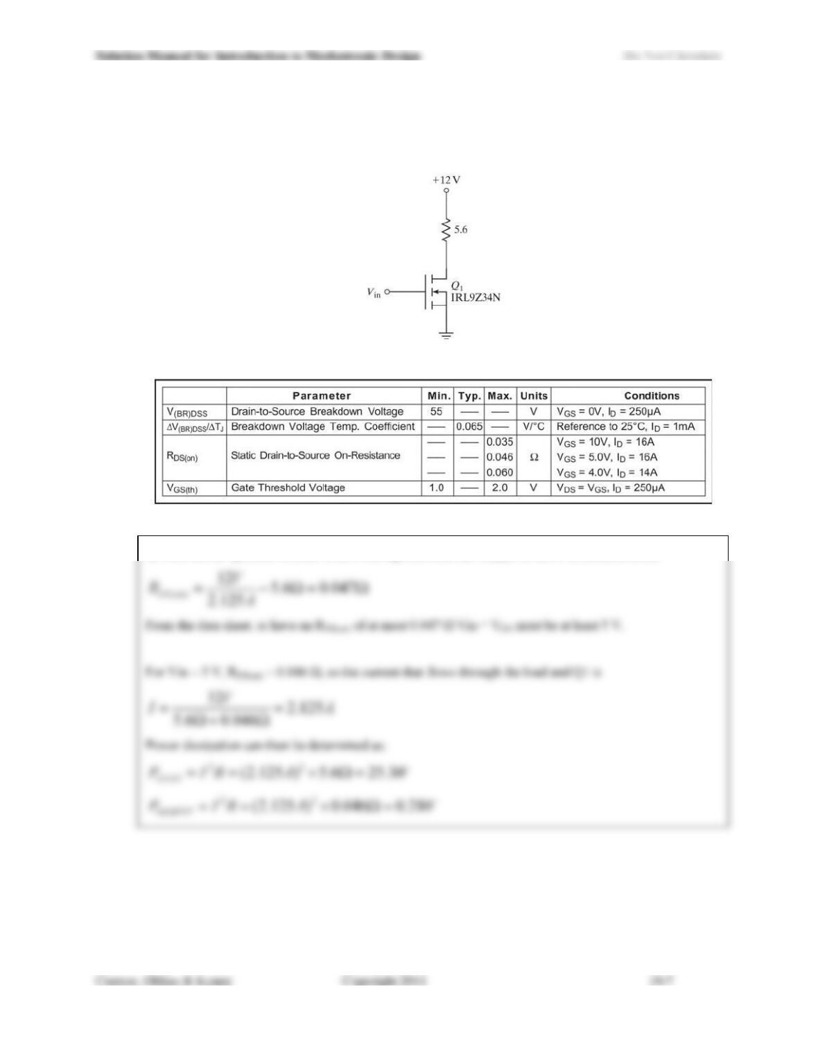
10.10) For each of the following circuits from Figures 10.51 and 10.53, state whether the transistor is off, on but
not operating in the linear region, or on and operating in the linear region. Where possible, calculate the
minimum current that will flow through the load resistor using the specifications given in Figures 10.52
and 10.54.
Figure 10.51
Figure 10.52: IRL9Z34N data sheet excerpt. (Courtesy of International Rectifier © 1998.)
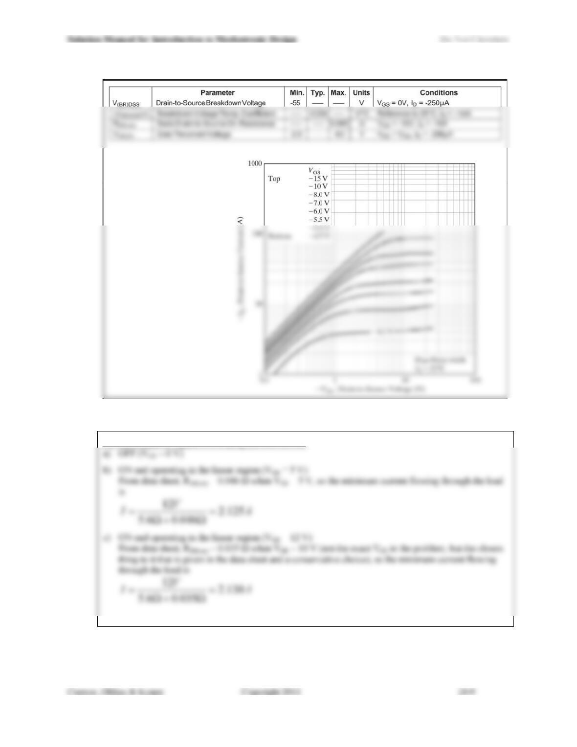
Figure 10.54: IRFU5305 data sheet excerpt. (Courtesy of International Rectifier © 2000.)
For the circuits in Figure 10.51, using the IRL9Z34N:
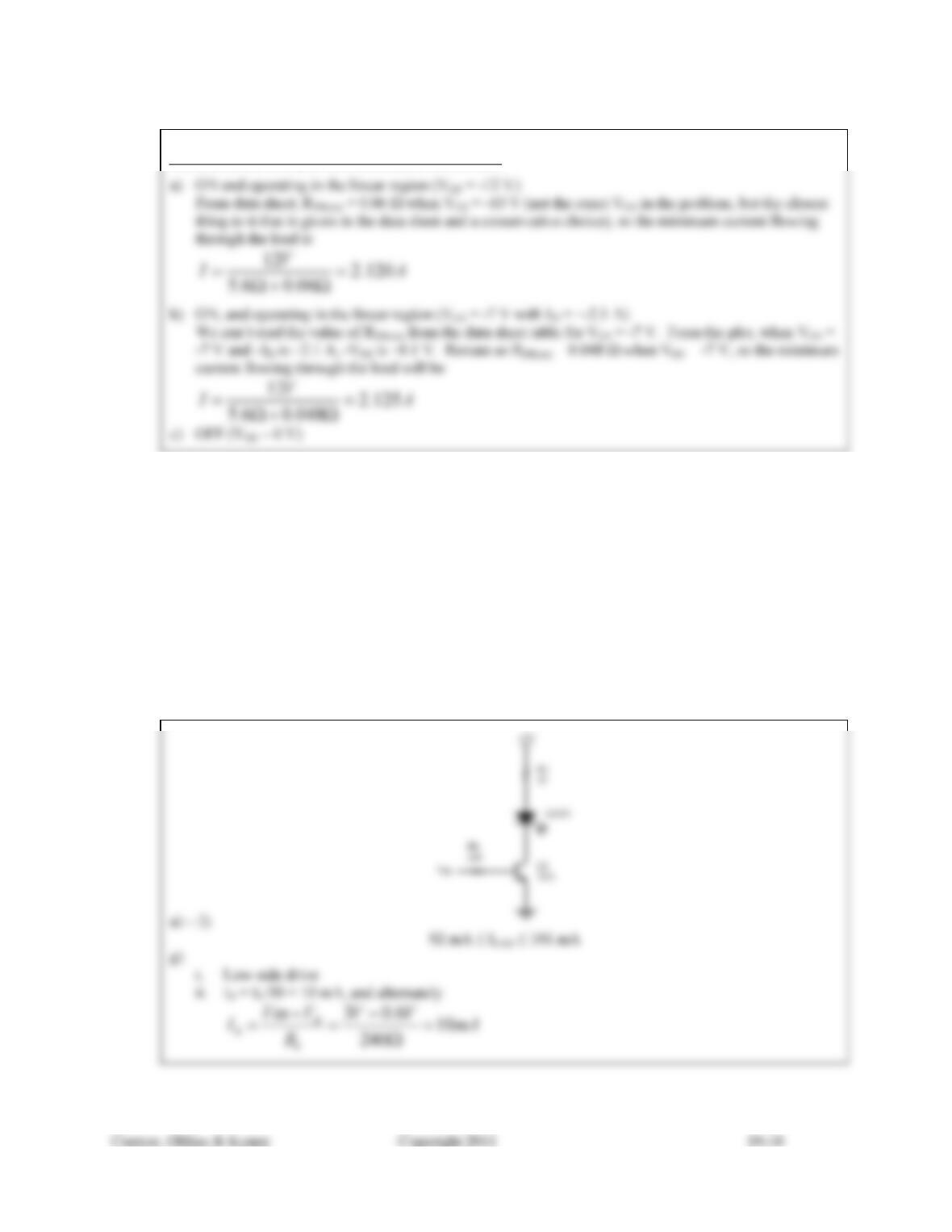
Solution Manual for Introduction to Mechatronic Design Do Not Circulate
For the circuits in Figure 10.53, using the IRFU5305:
10.11) Design a circuit that satisfies all of the following conditions:
a) Use a single BJT (use rule-of-thumb characteristics for the BJT, and insure operation in the saturated
region).
b) Use the BJT to switch the current flowing through an LED (Vf = 2.2 V).
c) Use a 5 V power supply.
d) The base of the BJT is driven by a signal that is 0 V when the LED is to be off and 3 V when the LED
is to be on.
e) The current through the LED is approximately 0 mA in the off state and 100 mA (± 10%) in the on
state.
f) Use standard 5% resistor values.
g) Answer the following:
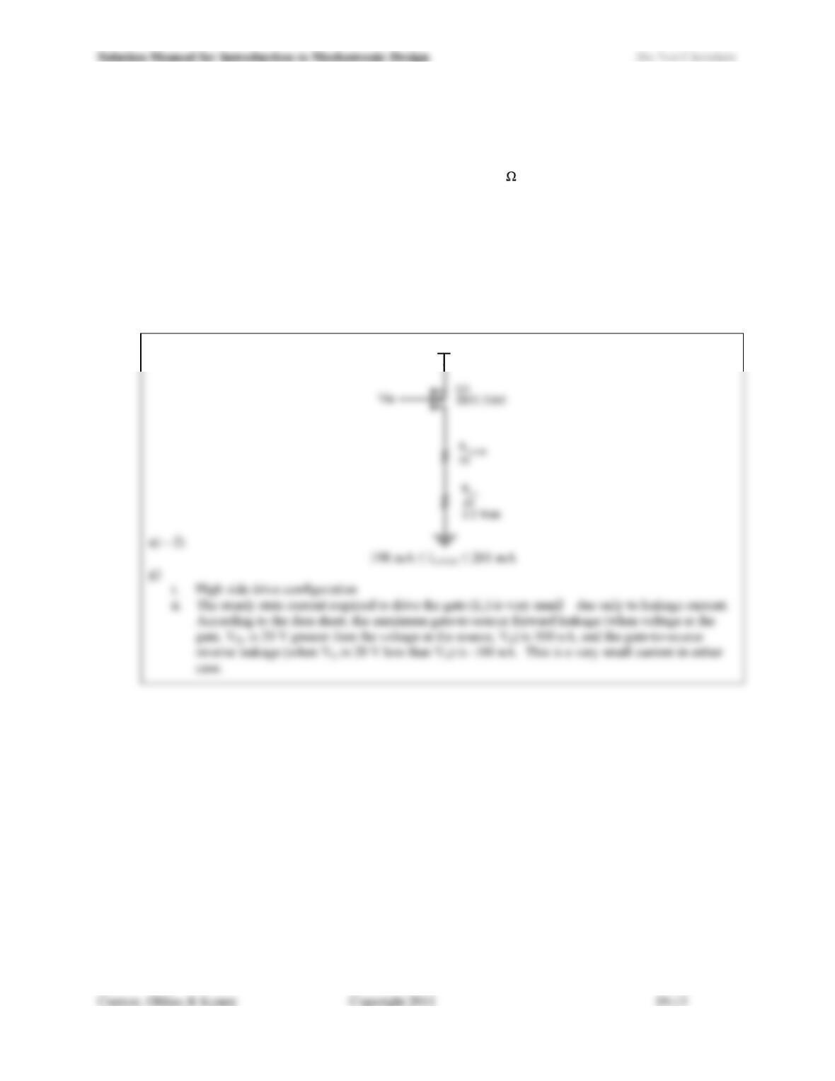
i. Is this a low-side drive or a high-side drive configuration?
ii. How much steady-state current is required to drive the base of the BJT?
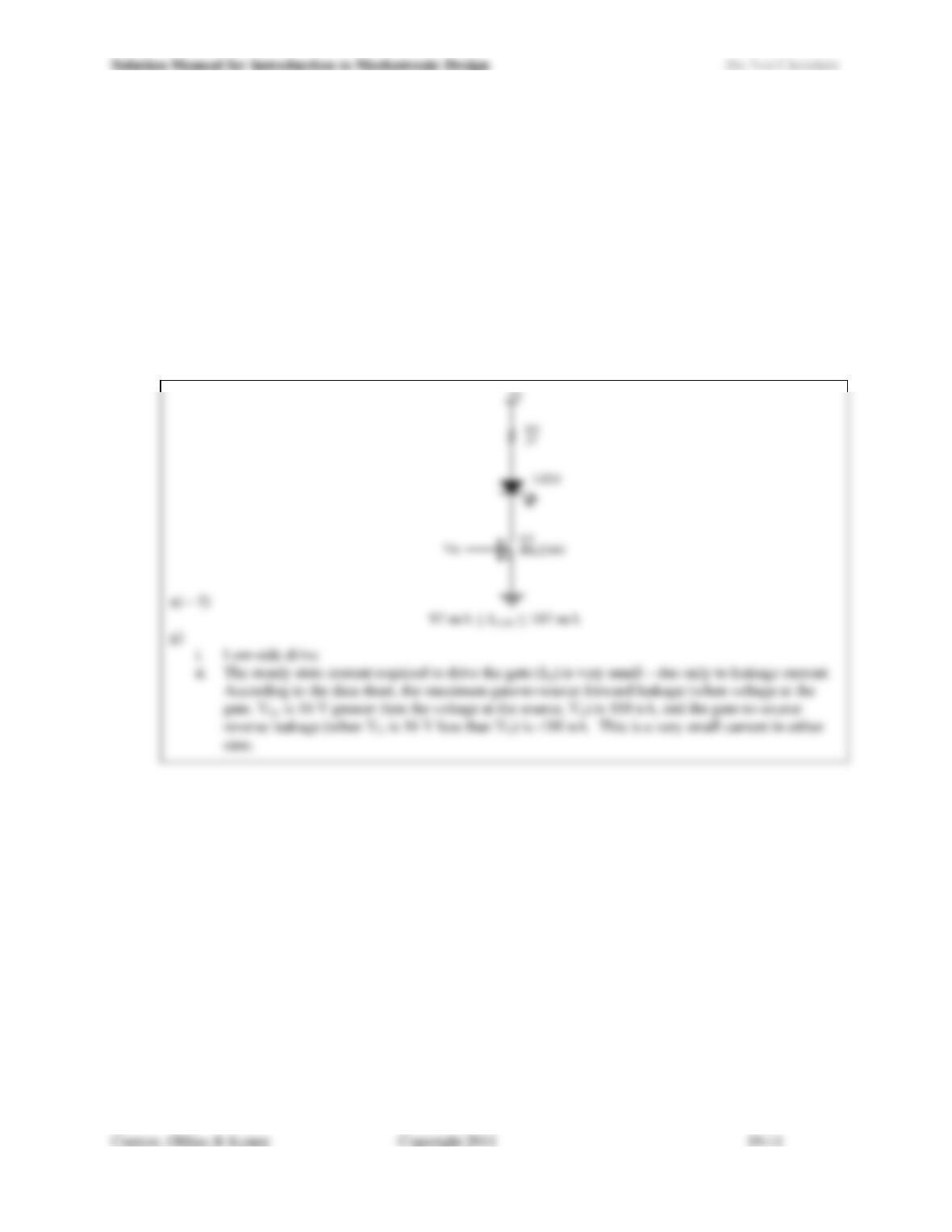
10.12) Design a circuit that satisfies all of the following conditions:
a) Use a single IRL9Z34N N-channel MOSFET (the data sheet for this component may be found on the
Internet). Operate the MOSFET in the linear region.
b) Use the MOSFET to switch the current flowing through and LED (Vf = 2.2 V).
c) Use a 5 V power supply.
d) The gate of the IRL9Z34N is driven by a signal that is 0 V when the LED is to be off and 5 V when the
LED is to be on.
e) The current through the LED is approximately 0 mA in the off state and 100 mA (± 10%) in the on
state.
f) Use standard 5% resistor values.
g) Answer the following:
i. Is this a low-side drive or a high-side drive configuration?
ii. How much steady-state current is required to drive the gate of the IRL9Z34N?
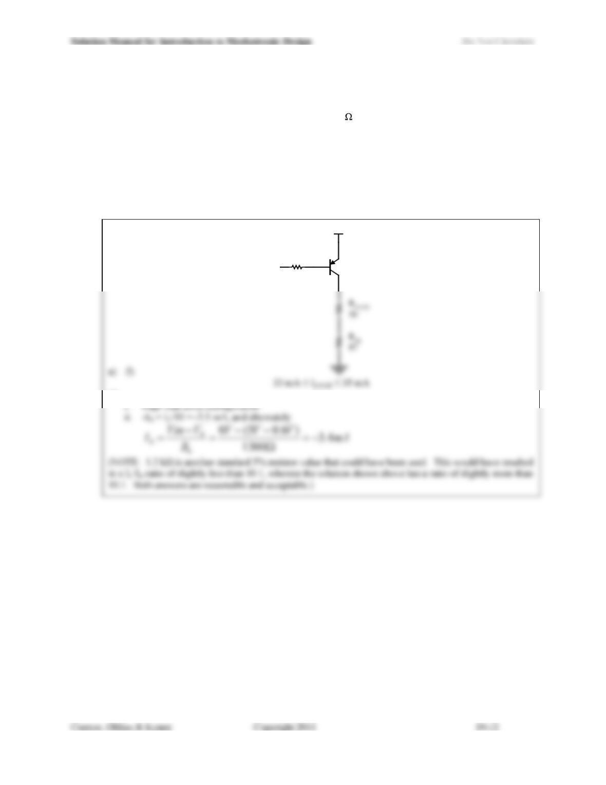
10.13) Design a circuit that satisfies all of the following conditions:
a. Use a single BJT (assume ideal characteristics, and operate the BJT in the saturated region).
b. Use the BJT to switch the current flowing through a 50 load.
c. Use a 5 V power supply.
d. The base of the BJT is driven by a signal that is 5 V when the load is to be off and 0 V when the load is
to be on.
e. The current through the load is approximately 0 mA in the off state and 35 mA (± 10%) in the on state.
f. Use standard 5% resistor values.
g. Answer the following:
i. Is this a low-side drive or a high-side drive configuration?
ii. How much steady-state current is required to drive the base of the BJT?
+5V
1.3K
Rb
Vin PNP BJT
Q1
g)
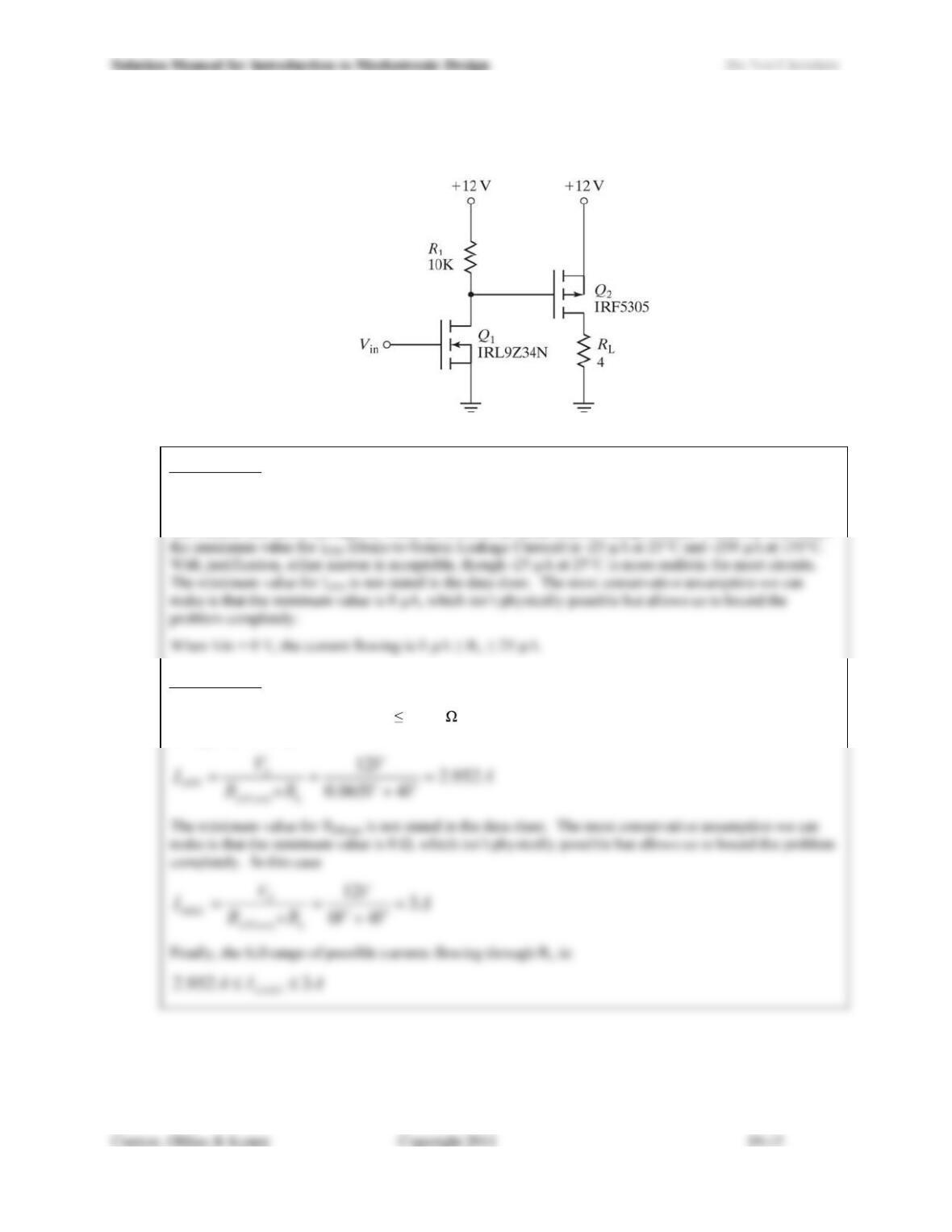
10.14) Design a circuit that satisfies all of the following conditions:
a. Use a single IRFU5305 P-channel MOSFET (the data sheet for this component may be found on the
Internet). Operate the MOSFET in the linear region.
b. Use the MOSFET to switch the current flowing through a 50 load.
c. Use a 12 V power supply.
d. The base of the BJT is driven by a signal that is 12 V when the load is to be off and 0 V when the load
is to be on.
e. The current through the load is approximately 0 mA in the off state and 200 mA (± 10%) in the on
state.
f. Use standard 5% resistor values.
g. Answer the following:
i. Is this a low-side drive or a high-side drive configuration?
ii. How much steady-state current is required to drive the gate of the IRFU5305?
+12V
10.15) For the circuit shown in Figure 10.55, what is the voltage at Vout when Vin = 0 V? What is Vout when
Vin = 3.3 V? How much current will Vin be required to source or sink in each state?
Figure 10.55
For Vin = 0 V:
Q1 is off and the gate of Q2 is pulled high to 5 V through R2. This turns Q2 on and it operates in the linear
region. The data sheet for the 2N7000 states that RDS(ON) is typically 1.8 and has a maximum value of
5.3 . Assuming that RDS(ON) = 5.3 represents the worst case design (the problem statement doesnt
specify, but typically the goal is to get Vout as close to 0 V in this state as possible), we will determine
Vout for this condition:
For Vin = 3.3 V:
Q1 is on and saturated (IC/IB = 13.5, which is slightly more than the rule-of-thumb goal of 10, but much
less than the rule-of-thumb limit of 20). This pulls the gate of Q2 low, turning it off. Vout will be very
10.16) What is the current that flows through RL when Vin = 0 V? What is the current through RL when Vin = 5
V? How much current will Vin be required to source or sink in each state? Refer to Figure 10.56.
Figure 10.56
For Vin = 0 V:
Q1 is off, and the gate of Q2 is pulled to 12 V through R1. Since Q2 is a P-channel MOSFET, this turns it
off.
The current that flows through RL when Q2 is off is the drain-source leakage current. From the data sheet,
For Vin = 5 V:
Q1 is on and operating in the linear region, which will pull Q2s gate near 0 V, turning Q2 on. From the
datasheet for the IRFU5305, RDS(on) 0.065 when VGS = -10 V. Thus, the minimum current flow
through RL when Q2 is on will be: