Problems 15–41
[b] G2=1
2(1 + 4) =0.1 S;
[c] kf=ω0
o
ωo
=2π(2500) = 5000π;
km=C2
C0
2kf
=1
(10 ⇥109)kf
= 6366.2;
;
[d] R0
1=R0
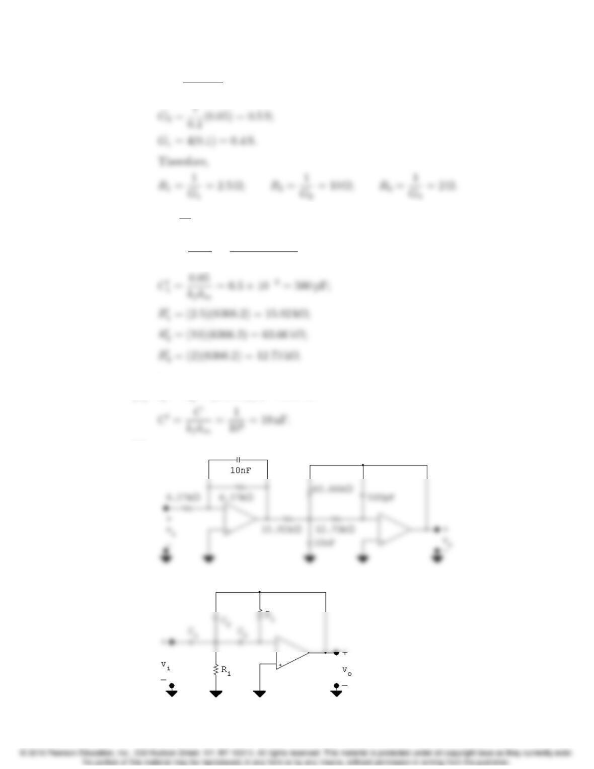
2= (6366.2)(1) = 6.37 kΩ
[e]
P 15.50 [a] By hypothesis the circuit becomes:
15–42 CHAPTER 15. Active Filter Circuits
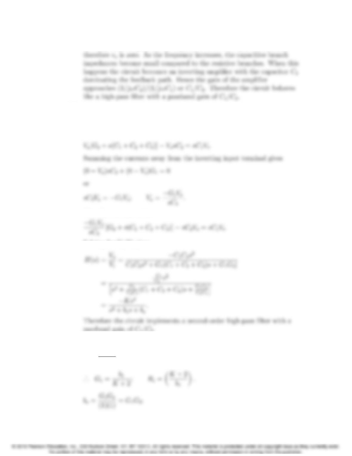
For very small frequencies the capacitors behave as open circuits and
[b] Summing the currents away from the upper terminal of R2yields
VaG2+(VaVi)sC1+(VaVo)sC2+VasC3=0
or
Therefore we can write
Solving for Vo/Vigives
[c] C1=K:
b1=G1
(1)(1)(K+2)=G1(K+ 2);
Problems 15–43
[d] From Table 15.1 the transfer function of the second-order section of a
third-order high-pass Butterworth filter is
Thus
C1=K= 8 F;
P 15.51 [a] Low-pass filter:
choose C1=0.03 F;
15–44 CHAPTER 15. Active Filter Circuits
In the second second-order prototype circuit:
Arbitrarily select the larger value, then
G2=0.7139 S; ·
.. R
2=1
G2
=1.4008 Ω;
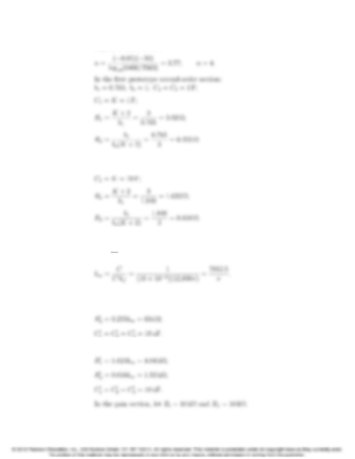
In the low-pass section of the filter
kf=ω0
o
ωo
=2π(400) = 800π;
Therefore in the first scaled second-order section
R0
1=R0
2=2.96km= 118 kΩ;
In the second scaled second-order section
R0
1=R0
2=1.4008km= 55.74 kΩ;
Problems 15–45
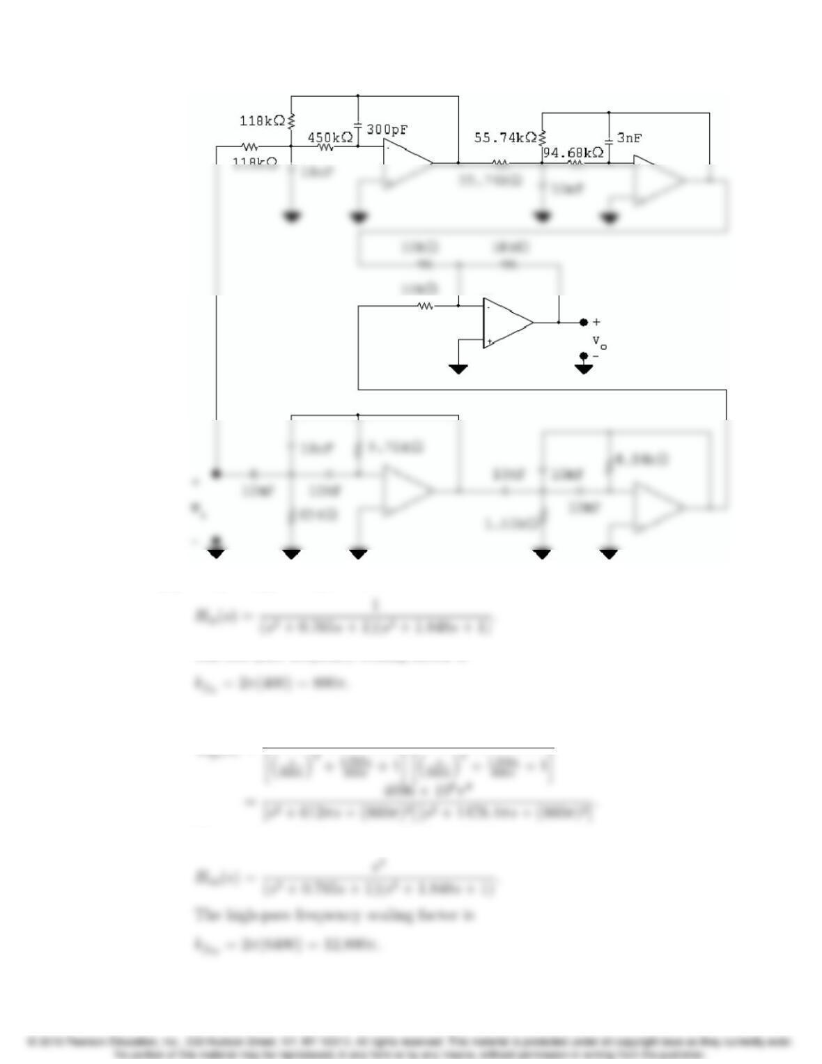
High-pass filter section
In the second prototype second-order section: b1=1.848; bo= 1;
C2=C3= 1 F;
In the high-pass section of the filter
kf=ω0
o
ωo
=2π(6400) = 12,800π;
In the first scaled second-order section
R0
1=3.92km=9.75 kΩ;
1=C0
2=C0
3= 10 nF.
In the second scaled second-order section
15–46 CHAPTER 15. Active Filter Circuits
[b]
P 15.52 [a] The prototype low-pass transfer function is
The low-pass frequency scaling factor is
The scaled transfer function for the low-pass filter is
H0
⇣s
⇣s
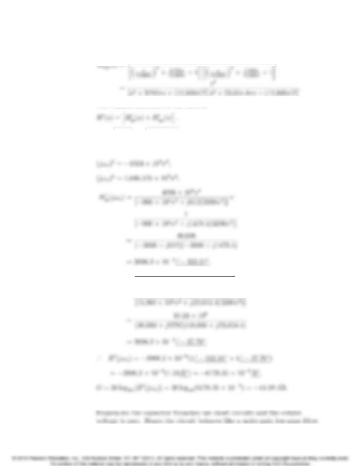
The prototype high-pass transfer function is
Problems 15–47
The scaled transfer function for the high-pass filter is
The transfer function for the filter is
[b] fo=qfc1fc2=q400)(6400) = 1600 Hz;
ωo=2πfo= 3200πrad/s;
H0
hp(jωo)= 1,048,576 ⇥108π4
[15,360 ⇥104π2+j9792(3200π2)]
1
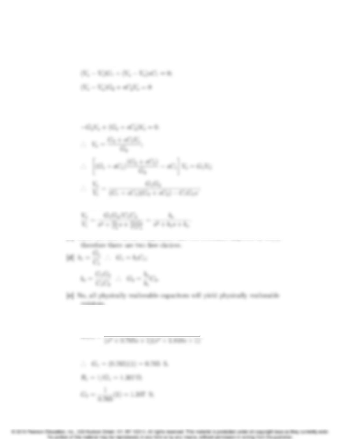
P 15.53 [a] At low frequencies the capacitor branches are open; vo=vi. At high
15–48 CHAPTER 15. Active Filter Circuits
[b] Let varepresent the voltage-to-ground at the right-hand terminal of R1.
Observe this will also be the voltage at the left-hand terminal of R2. The
s-domain equations are
or
(G1+sC1)VasC1Vo=G1Vi
which reduces to
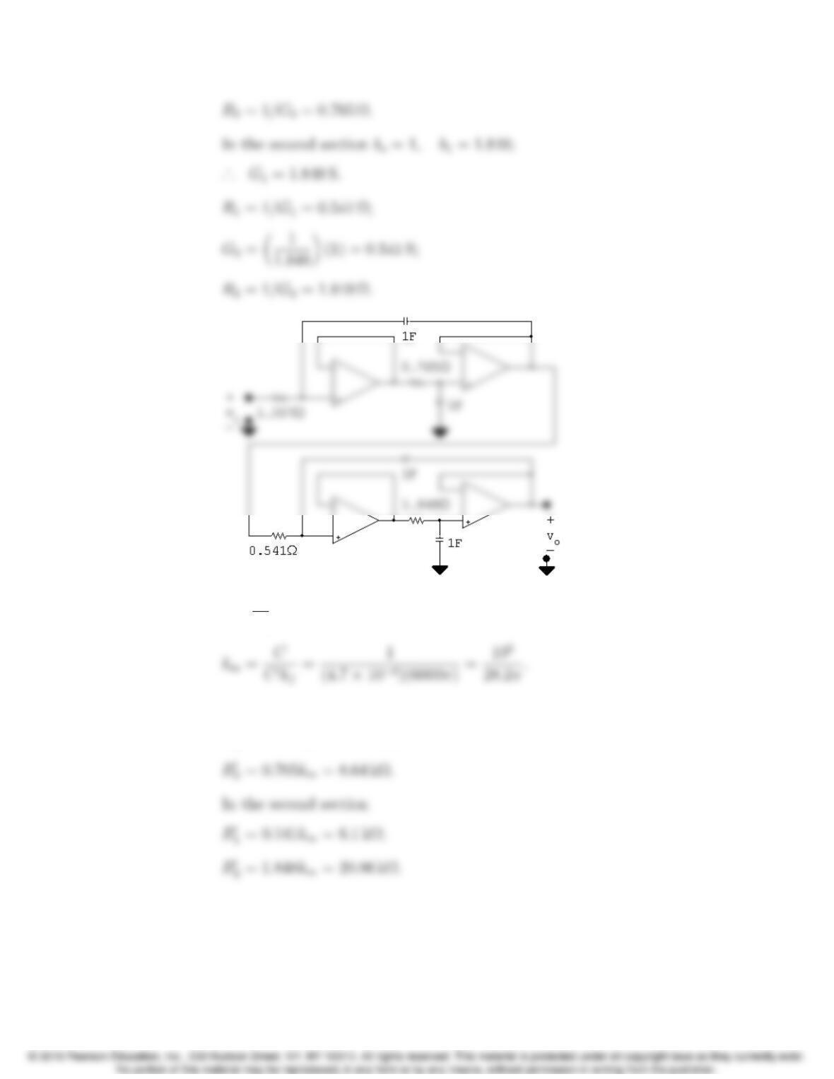
[c] There are four circuit components and two restraints imposed by H(s);
resistors.
[f] From Table 15.1 we know the transfer function of the prototype 4th order
Butterworth filter is
In the first section bo=1,b
1=0.765;
Problems 15–49
P 15.54 [a] kf=ω0
o
ωo
=2π(3000) = 6000π;
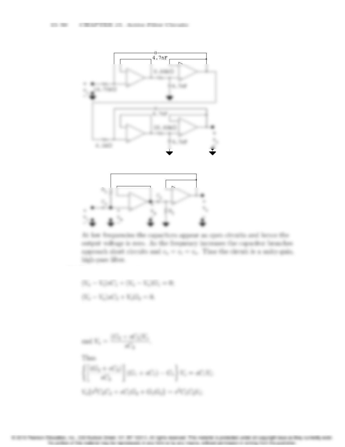
In the first section
R0
1=1.307km= 14.75 kΩ;
[b]
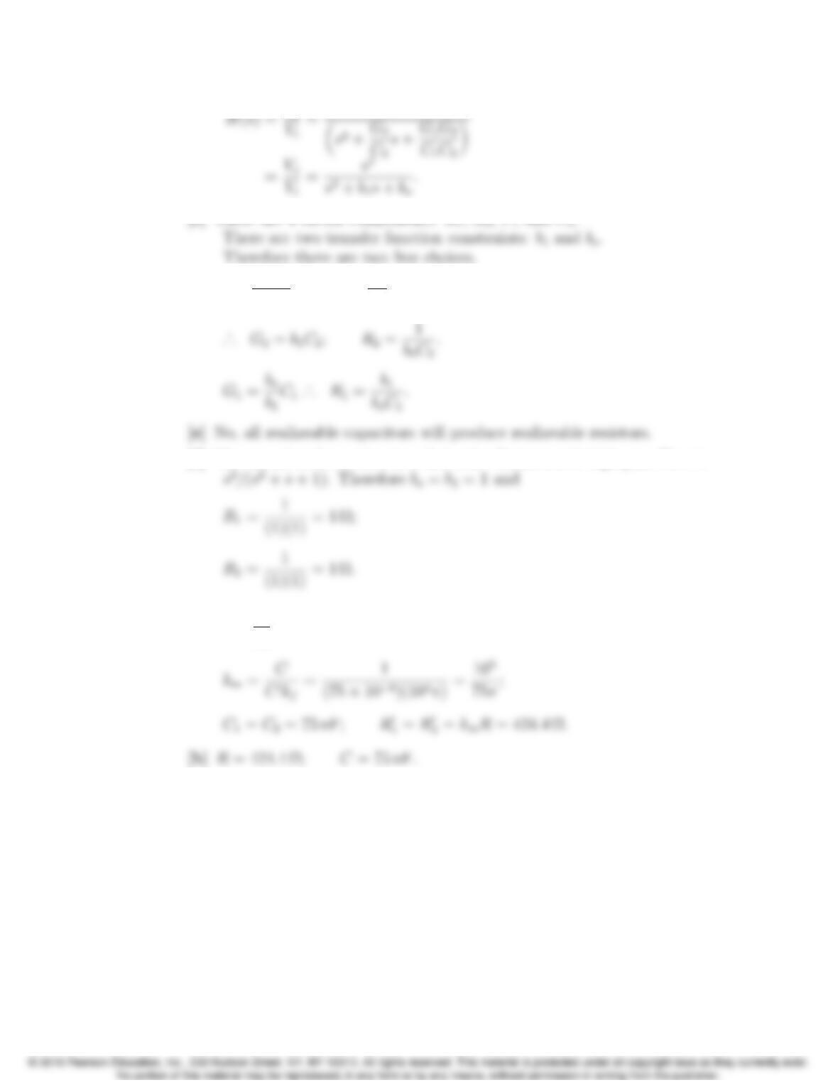
P 15.55 [a] Interchanging the Rs and Cs yields the following circuit.
[b] The s-domain equations are
It follows that
Va(G1+sC1)G1Vo=sC1Vi
Problems 15–51
[c] There are 4 circuit components: R1,R2,C1and C2.
[d] bo=G1G2
C1C2
;b1=G2
C2
;
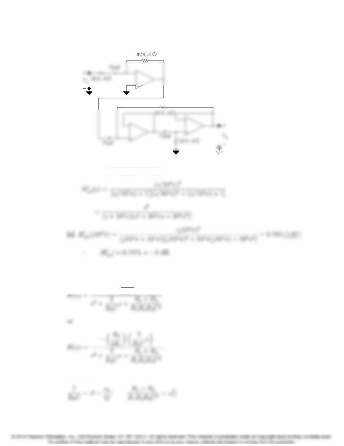
[f] The second-order section in a 3rd-order Butterworth high-pass filter is
P 15.56 [a] kf=ω0
o
ωo
= 104π;
15–52 CHAPTER 15. Active Filter Circuits
[c]
[d] Hhp(s)= s3
(s+ 1)(s2+s+1);
P 15.57 From Eq 15.19 we can write
✓1
R1C◆s
Therefore
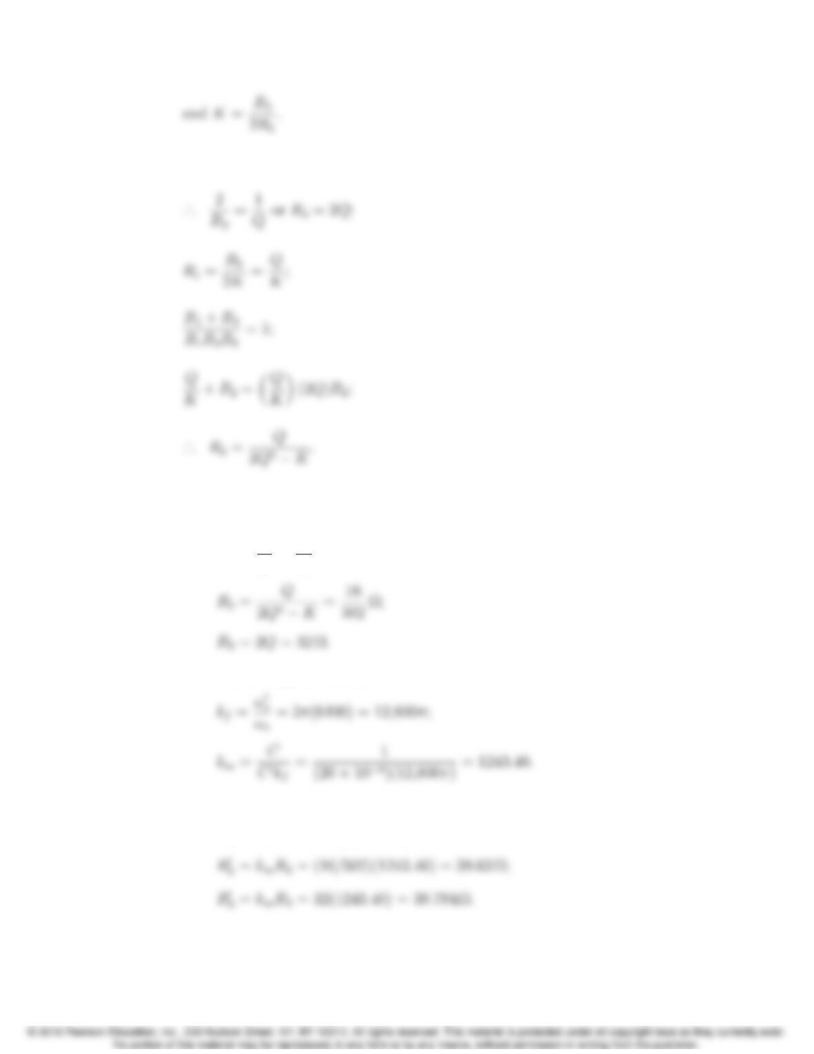
Problems 15–53
By hypothesis C= 1 F and ωo= 1 rad/s;
P 15.58 [a] From the statement of the problem, K= 10 ( = 20 dB). Therefore for the
prototype bandpass circuit
R1=Q
K=16
10 =1.6Ω;
The scaling factors are
Therefore,
R0
1=kmR1= (1.6)(1243.30) = 1.99 kΩ;
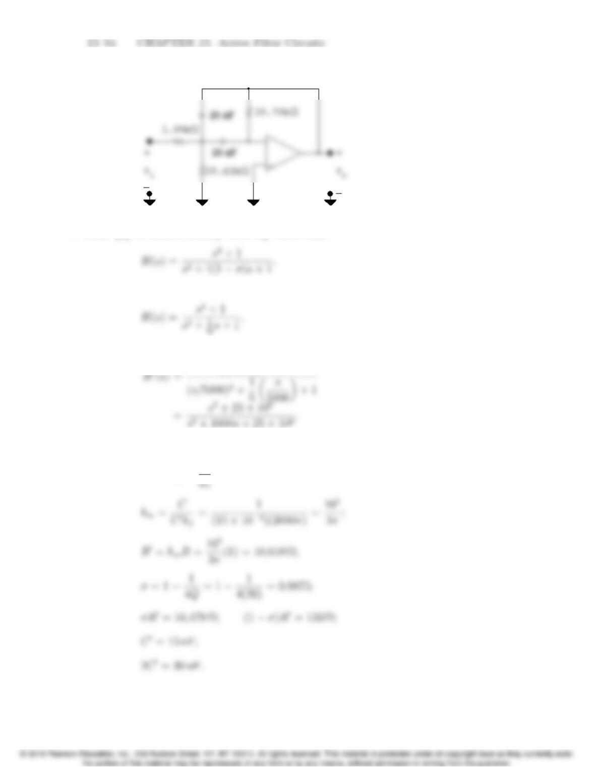
[b]
P 15.59 [a] It follows directly from Eq. 15.21 that
Now note from Eq 15.22 that (1 σ) equals 1/4Q, hence
[b] For Example 15.14 ωo= 5000 rad/s and Q= 5. Therefore kf= 5000 and
P 15.60 [a] ωo= 2000πrad/s;
·
.. k
f=ω0
o
= 2000π;
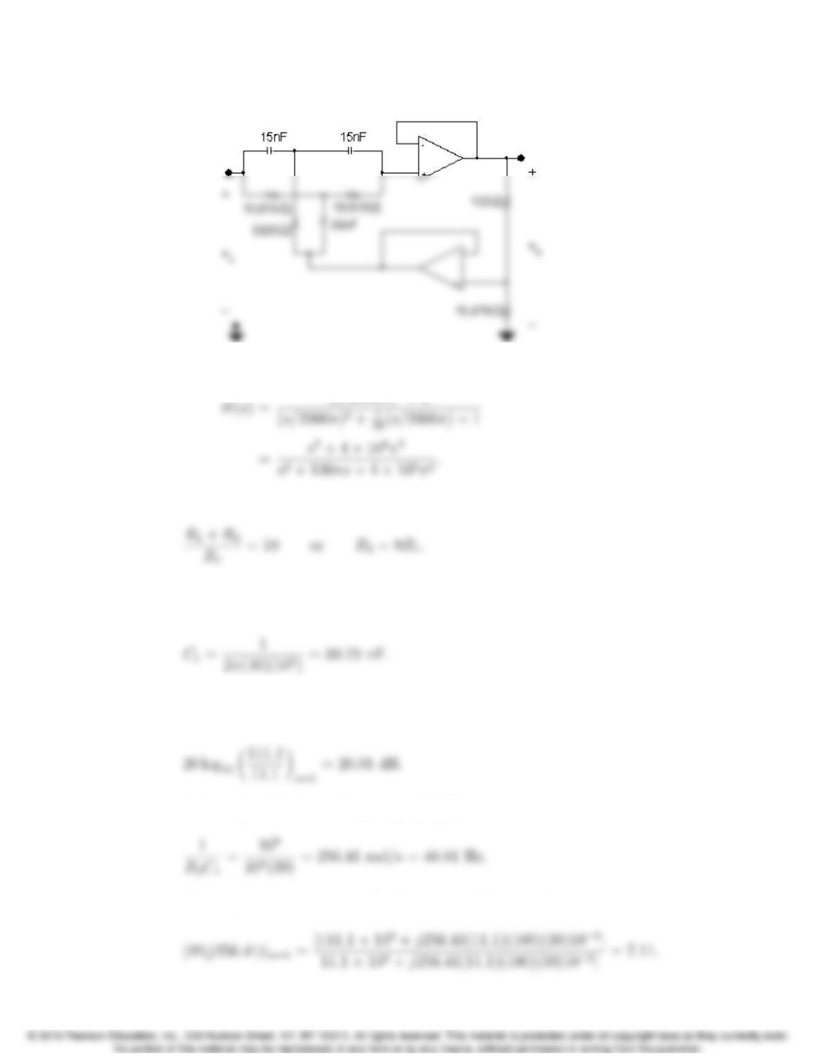
Problems 15–55
[b]
[c] kf= 2000π;
P 15.61 To satisfy the gain specification of 20 dB at ω= 0 and α= 1 requires
Choose a standard resistor of 11.1 kΩfor R1and a 100 kΩpotentiometer for
R2. Since (R1+R2)/R11 the value of C1is
Choose a standard capacitor value of 39 nF. Using the selected values of R1
and R2the maximum gain for α= 1 is
When C1= 39 nF the frequency 1/R2C1is
The magnitude of the transfer function at 256.41 rad/s is
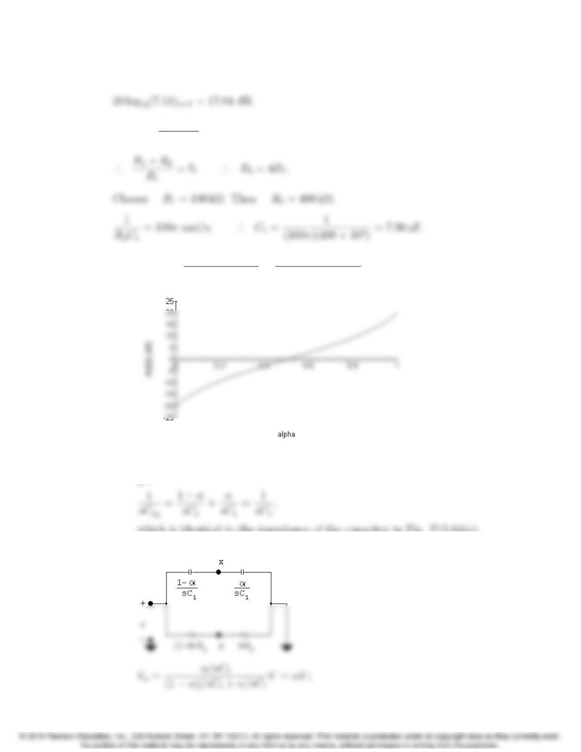
15–56 CHAPTER 15. Active Filter Circuits
Therefore the gain at 40.81 Hz is
P 15.62 20 log10 ✓R1+R2
R1◆= 13.98;
P 15.63 [a] |H(j0)|=R1+αR2
R1+ (1 α)R2
=11.1+α(100)
11.1+(1α)100.
P 15.64 [a] Combine the impedances of the capacitors in series in Fig. P15.64(b) to
get
which is identical to the impedance of the capacitor in Fig. P15.64(a).
[b]
Problems 15–57
[d] The feedback path between Voand Vscontaining the resistance R4+2R3
has no effect on the ratio Vo/Vs, as this feedback path is not involved in
the nodal equation that defines the voltage ratio. Thus, the circuit in
P 15.65 As ω!0
|H(jω)|!2R3+R4
2R3+R4
=1.
Therefore the circuit would have no effect on low frequency signals. As ω!1
15–58 CHAPTER 15. Active Filter Circuits
If R4Ro
Thus, the transition from amplification to attenuation occurs at β=0.5. If
β>0.5 we have amplification, and if β<0.5 we have attenuation.
Also note the amplification an attenuation are symmetric about β=0.5. i.e.
P 15.66 [a] |H(j1)|β=1 =Ro(R4+R3)
R3(R4+Ro)=(65.9)(505.9)
(5.9)(565.9) =9.99;
[d] |H(j/R3C2)|β=1 =
(2R3+R4)+jRo
R3(R4+R3)
(2R3+R4)+j(R4+Ro)
Problems 15–59
[e] When β=0
maximum.
P 15.67 |H(j1)|=[(1 β)R4+Ro][βR4+R3]
[(1 βR4+R3][βR4+Ro]