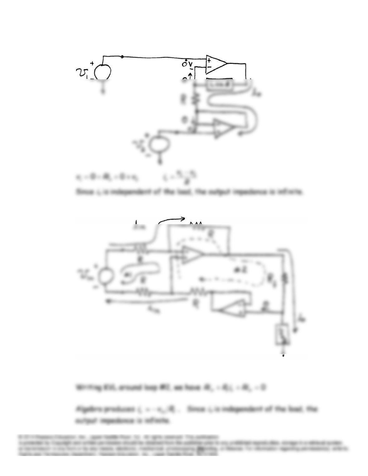
P14.25 (a)
(b) The circuit diagram is:
Writing KVL around loop #1, we have
ininin RiRiv
0
P14.26 (a) Using the summing-point constraint, KCL, KVL, and Ohm’s law, we find
the currents:
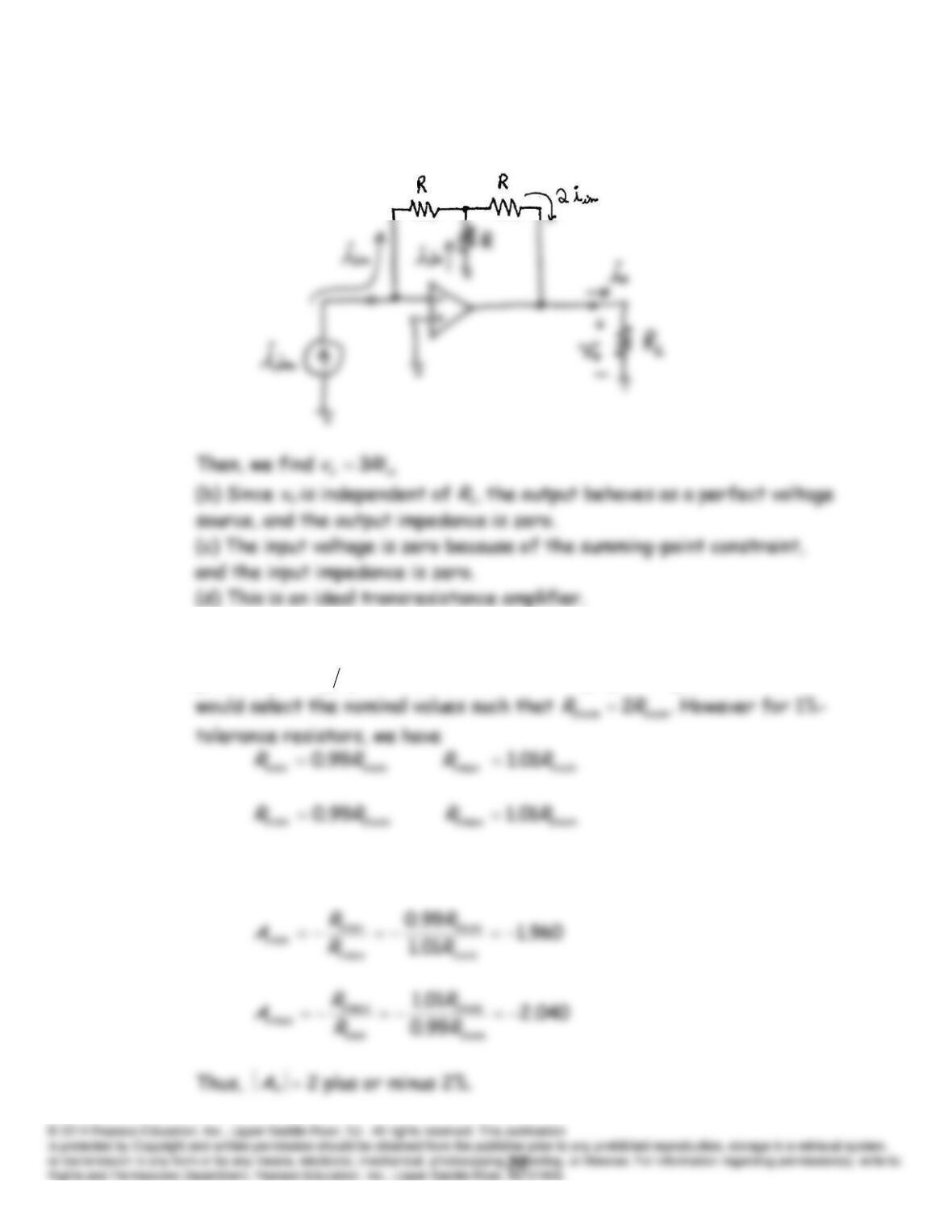
P14.27 The inverting amplifier is shown in Figure 14.4 in the text and the voltage
gain is
12
RRAv
. Thus, to achieve a voltage gain magnitude of 2, we
Thus we have
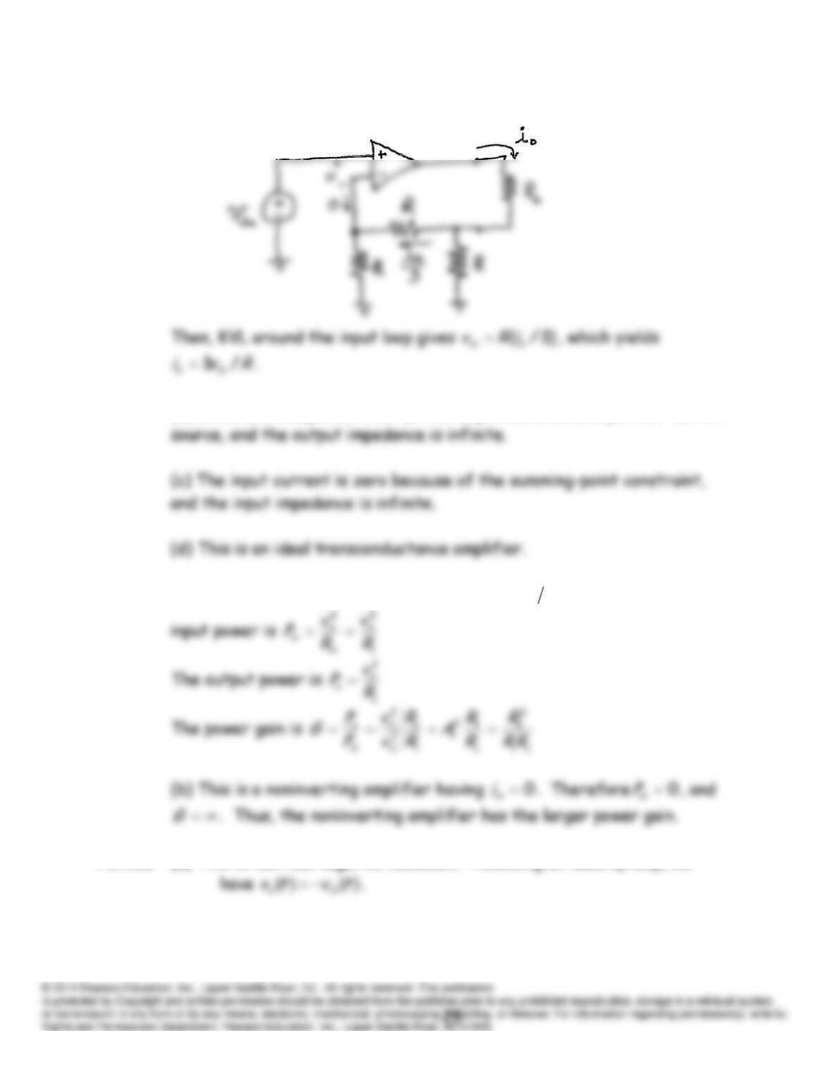
P14.28 (a) Using the current-division principle, we find the currents as shown:
(b) Since
io
is independent of
RL
, the output behaves as a perfect current
P14.29 (a) This is an inverting amplifier having
12
RRAv
and
1
RRin
. The
P14.30* (a) This circuit has negative feedback. Assuming an ideal op amp, we
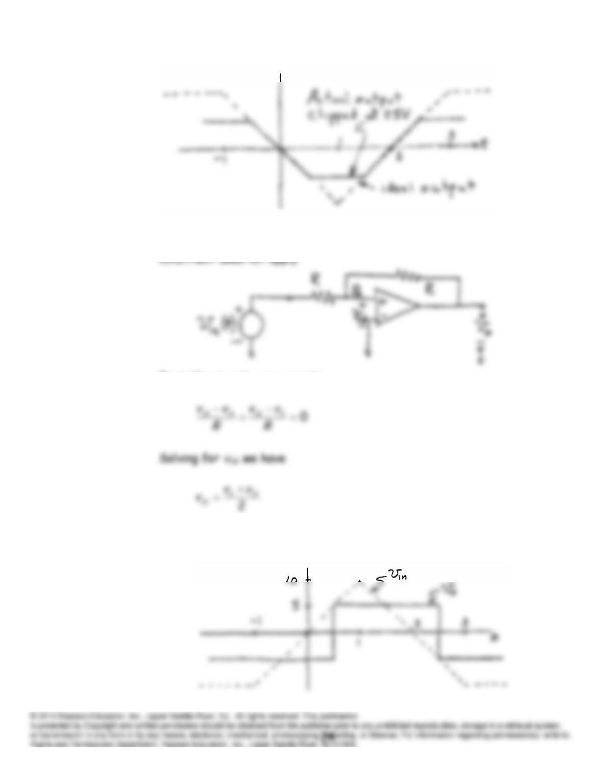
(b) This circuit has positive feedback. Therefore, the summing-point
From the circuit, we can write
If
vid
> 0, then
vo
= +5. On the other hand, if
vid
< 0, then
vo
= -5.
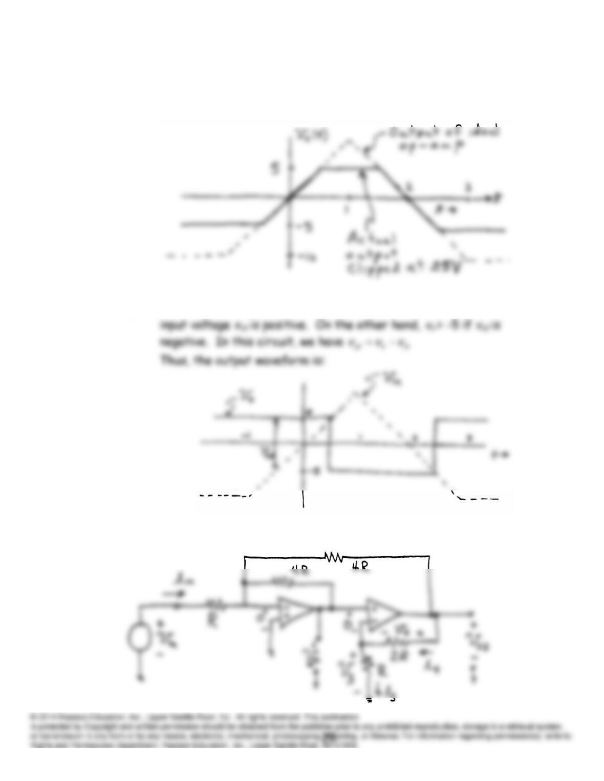
The output waveform is
P14.31 (a) This circuit has negative feedback. It is the voltage follower and
has unity gain except that the output voltage cannot exceed 5 V.
The output waveform is:
(b) This circuit has positive feedback, and
vo
= +5 if the differential
P14.32
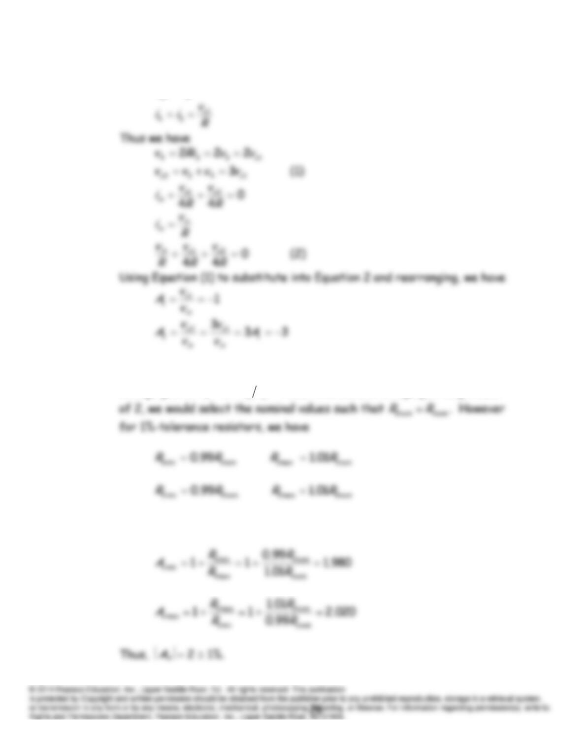
From the circuit we can write:
31
vvo
P14.33 The noninverting amplifier is shown in Figure 14.11 in the text, and the
voltage gain is
12
1
RRAv
. Thus, to achieve a voltage gain magnitude
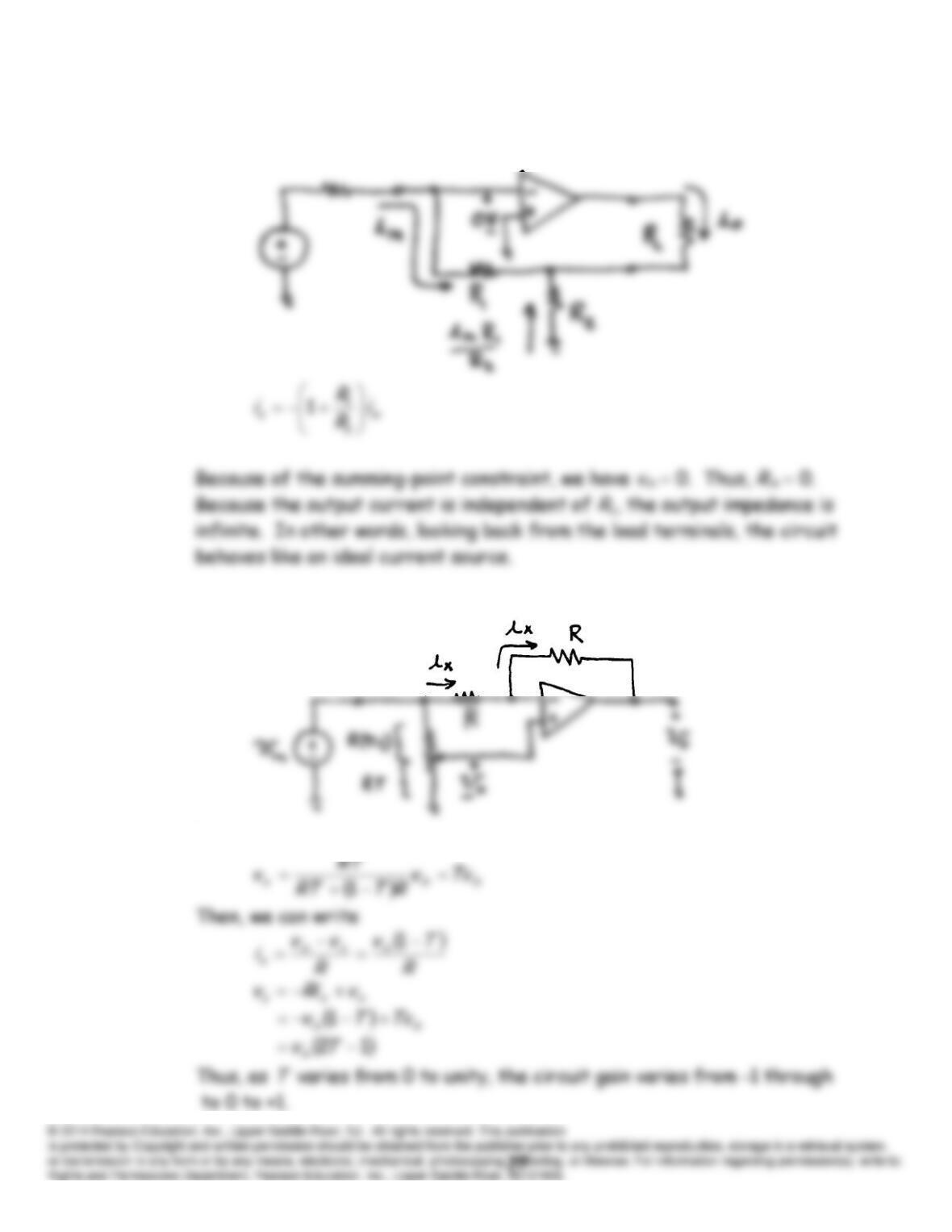
Thus we have
P14.34* The circuit diagram is:
P14.35
By the voltage-division principle, we have
P14.36 Very small resistances lead to excessively large currents, possibly
P14.37* To achieve high input impedance and an inverting amplifier, we cascade a
noninverting stage with an inverting stage:
The overall gain is:
Many combinations of resistance values will achieve the given
specifications. For example:
P14.38* A solution is:
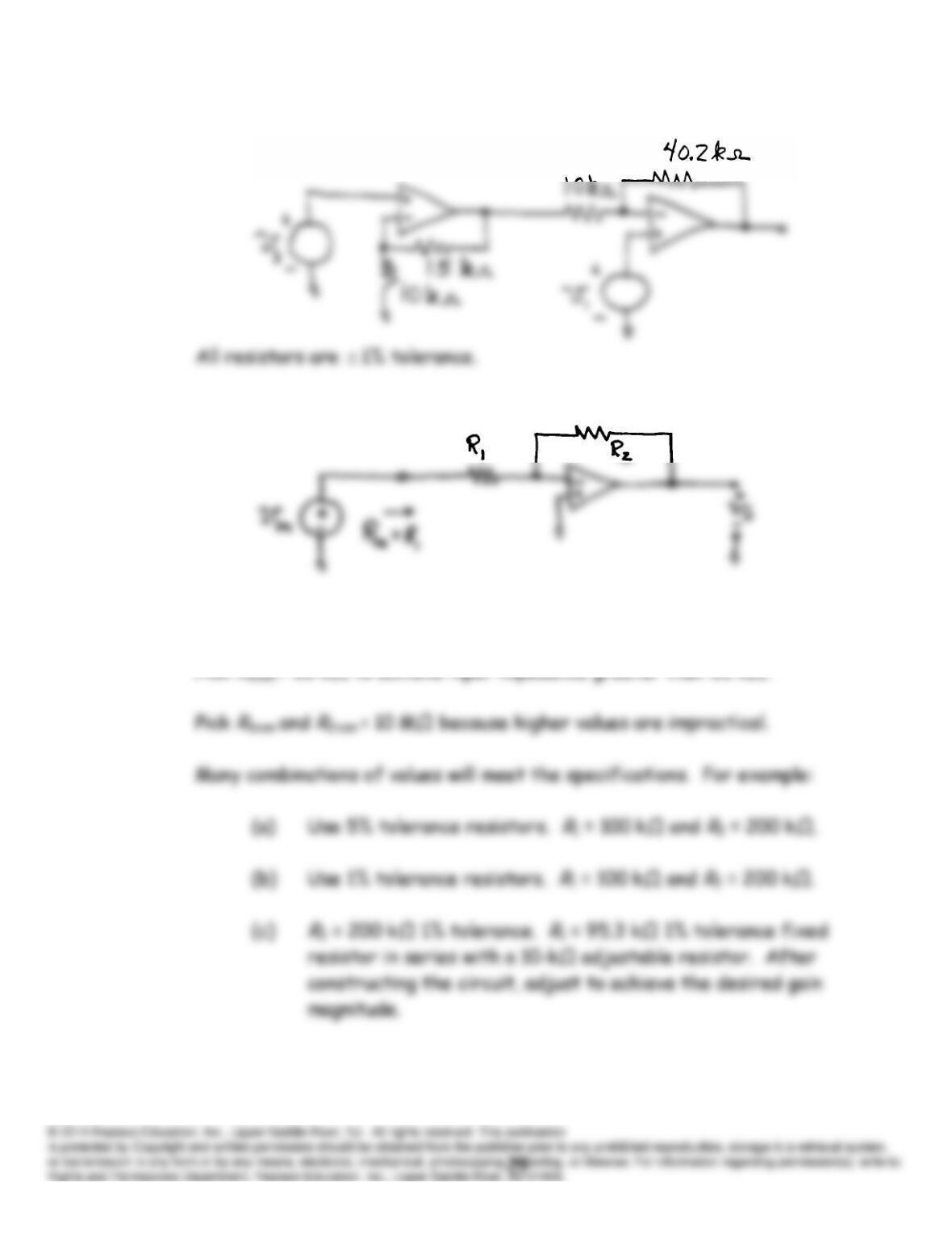
P14.39* One possibility is:
P14.40 Use the inverting amplifier configuration:
Pick
R
2nom
= 2
R
1nom to achieve the desired gain magnitude.
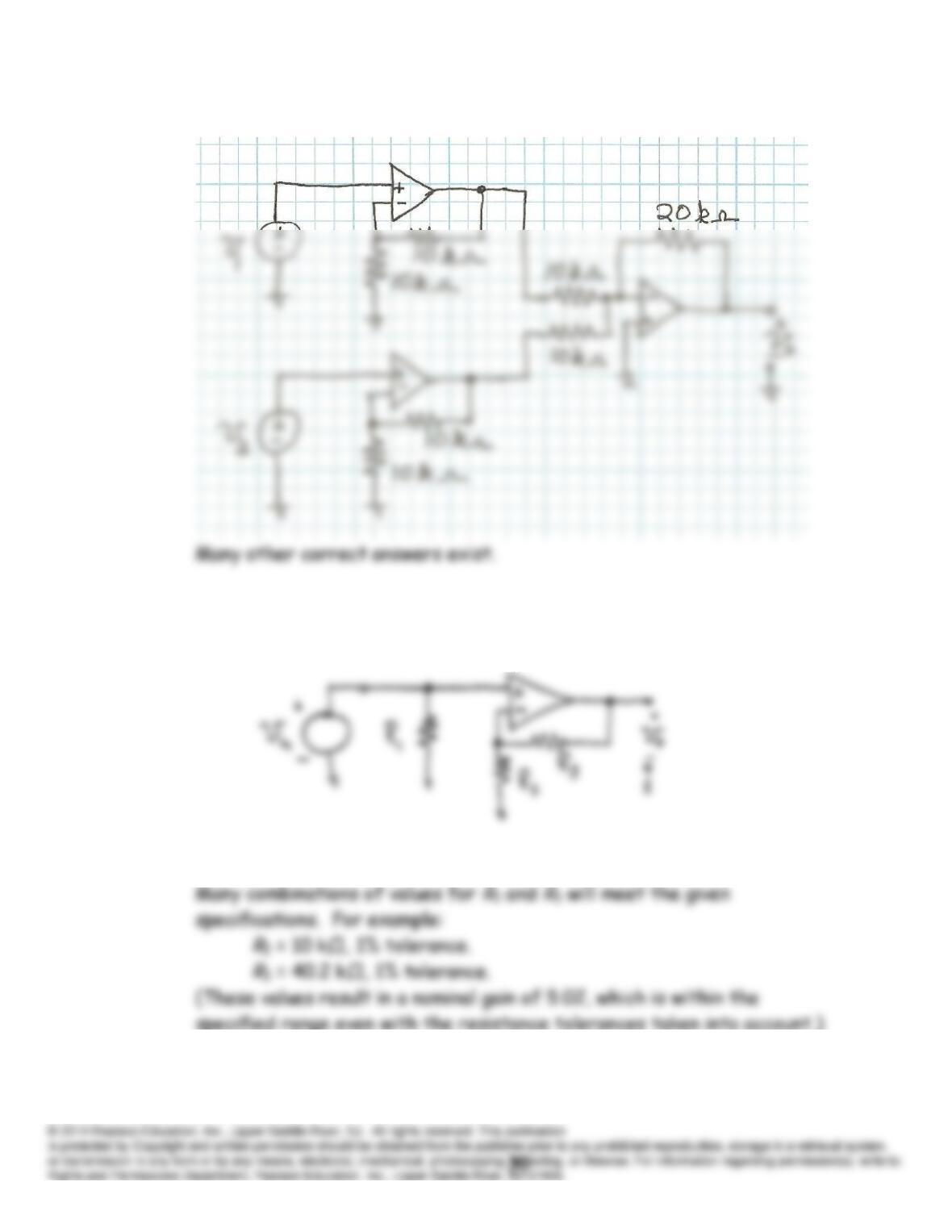
P14.41 Here is one answer in which all of the resistors have 1% tolerance:
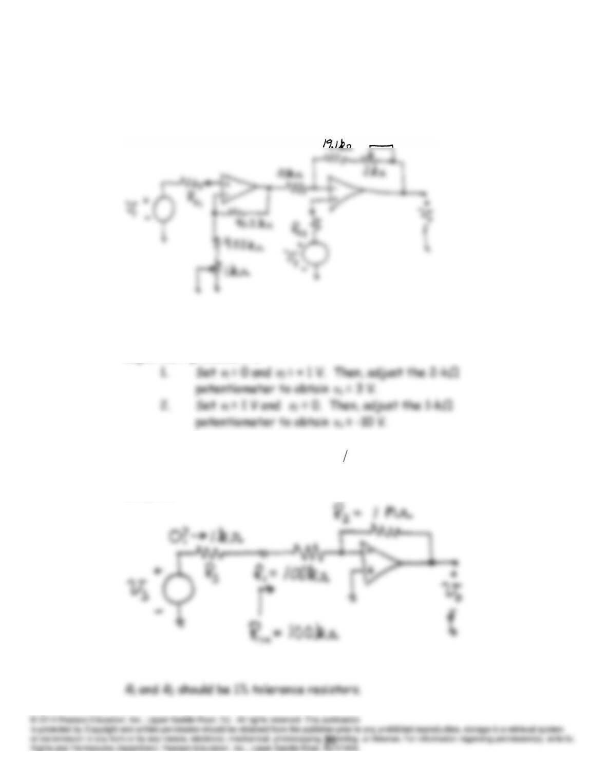
P14.42 We use a noninverting amplifier and place a resistor in parallel with the
input terminals to achieve the desired input impedance.
R
1 = 2 kΩ, 1% tolerance.
P14.43 To avoid excessive gain variations because of changes in the source
resistances, we need to have input resistances that are much greater
than the source resistances. Many correct answers exist. Here is one
possibility:
The fixed resistors should be specified to have a tolerance of
1%
because they are more stable in value than 5% tolerance resistors. The
adjustment procedure is:
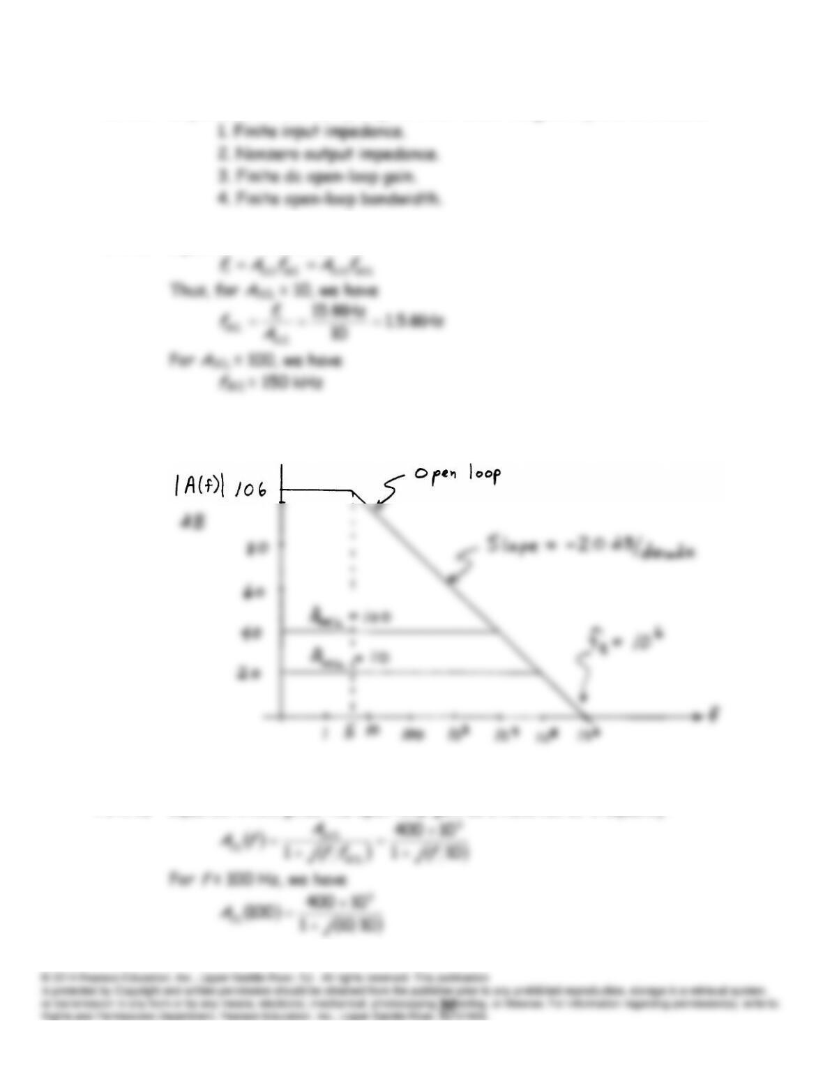
P14.44 To avoid excessive variations in
sovs vvA
because of changes in
Rs
, we
need to have
s
in RR
.
Rin
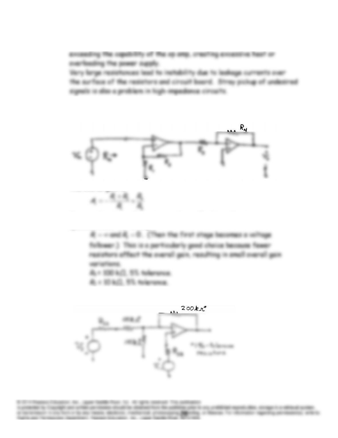
=100 kΩ is sufficiently large. Thus, a suitable
circuit is
P14.45 Imperfections of real op amps in their linear range of operation include:
P14.46* Equation 14.34 states:
P14.47*
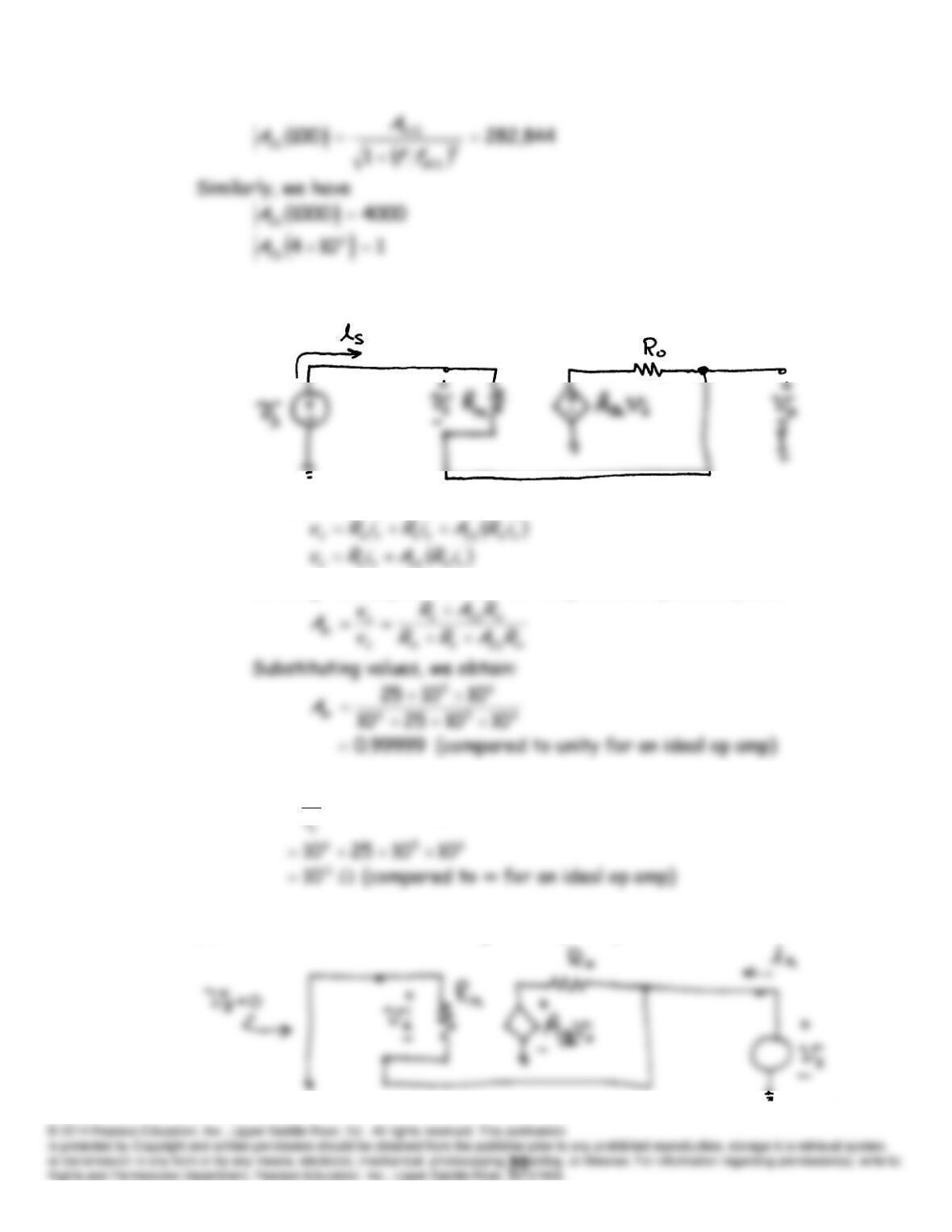
P14.48 Equation 14.23 gives the open-loop gain as a function of frequency:
P14.49 (a)
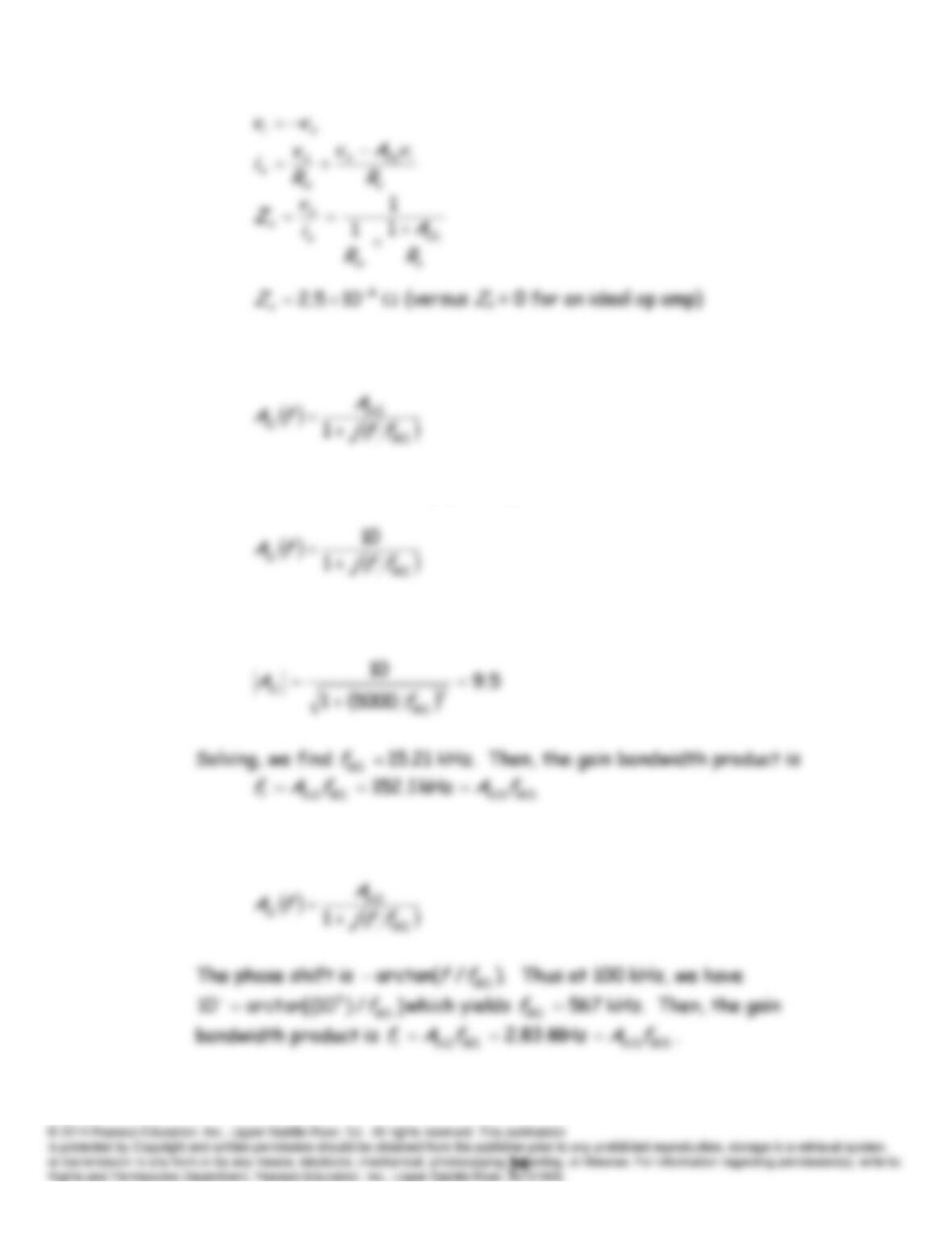
From the circuit, we can write:
Dividing the respective sides of the previous equations yields:
(b)
in
OL
o
in
s
in RARR
v
Z
(c) The circuit for determining the output impedance is:
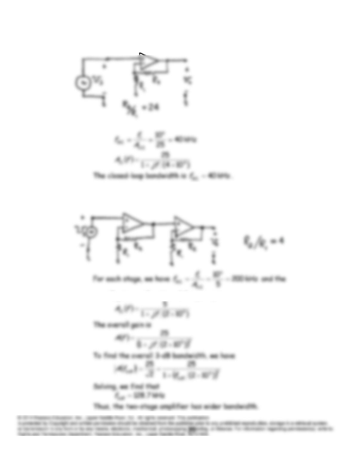
P14.50 Equation 14.32 gives the closed-loop gain as a function of frequency:
However, the dc closed-loop gain is given as 10 so we have
For
f
= 5 kHz, we have
P14.51 Equation 14.32 gives the closed-loop gain as a function of frequency:
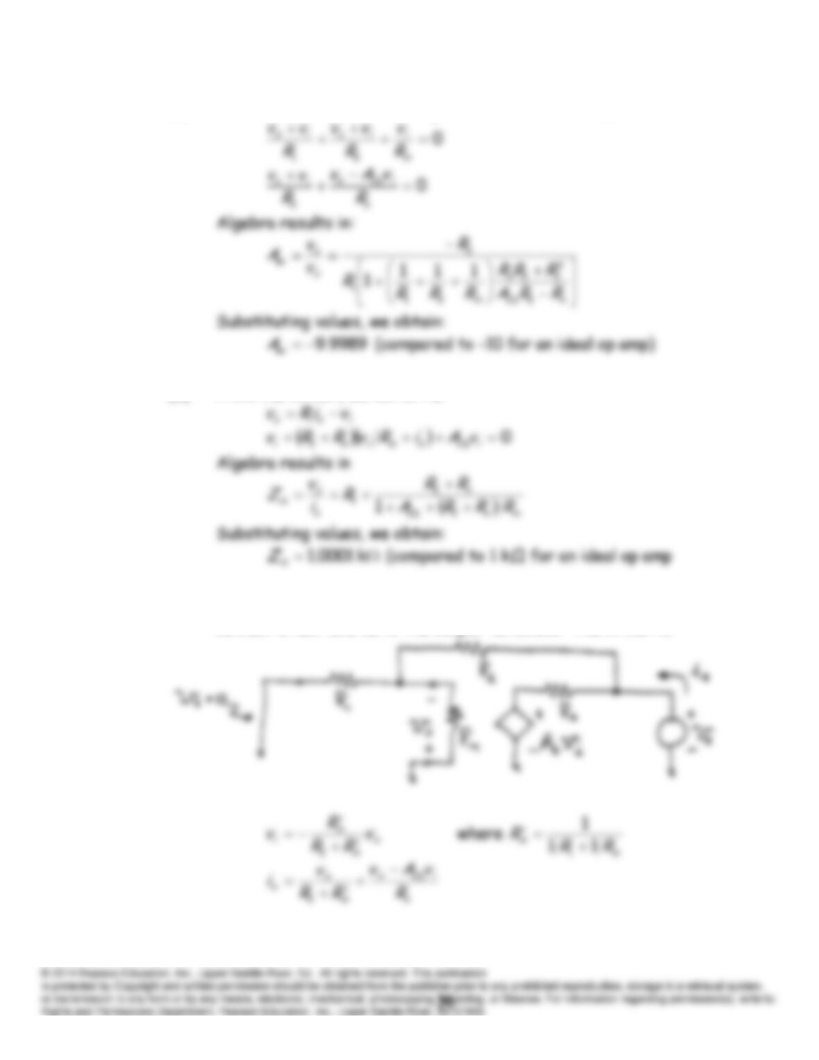
P14.52 Alternative 1:
Alternative 2:
overall gain as a function of frequency is:
P14.53 (a) From the circuit (shown in Figure P14.53 in the text), we can write:
(b) From the circuit, we can write:
(c) To find the output impedance, we zero the input source and
connect a test source to the output terminals. The circuit is:
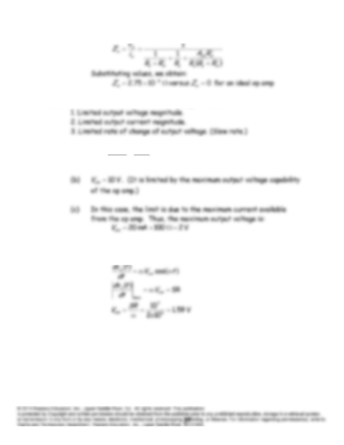
P14.54 The nonlinear limitations of real op amps include:
P14.55* (a)
kHz 159
102
10
2
7 ππ
om
FP V
SR
f
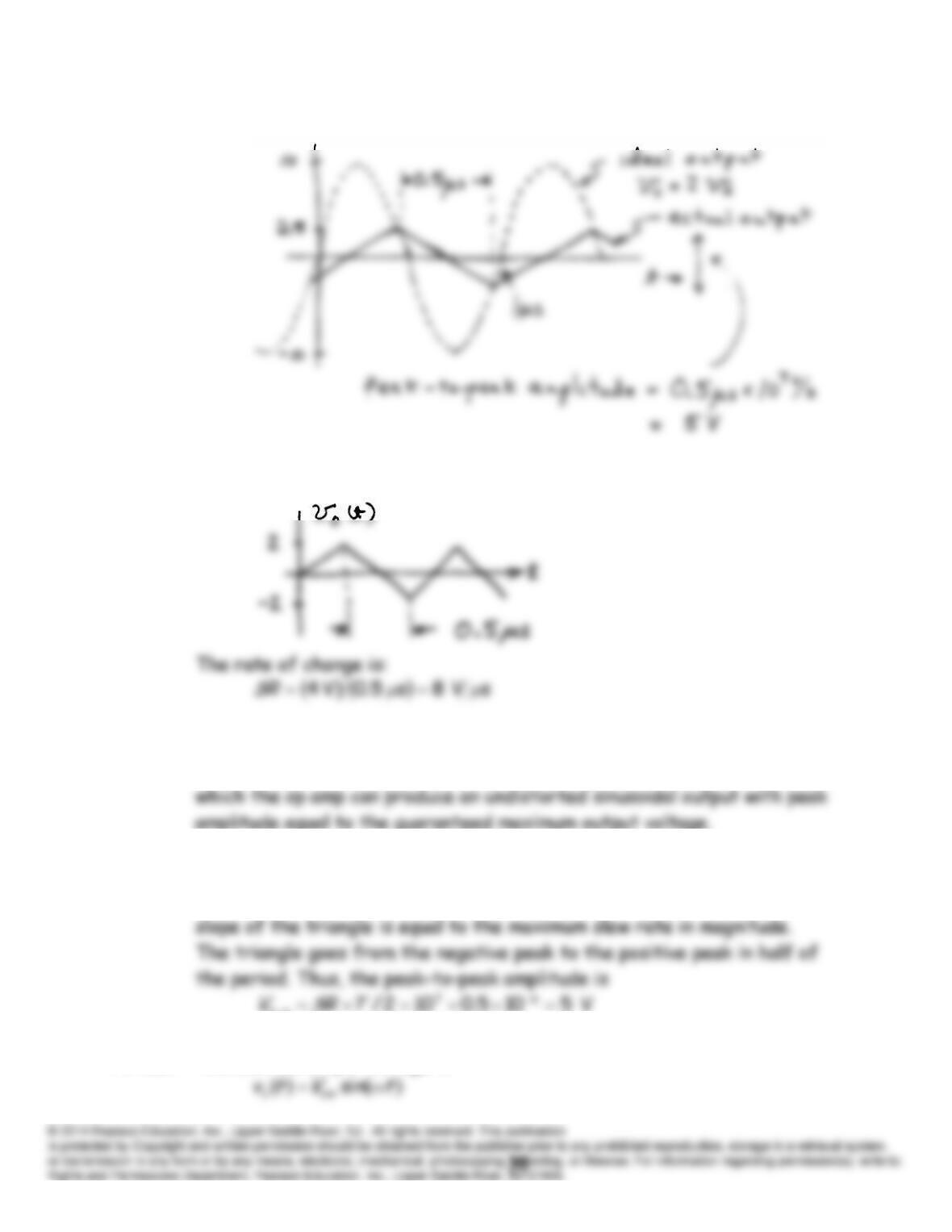
(d) In this case, the slew-rate is the limitation.
tVtv omo
ωsin
(e)
P14.56* The output waveform is
P14.57 The full-power bandwidth of an op amp is the range of frequencies for
P14.58 If the ideal output, with a sinusoidal input signal, greatly exceeds the
full-power bandwidth, the output becomes a triangular waveform. The
P14.59 The desired output voltage is