CHAPTER 14
Exercises
E14.1
(a)
A
A
AR
v
i
B
B
BR
v
i
B
B
A
A
B
A
FR
v
R
v
iii
E14.2 (a)
1
(b)
E14.3
E14.4 (a)
in
in
(b)
(Note: We assume that
.
321
RRR
)
in
E14.5
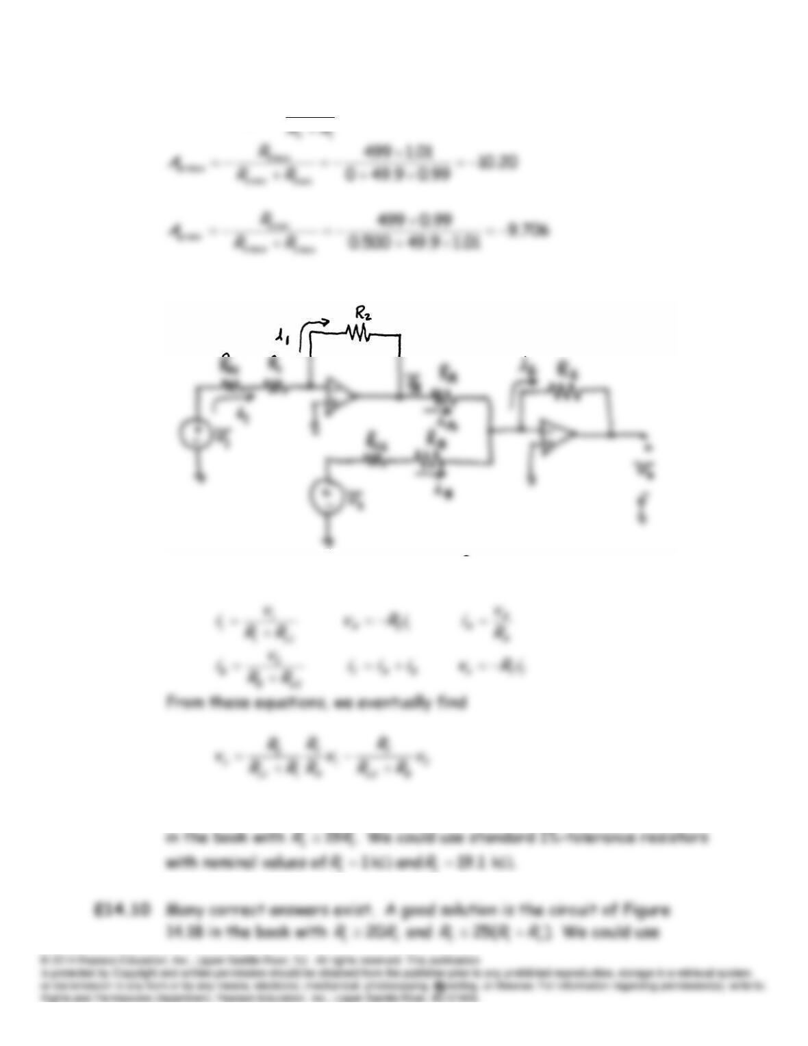
E14.6 (a)
Using the above equations we eventually find that
E14.7 We have
2
R
A
vs
from which we conclude that
E14.8
Applying basic circuit principles, we obtain:
E14.9 Many correct answers exist. A good solution is the circuit of Figure 14.11
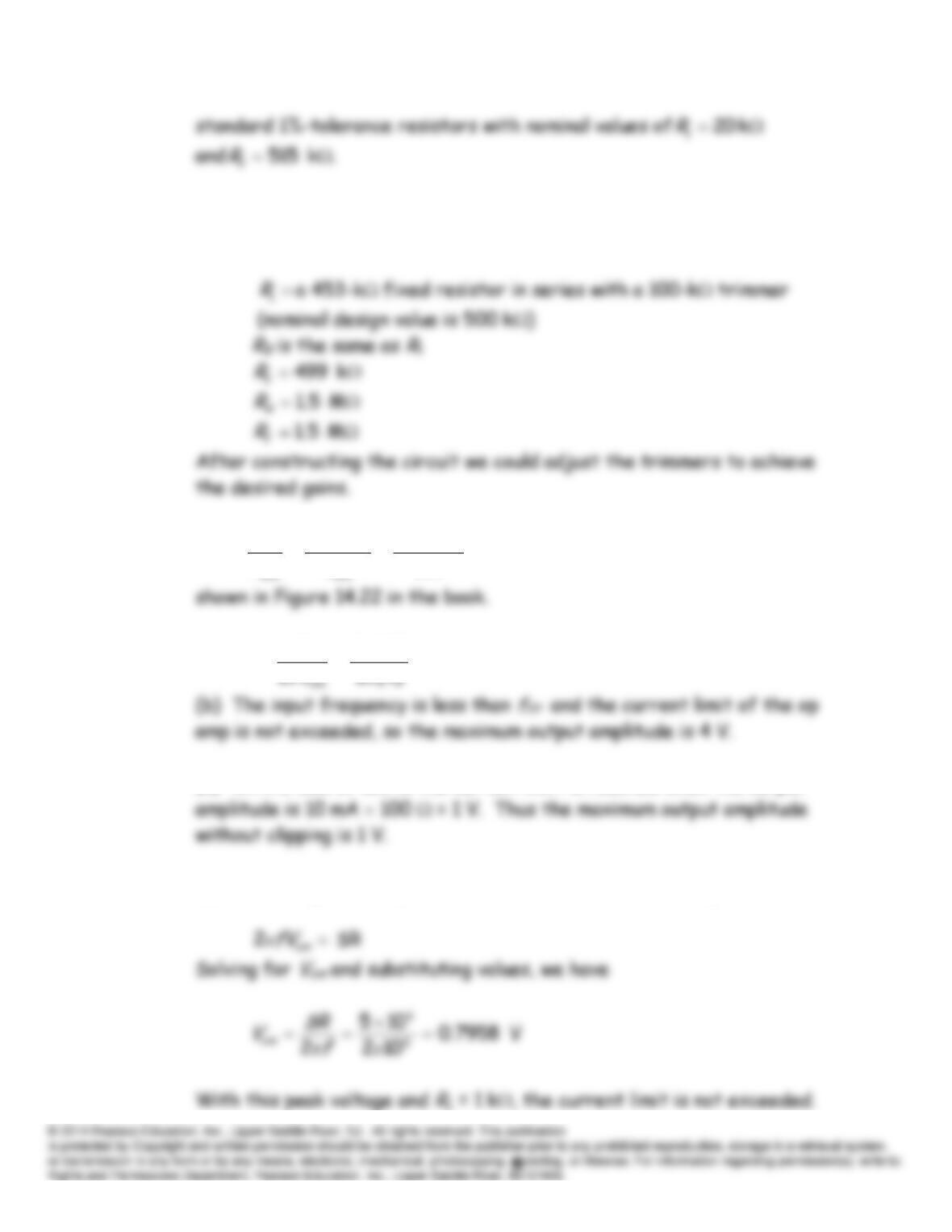
E14.11 Many correct selections of component values can be found that meet the
desired specifications. One possibility is the circuit of Figure 14.19 with:
E14.12
kHz 40
100
40105
0
0
0
CL
BOLOL
CL
t
BCL A
fA
A
f
f
The corresponding Bode plot is
E14.13 (a)
kHz 9.198
105
SR 6
ππ
FP V
f
(c) With a load of 100 the current limit is reached when the output
(d) In deriving the full-power bandwidth we obtained the equation:
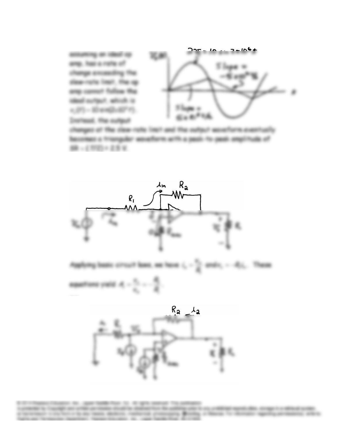
(e) Because the output,
E14.14 (a)
(b)
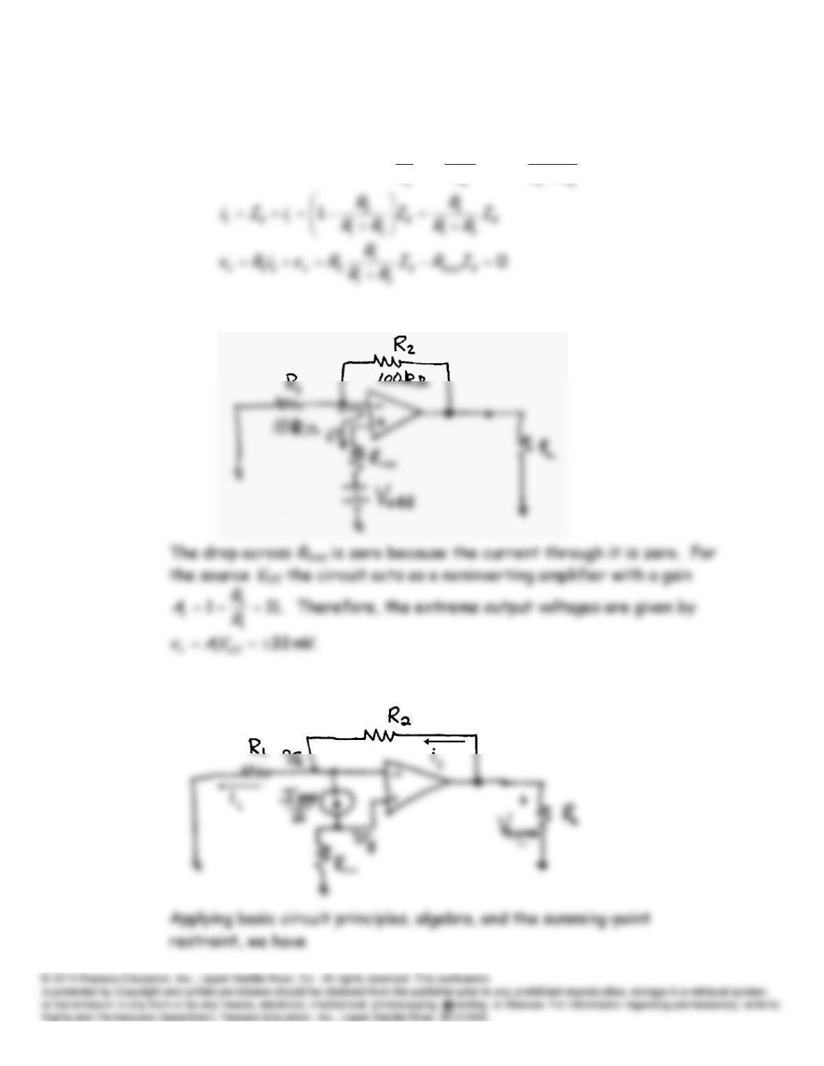
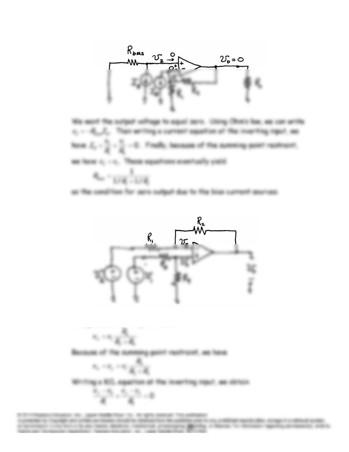
Applying basic circuit principles, algebra, and the summing-point
restraint, we have
B
bias
yx IRvv
BB
bias
xI
RR
R
I
R
R
R
v
i
2
1
(c)
(d)
off
I
off
2
off
I
R
I
R
v
x
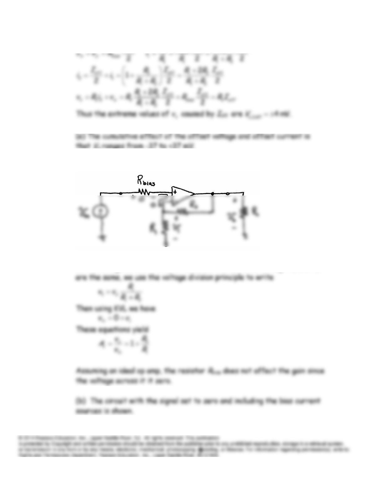
E14.15 (a)
Because of the summing-point constraint, no current flows through
R
bias
so the voltage across it is zero. Because the currents through
R
1 and
R
2
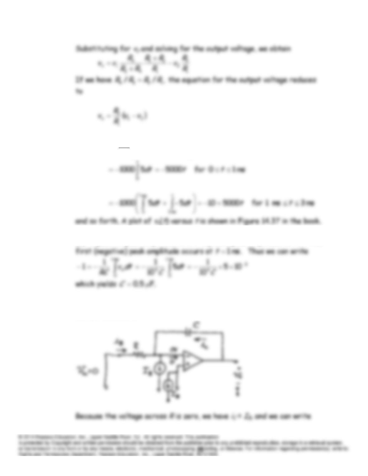
E14.16
Because no current flows into the op-amp input terminals, we can use the
voltage division principle to write
E14.17 (a)
tt
odttvdttv
RC
tv
0
in
0
in )(1000)(
1
)(
(b) A peak-to-peak amplitude of 2 V implies a peak amplitude of 1 V. The
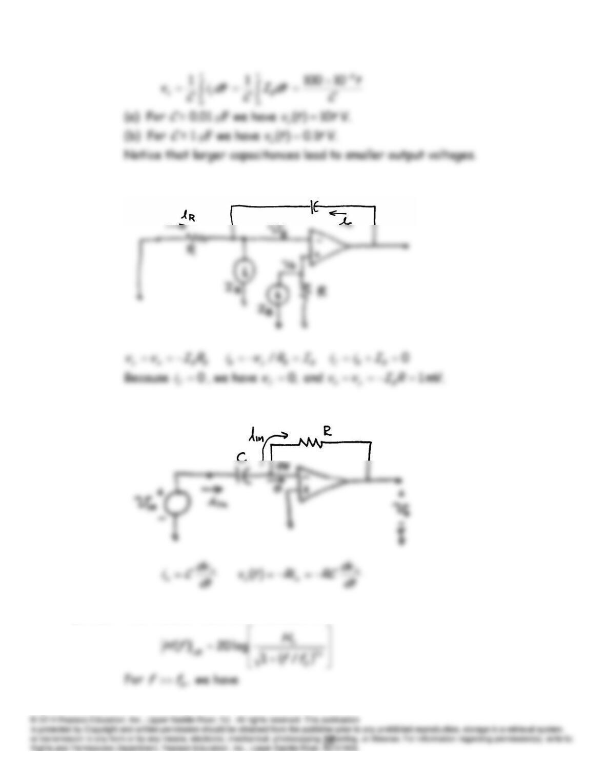
E14.18 The circuit with the input source set to zero and including the bias
current sources is:
E14.19
E14.20
E14.21 The transfer function in decibels is
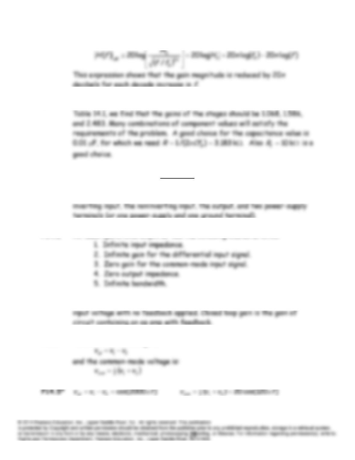
E14.22 Three stages each like that of Figure 14.40 must be cascaded. From
Problems
P14.1 The most probable functions of the five op amp terminals are the
P14.2 An ideal operational amplifier has the following characteristics:
P14.3 The open-loop gain is the voltage gain of the op amp for the differential
P14.4 The differential voltage is:
P14.6* The steps in analysis of an amplifier containing an ideal op amp are:
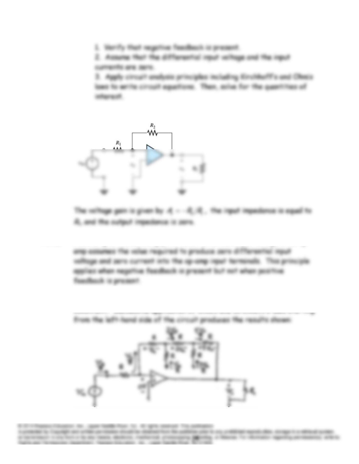
P14.7 The inverting amplifier configuration is shown in Figure 14.4 in the text.
P14.8 According to the summing-point constraint, the output voltage of an op
P14.9* The circuit has negative feedback so we can employ the summing-point
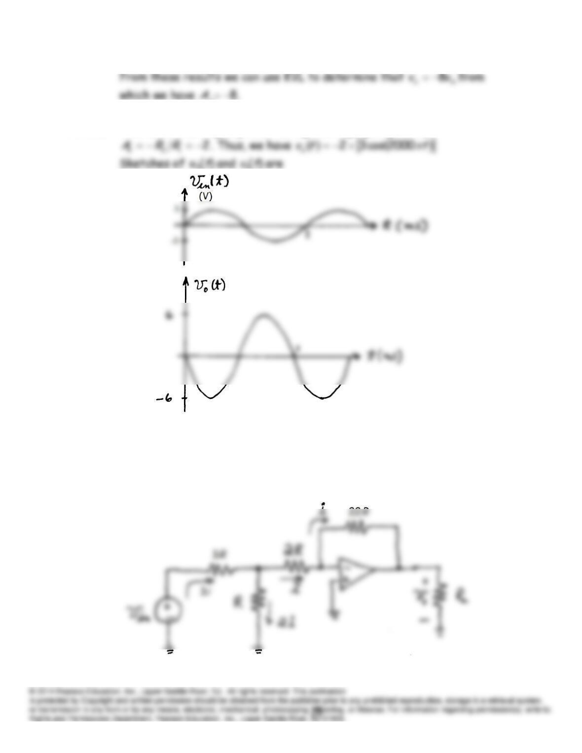
v
P14.10 This is an inverting amplifier having a voltage gain given by
in(
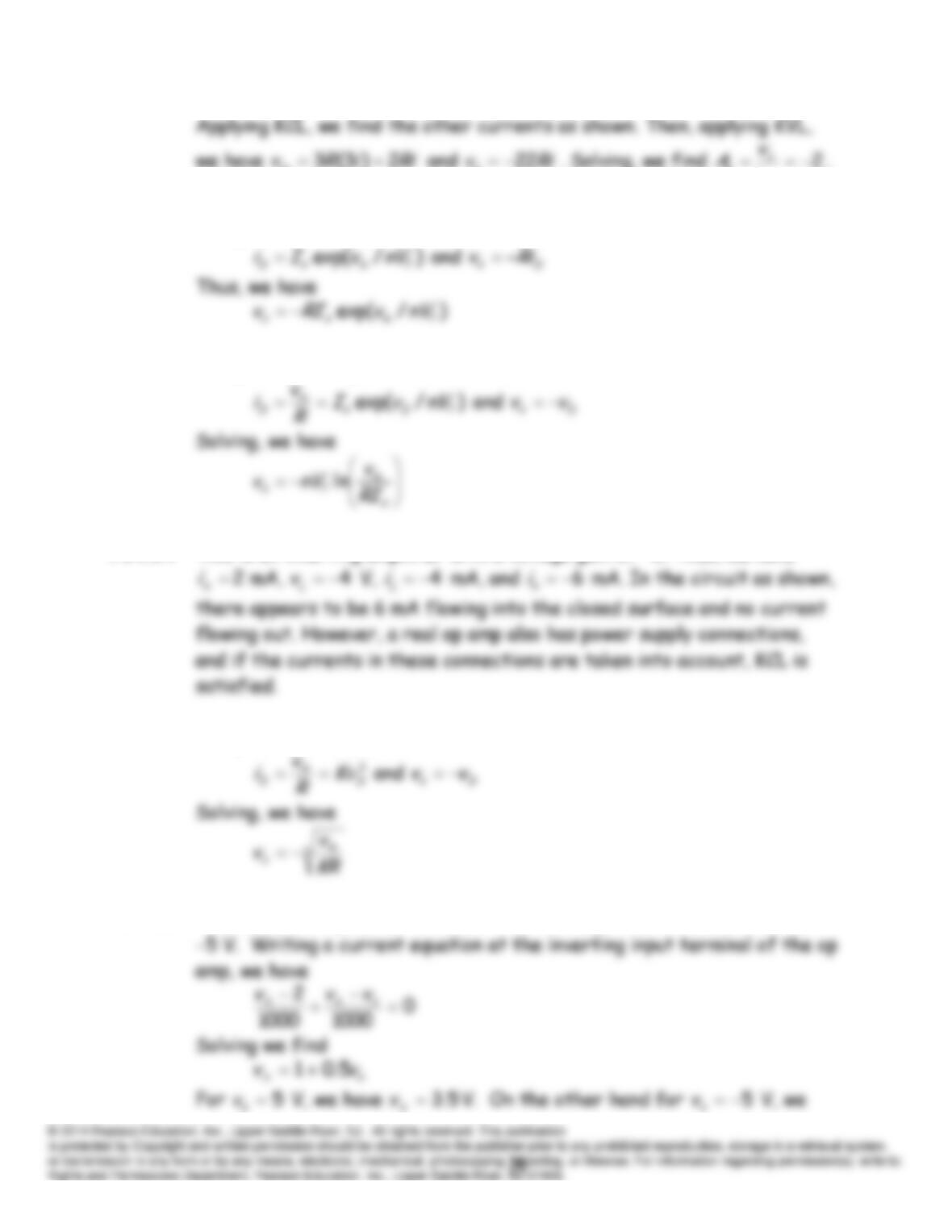
P14.11 Because of the summing-point constraint, the voltages across the
resistors of values
R
and 2
R
are equal. Thus, the current in the resistor
of value
R
is twice that of the current in the 2
R
resistor as indicated:
in
vv
P14.12 Using the summing-point constraint, we have
P14.13 Using the summing-point constraint, we have
P14.14 This is an inverting amplifier with a voltage gain of 2. Thus, we have
P14.15 Using the summing-point constraint, we have
P14.16 This circuit has positive feedback and the output can be either +5 V or
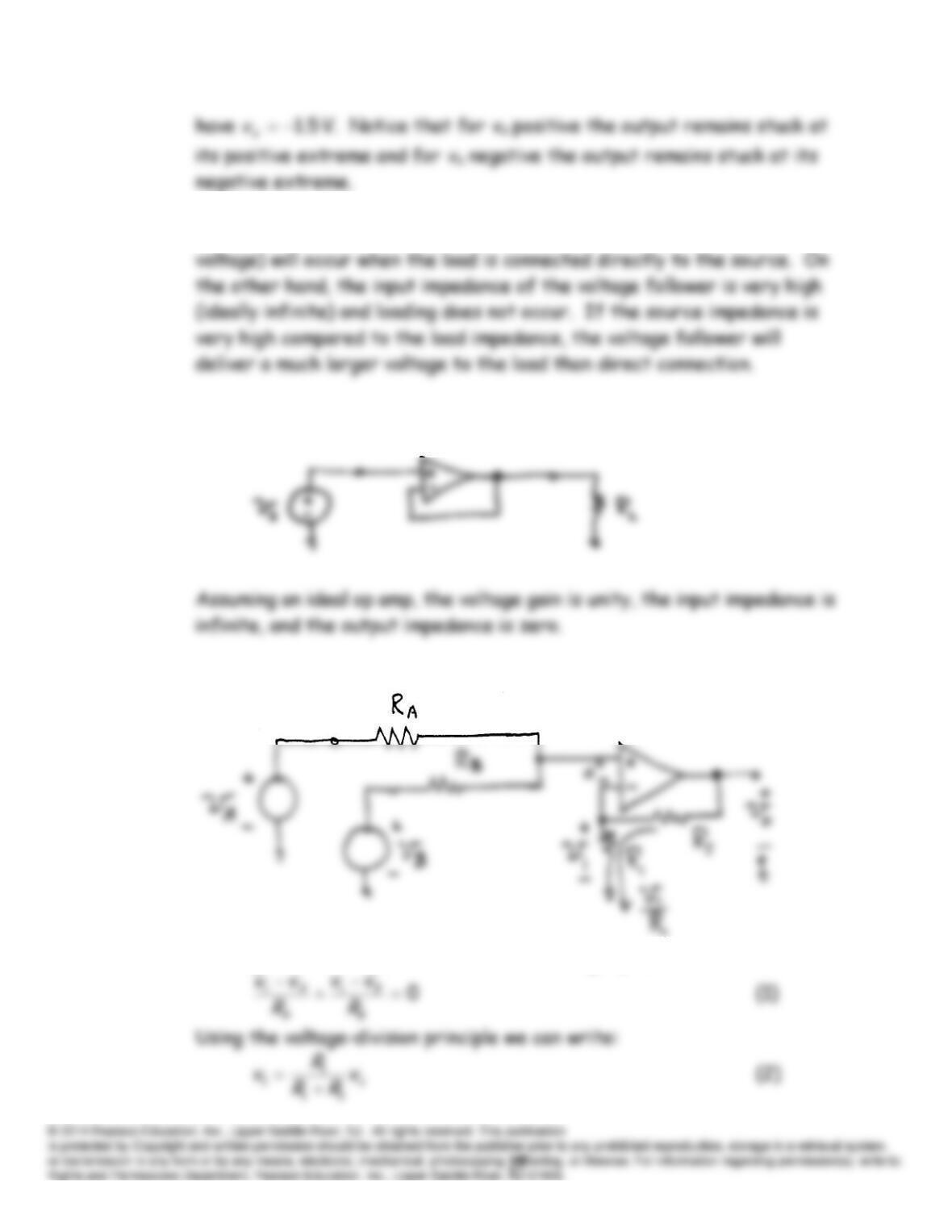
P14.17* If the source has non-zero series impedance, loading (reduction in
P14.18* The circuit diagram of the voltage follower is:
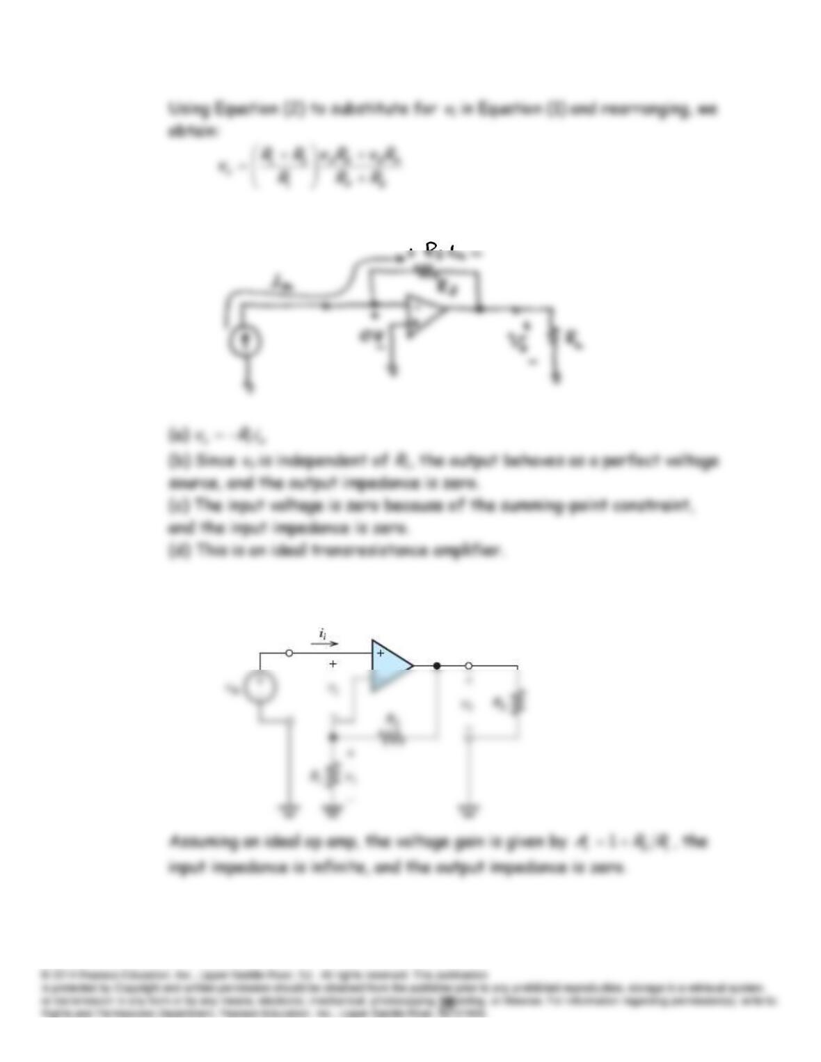
P14.19* The circuit diagram is:
Writing a current equation at the noninverting input, we have
P14.20*
P14.21 The noninverting amplifier configuration is shown in Figure 14.11 in the
text.
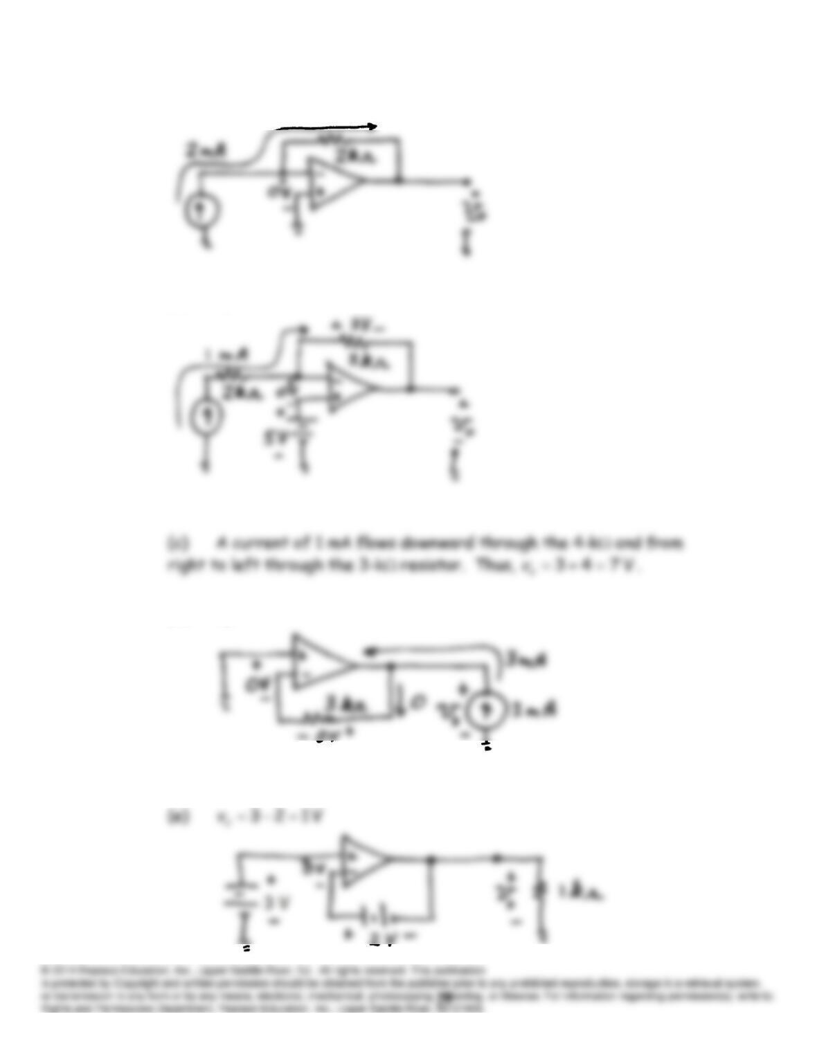
P14.22 (a)
V 4mA 2k 2
o
v
(b)
V 2503
o
v
(d)
0
o
v
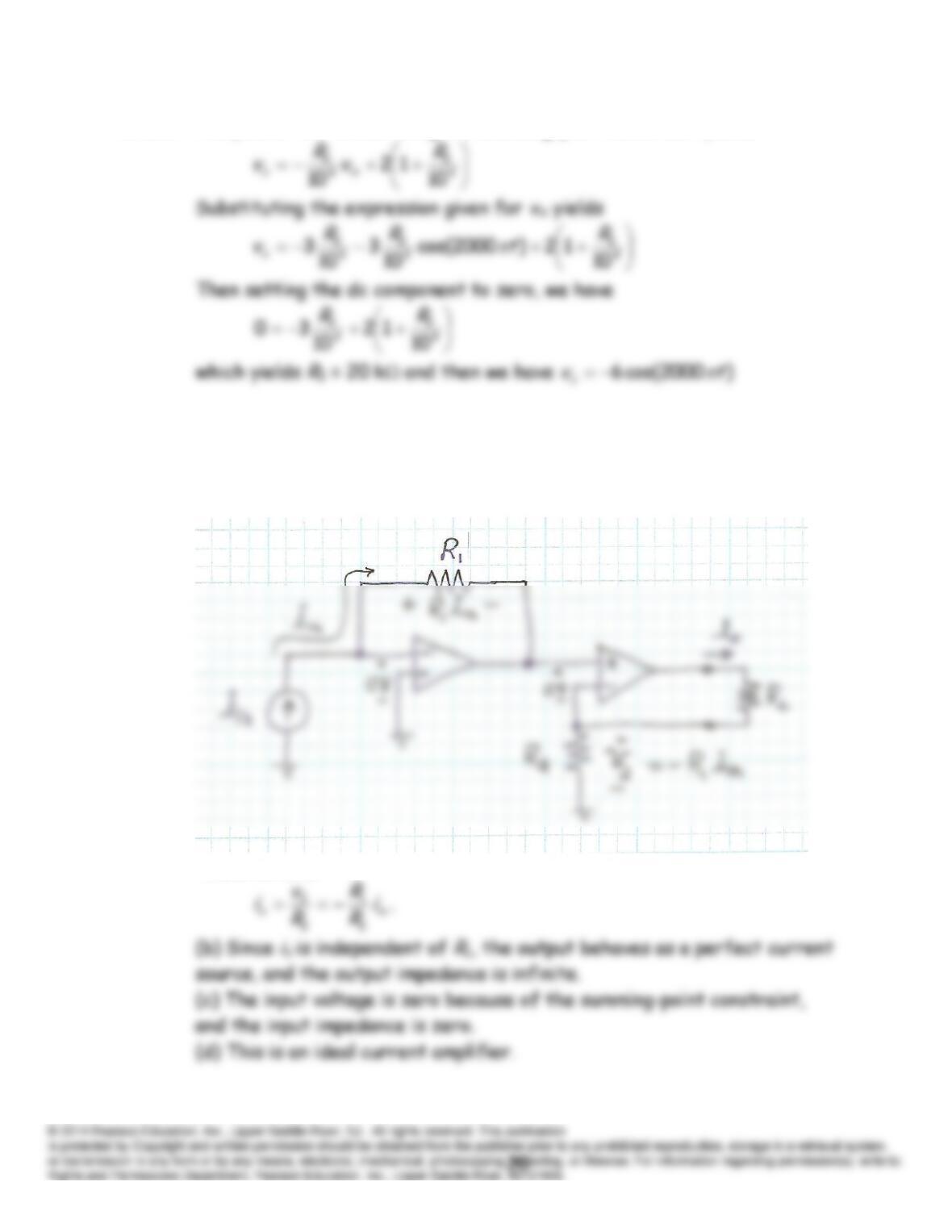
P14.23 Analysis of the circuit using the summing-point constraint yields
P14.24 (a) Working from left to right, we find the currents and voltages as
shown:
Then, we have