P13.29*
P13.30 We can write
P13.32 The magnitude of
v
is decreased by about 2 mV for each
C increase in
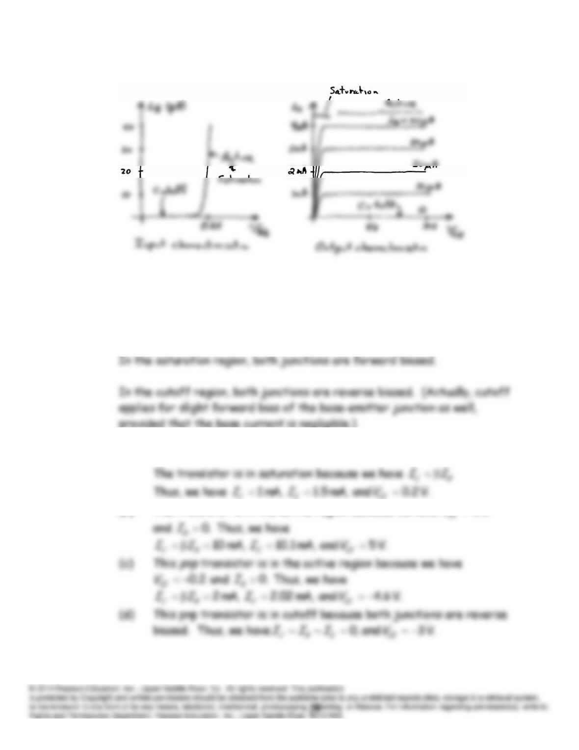
P13.33
P13.34 See Figure 13.16 in the text.
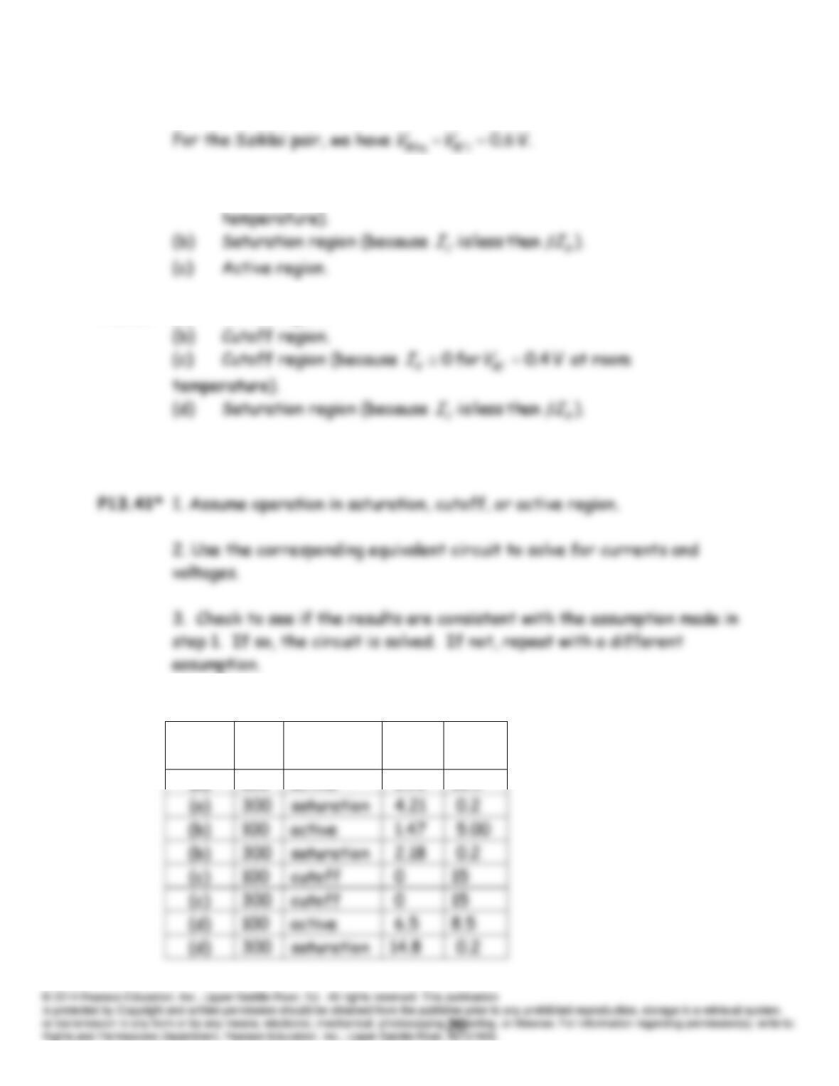
P13.35* In the active region, the base-collector junction is reverse biased and
the base-emitter junction is forward biased.
P13.36 (a)
mA 5.0
C
E
BIII
(b) The transistor is in the active region because we have
2.0
V
P13.37 For the Darlington pair, we have
V. 2.1
21eq
BEBEBE VVV
P13.38 (a) Cutoff region (because
V 3.0 for 0
BE
BVI
at room
P13.39 (a) Active region.
P13.40 See Figure 13.16 in the text.
P13.42* The results are given in the table:
Circuit
β
Region of
operation
C
I
(mA)
CE
V
(volts)
(a)
100
active
1.93
10.9
300
saturation
4.21
0.2
100
active
1.47
5.00
300
saturation
2.18
0.2
100
cutoff
0
15
300
cutoff
0
15
100
active
6.5
8.5
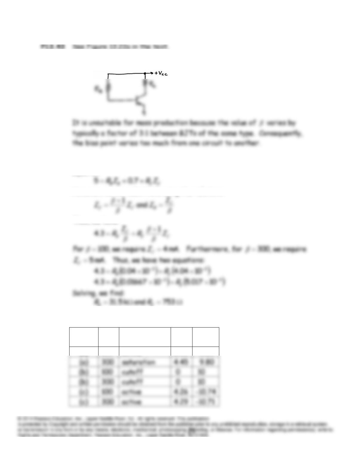
P13.44 The fixed base bias circuit is:
P13.45* The BJT operates in the active region. We can write the voltage
equation:
However, we can substitute using the relations:
Thus, we have:
E
BRR
P13.46 The results are given in the table:
Circuit
β
Region of
operation
I
(mA)
V
(volts)
(a)
100
active
2.38
5.25
100
cutoff
0
100
active
4.26
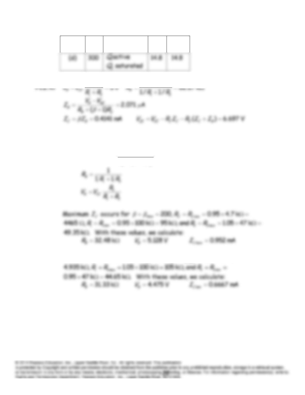
(d)
100
active
1
Q
active
2
Q
9.53
9.53
2
R
1
P13.48* From Equations 13.20 through 13.23, we have:
E
B
BE
B
B
CRR
VV
II
1
β
ββ
Minimum
C
I
occurs for
k 7.405.1 ,50 max
min
EE RR
ββ
P13.49 It turns out that for the values given the BJT operates in the saturation
region and the equivalent circuit is:
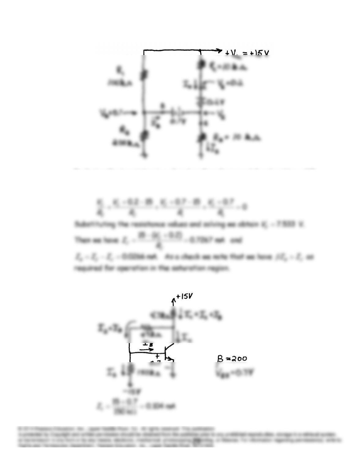
Enclosing the transistor in a closed surface (supernode) and writing a KCL
equation, we have
P13.50
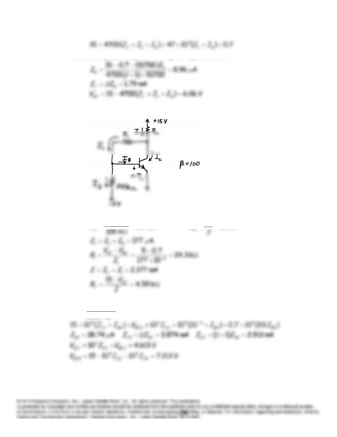
Substituting
β
and solving for
I
, we obtain:
P13.51 The circuit is:
We have:
A 157
7.015
I
A 20 μ
C
I
I
P13.52
A 10
15
6
1
1
BE
B
V
I
mA 1
1
1
B
CII
T
V
β
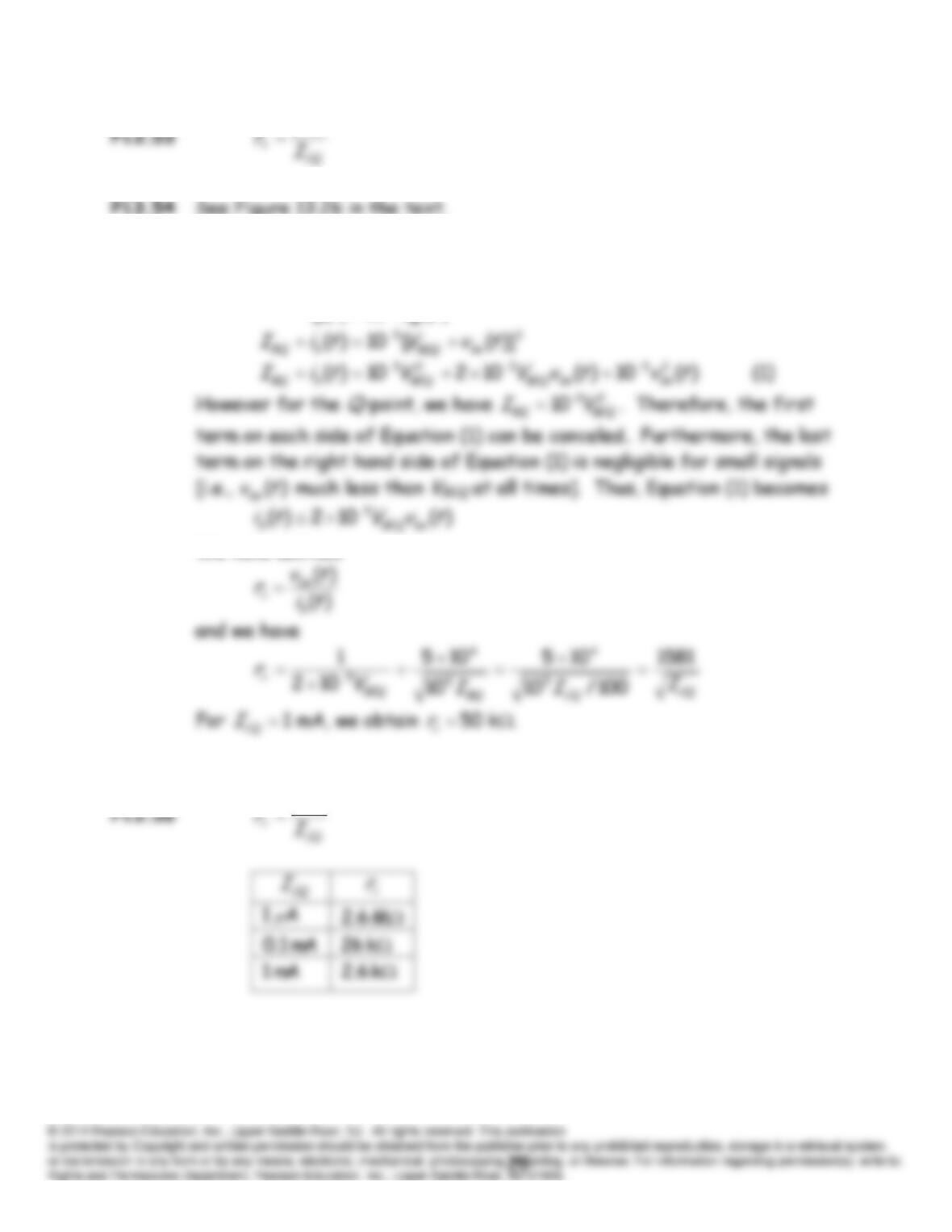
P13.55* We use the same approach as in Section 13.7. We can write
)(10)( 25
tvti BE
We have defined
T
V
β
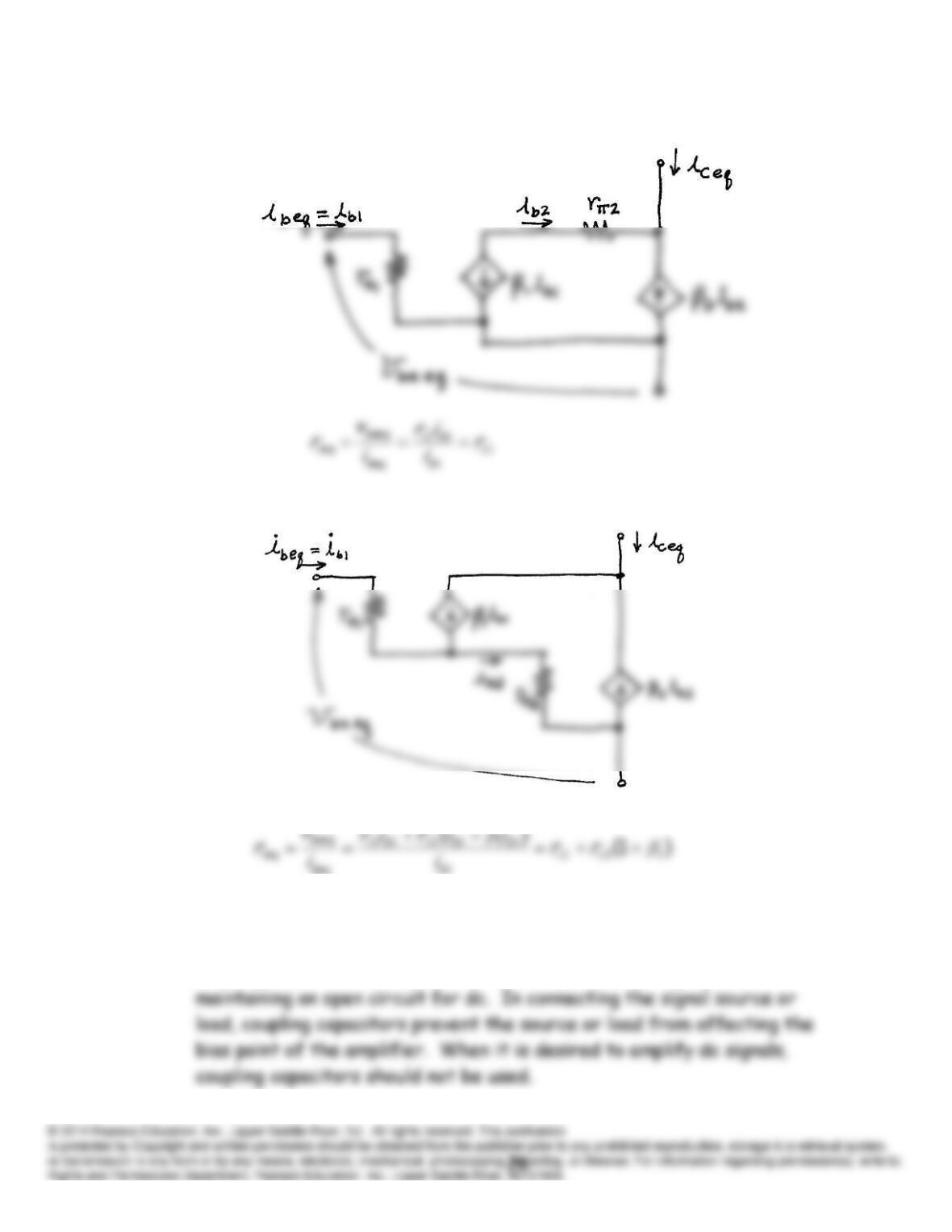
P13.57 The equivalent circuit is:
P13.58 The equivalent circuit is:
P13.59 See Figure 13.27a in the text.
P13.60 Coupling capacitors are used to provide a path for ac signals while
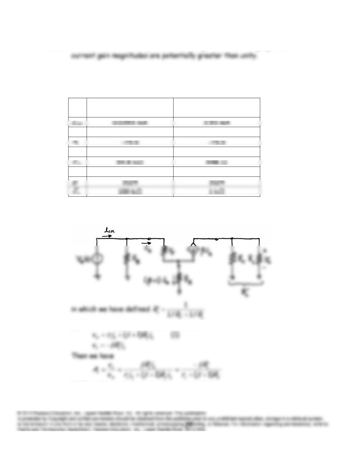
P13.61 The common-emitter amplifier is inverting. Both the voltage gain and
P13.62* The solution is similar to that of Problem P13.64. The results are:
High impedance amplifier
(Problem 13.62)
Low impedance amplifier
(Problem 13.64)
π
r
66.2 kΩ
662 Ω
v
oc
v
A
-151
-151
in
i
A
-41.4
-41.4
o
P13.63 (a) The small-signal equivalent circuit is:
(b) From the equivalent circuit we can write:
(c) From the equivalent circuit we can write:
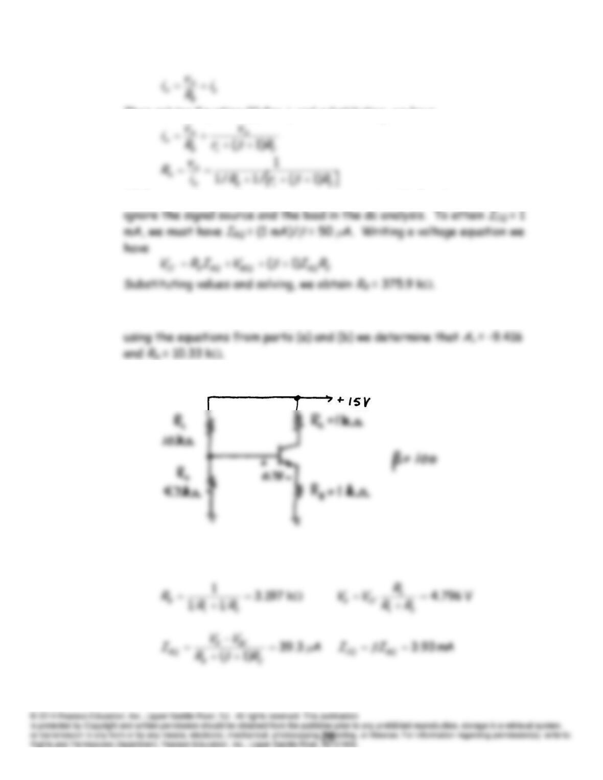
Then solving Equation (1) for
ib
and substituting, we have
(d) Because the coupling capacitors are open circuits for dc, we can
(e) First, we have
Ω 520005.0/)026.0100(/
CQ
tIVr
β
π
. Then
P13.64 The dc circuit is:
The bias point calculations are:
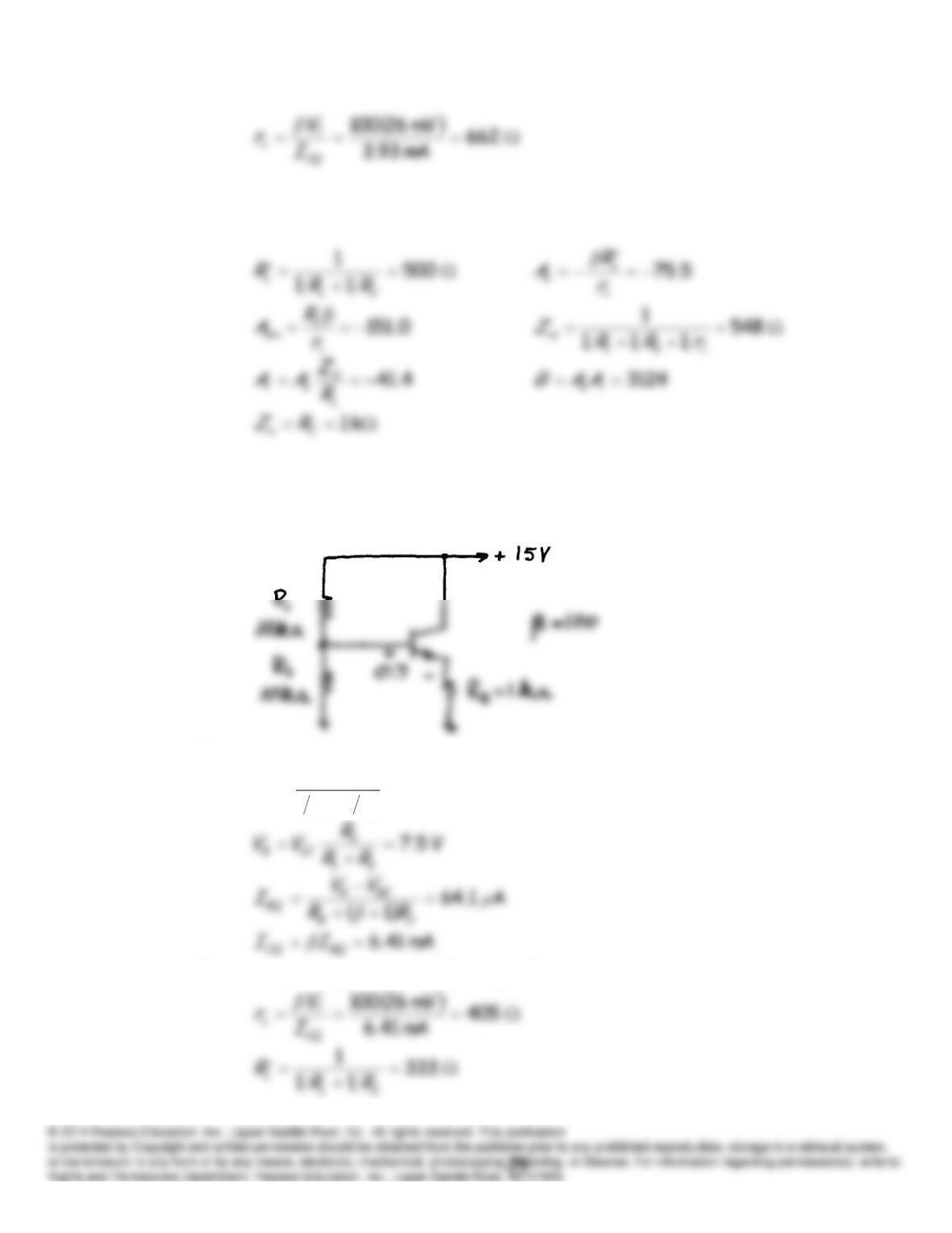
Then, we compute the amplifier performance:
P13.65 See Figure 13.30a in the text.
P13.66* The dc circuit is:
The bias point calculations are:
k 5
11
1
21
RR
RB
Now we can compute
π
r
and the ac performance.
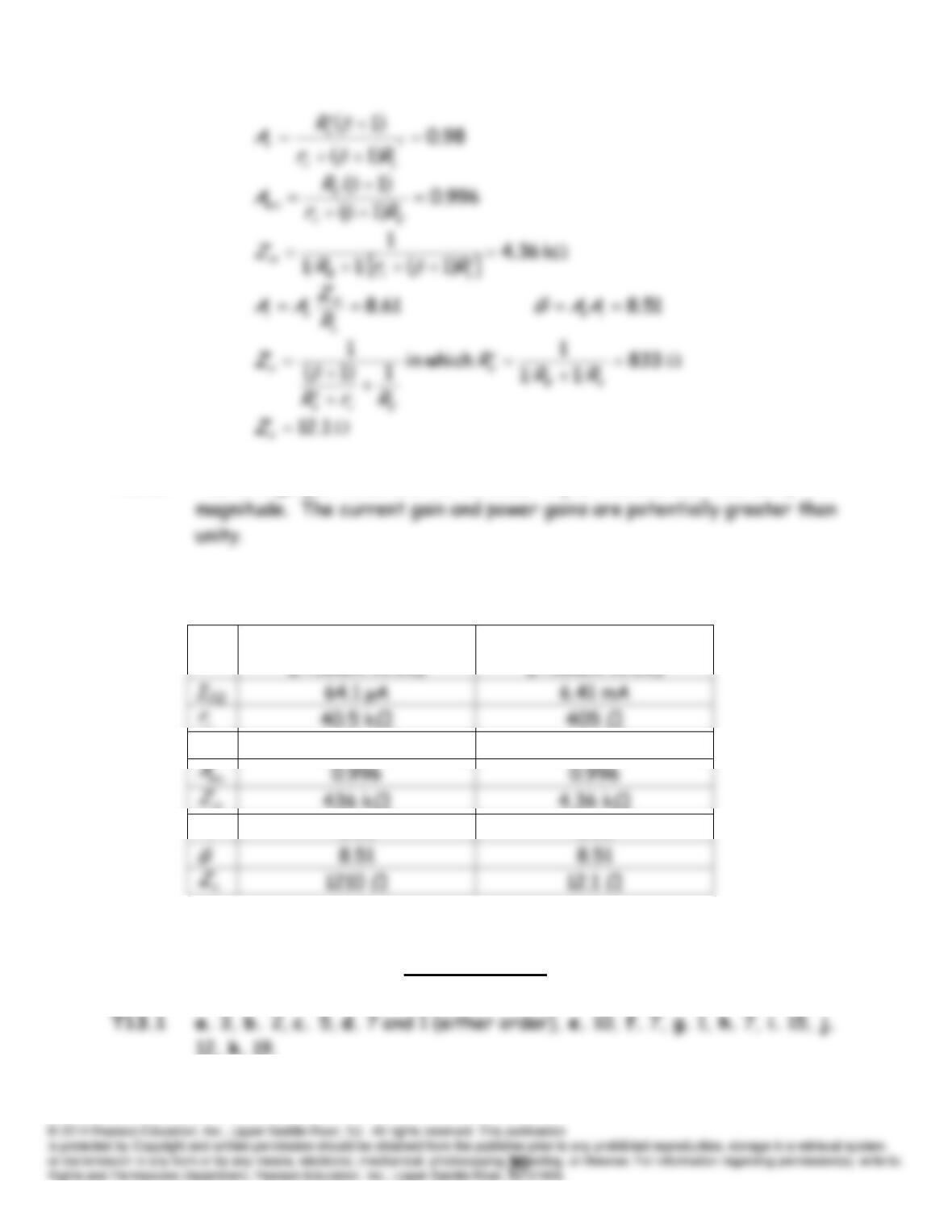
P13.67 The voltage gain of an emitter follower is positive and less than unity in
P13.68 The solution is similar to that of Problem P13.66. The results are:
High impedance amplifier
(Problem 13.68)
Low impedance amplifier
(Problem 13.66)
v
A
0.988
0.988
in
i
A
8.61
8.61
Practice Test
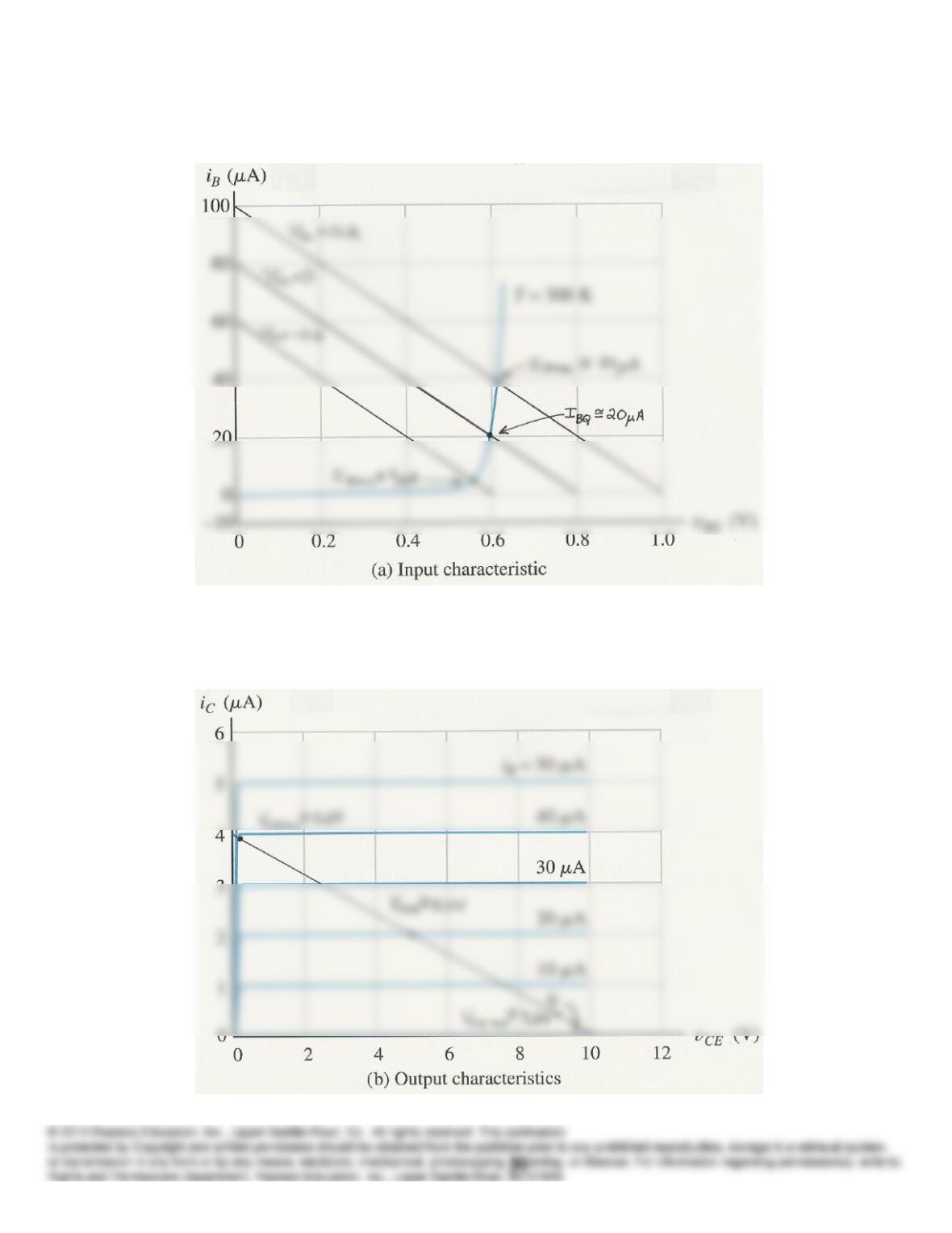
T13.2 First, we construct the load lines on the input characteristics for
v
in 0,
0.2 V, and +0.2 V:
At the intersections of the characteristic with the load lines, we find the
minimum,
Q
-point, and maximum values of the base current as shown.
Then, we construct the load line on the collector characteristics:
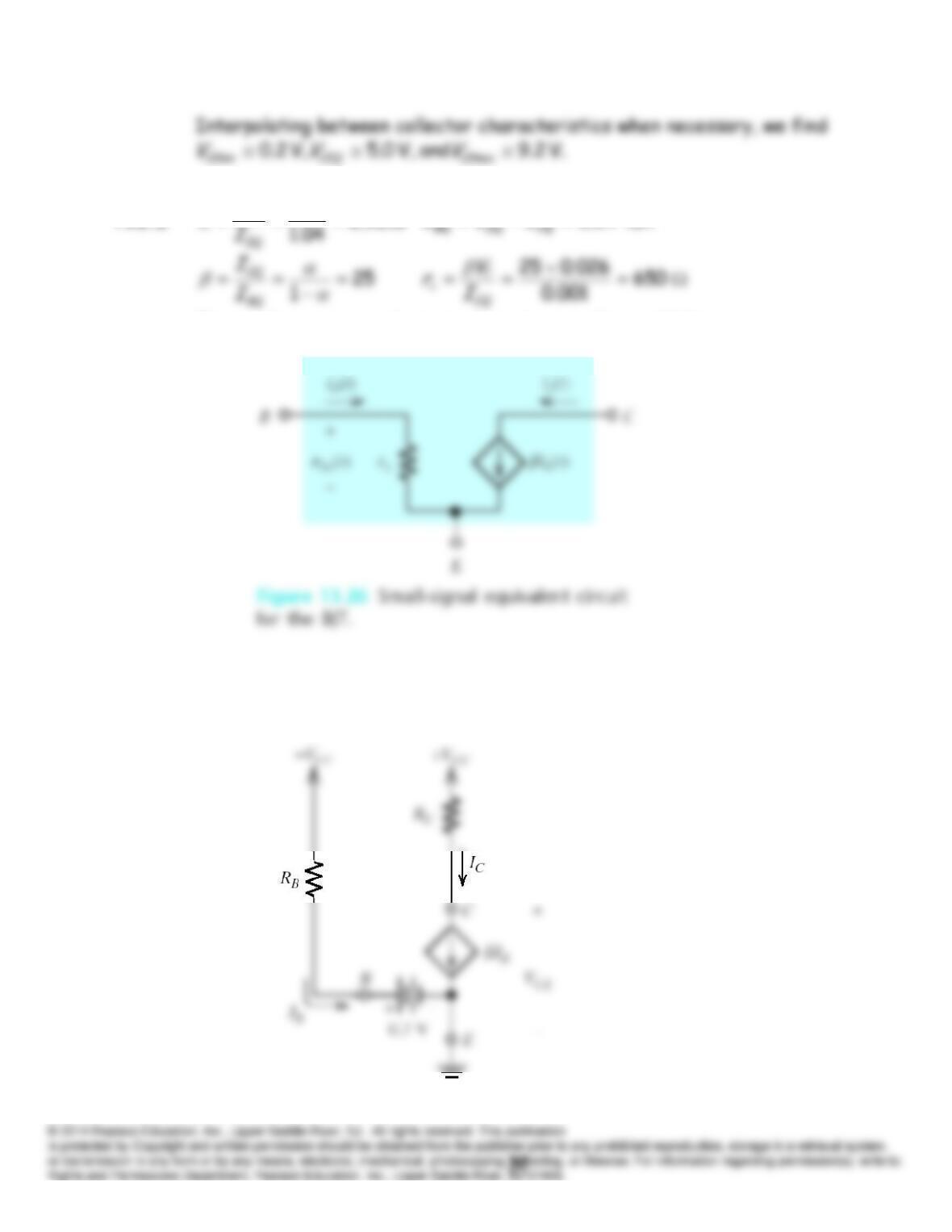
T13.3
9615.0
0.1
CQ
I
04.0
mA
The small-signal equivalent circuit is shown in Figure 13.26.
T13.4 (a) It turns out that, in this case (
),50
the BJT operates in the active
region. The equivalent circuit is:
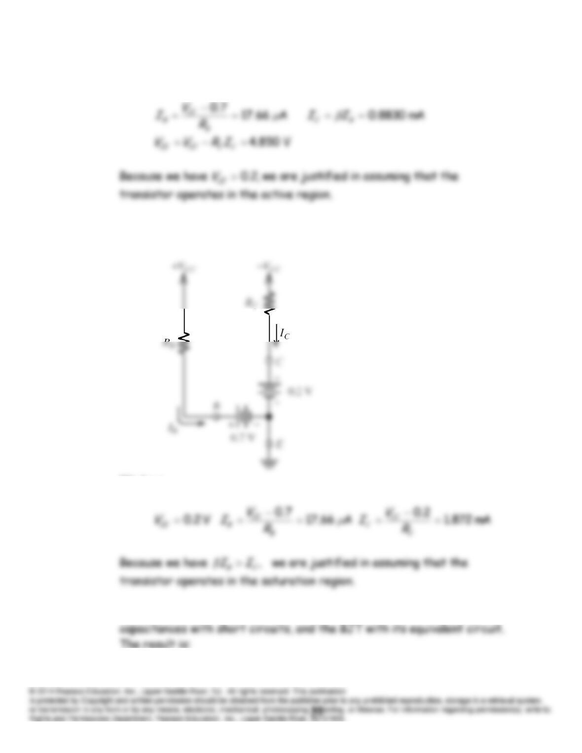
in which we have
VCC
9 V,
RC
4.7 k, and
RB
470 k.
We have
(b) In this case (
),250
the BJT operates in the saturation region.
The equivalent circuit is:
We have
T13.5 We need to replace
VCC
by a short circuit to ground, the coupling
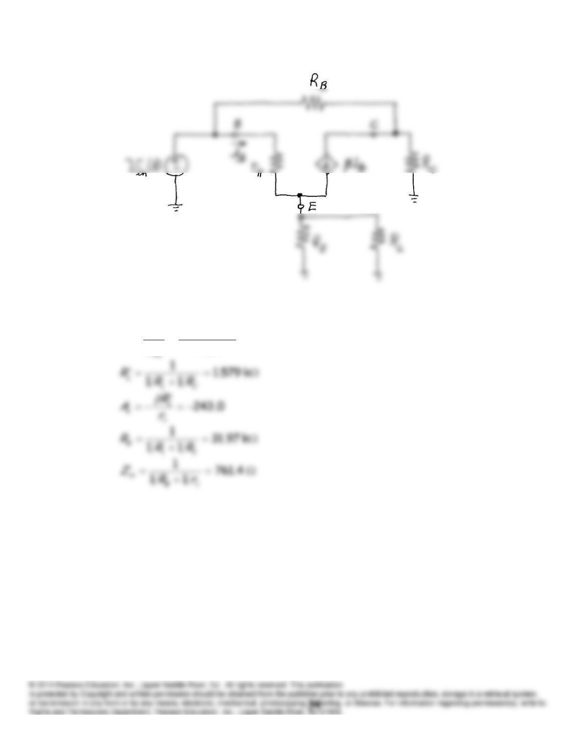
T13.6 This problem is similar to parts of Example 13.8.
780
mA 4
mV 26120
CQ
T
I
V
r