CHAPTER 12
Exercises
E12.1 (a)
vGS
1 V and
vDS
5 V: Because we have
vGS
<
Vto
, the FET is in
cutoff.
E12.2 First we notice that for
V, 1 or 0
GS
v
the transistor is in cutoff, and the
drain current is zero. Next we compute the drain current in the
The boundary between the triode and saturation regions occurs at
E12.3 First we notice that for
V, 1 or 0
GS
v
the transistor is in cutoff, and
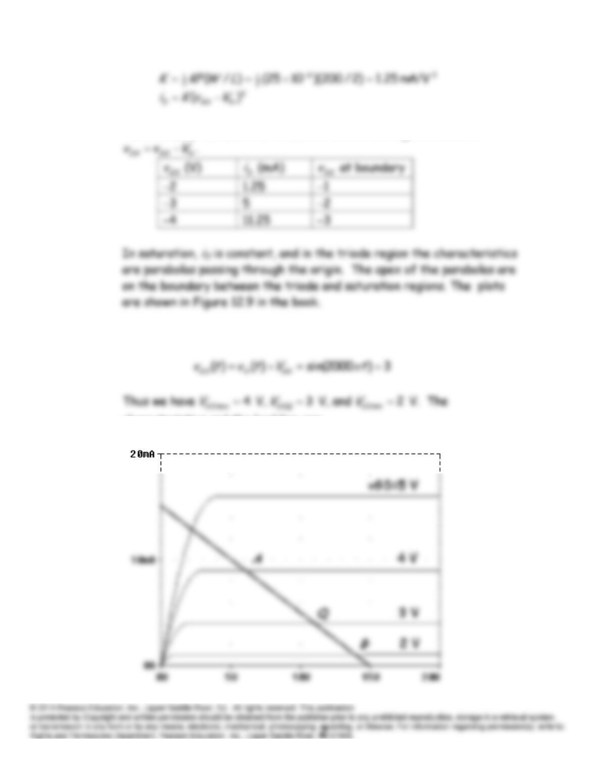
The boundary between the triode and saturation regions occurs at
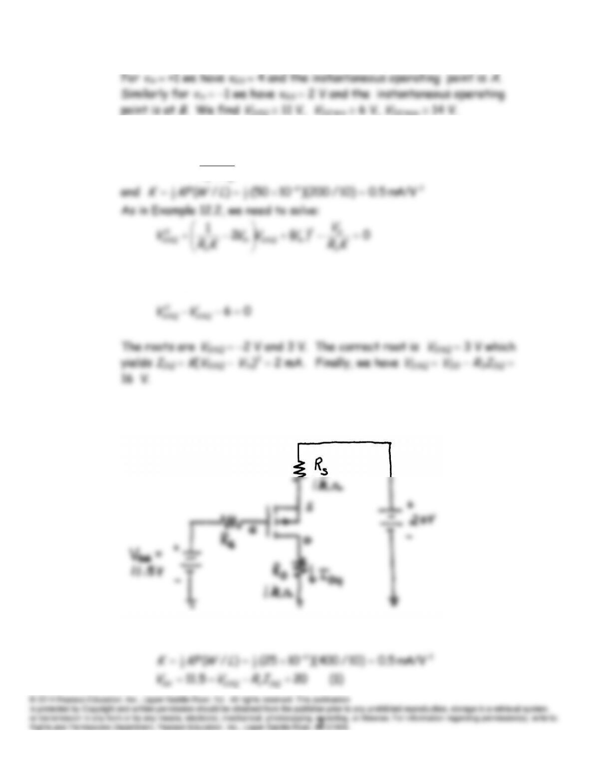
E12.4 We have
characteristics and the load line are:
E12.5 First, we compute
V 7
2
RR
R
VV DDG
Substituting values, we have
E12.6 First, we replace the gate bias circuit with its equivalent circuit:
Then we can write the following equations:
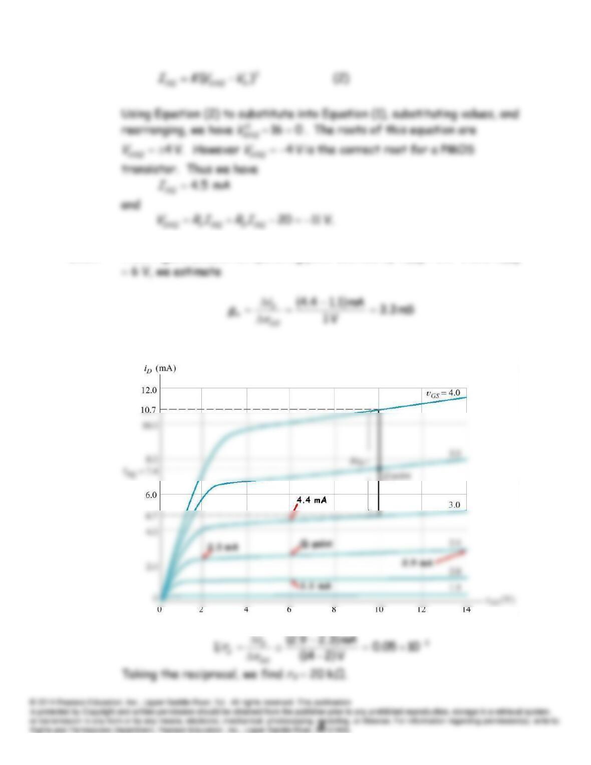
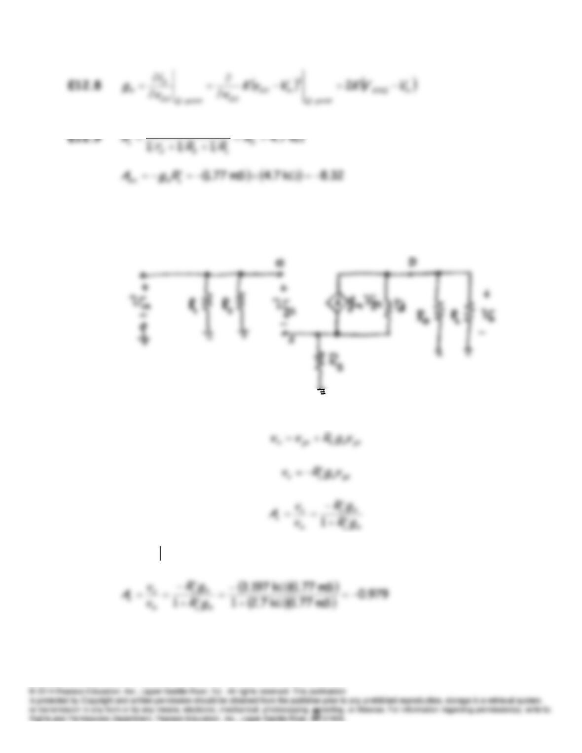
E12.7 From Figure 12.21 at an operating point defined by V
GSQ
2.5 V and V
DSQ
1
E12.10 For simplicity we treat
rd
as an open circuit and let
L
R
RD
RL
.
E12.11
Ωk 197.3
LDL RRR
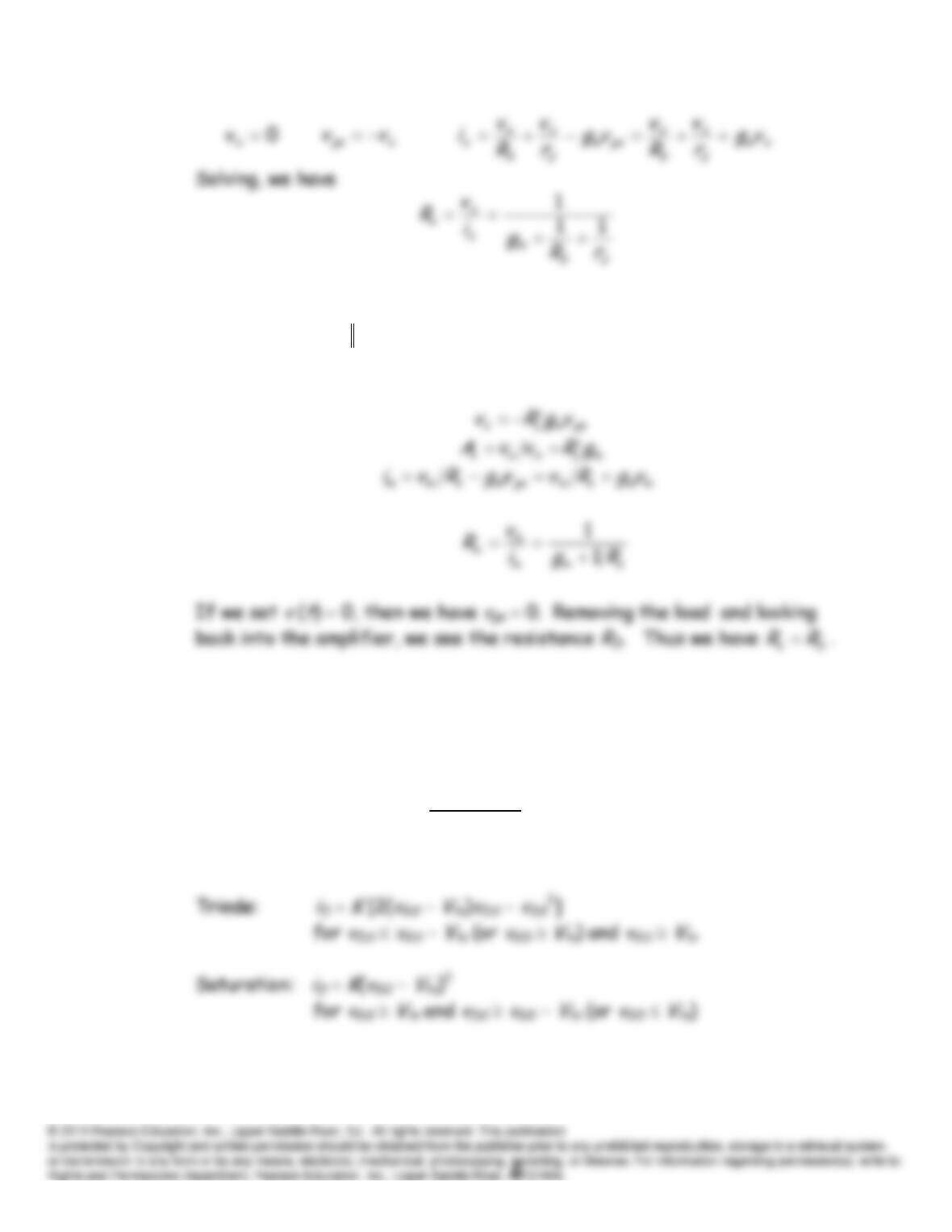
E12.12 The equivalent circuit is shown in Figure 12.28 in the book from which we
can write
E12.13 Refer to the small-signal equivalent circuit shown in Figure 12.30 in the
book. Let
LDL RRR
.
gs
vv
in
E12.14 See Figure 12.34 in the book.
E12.15 See Figure 12.35 in the book.
Problems
P12.1 Cutoff:
iD
0 for
vGS
Vto
P12.2 See Figures 12.1 and 12.2 in the book.
P12.3*
2
2
1mA/V 25.0)/(
LWKPK
P12.4*
iD
P12.5 We have
V. 5.0 for 0
GSDvi
Therefore, we have
V. 5.0
to
V
In the
P12.6 (a) Cutoff because we have
vGS
Vto
.
P12.7 The device is in saturation for
vDS
vGS
Vto
2 V. The device is in the
P12.8 With the gate connected to the drain, we have
vDS
vGS
so
vDS
vGS
Vto
.
P12.9 (a) This NMOS transistor is operating in saturation because we have
vGS
P12.10
2
2
1mA/V 5.0)/(
LWKPK
V 5
2
R
vGS
V 5
DS
v
P12.11
2
2
1mA/V 25.0)/(
LWKPK
V 5
1
RR
R
vGS
V 5
DS
v
P12.12* In the saturation region, we have
iD
K
(
vGS
Vto
)2. Substituting values,
we obtain two equations:
Dividing each side of the second equation by the respective side of the
first, we obtain
P12.13* We have
2
)(
to
GSDVvKi
. Substituting values and solving, we obtain
P12.14 With
vGS
vDS
5 V, the transistor operates in the saturation region for
P12.15 To obtain the least drain current choose minimum
W
and maximum
L
(i.e.,
2/
2)/(
1/
1) 64.
P12.16 For a device operating in the triode region, we have
Then, the resistance between drain and source is given by
With the device in cutoff (i.e.,
vGS
Vto
), the drain current is zero and
rd
is infinite. Evaluating, we have:
vGS
(V)
rd
(kΩ)
P12.17 (a) This is an NMOS transistor. We have
vGS
v
in and
vDS
5 V. With
v
in
P12.18 Because
vGD
4 5 1 V is less than
Vto
, the transistor is operating in
P12.19 Distortion occurs in FET amplifiers because of curvature and nonuniform
spacing of the characteristic curves.
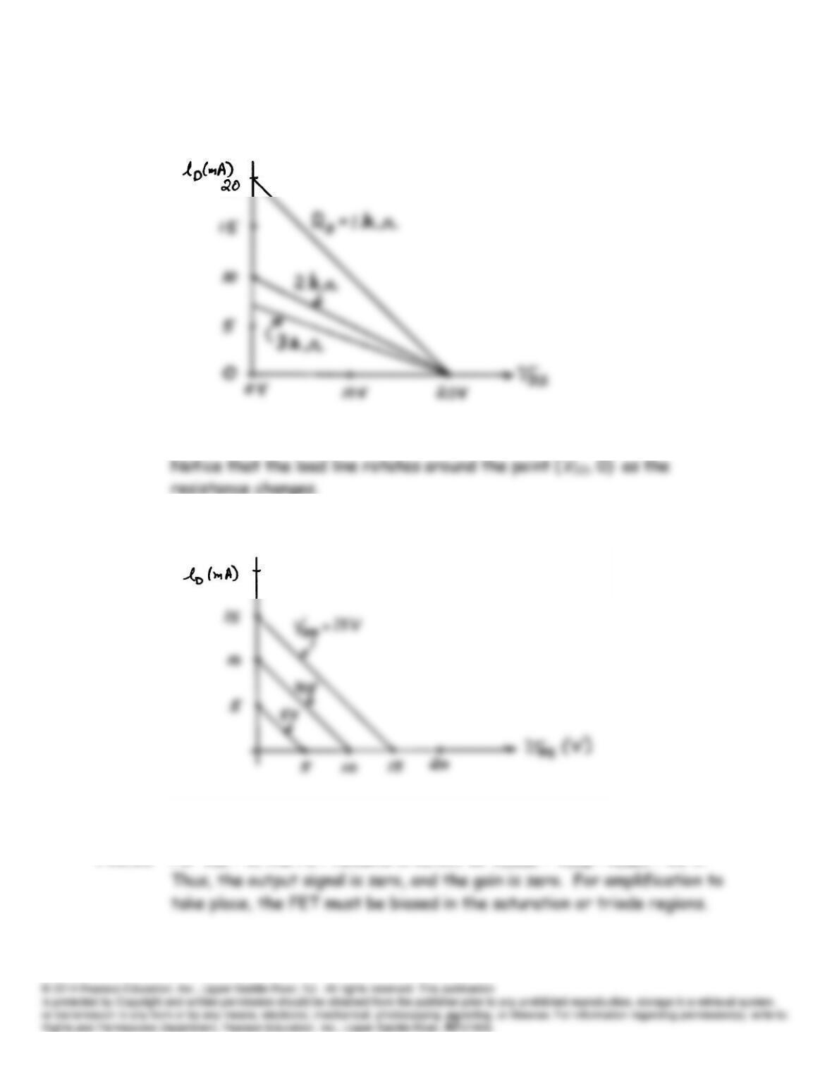
P12.20* The load-line equation is
VDD
RDiD
+
vDS
, and the plots are:
P12.21 The load-line equation is
VDD
RDiD
+
vDS
, and the plots are:
Notice that the load lines are parallel as long as
RD
is constant.
P12.22* For
VGG
0, the FET remains in cutoff so
VDS
VDSQ
VDS
P12.23 (a) The 1625 kΩ and 375 kΩ resistors act as a voltage divider that
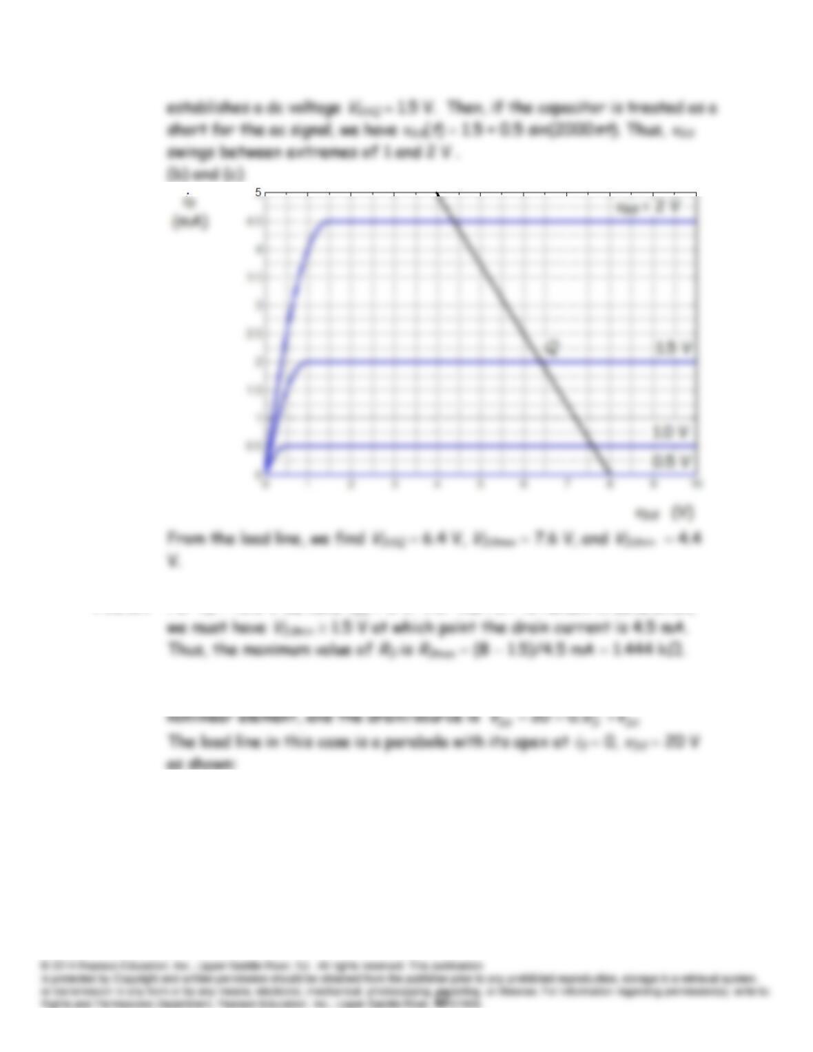
P12.24 For
vin
+0.5 V we have
vGS
2 V. For the FET to remain in saturation,
P12.25 The KVL equation around the loop consisting of the
VDD
source, the
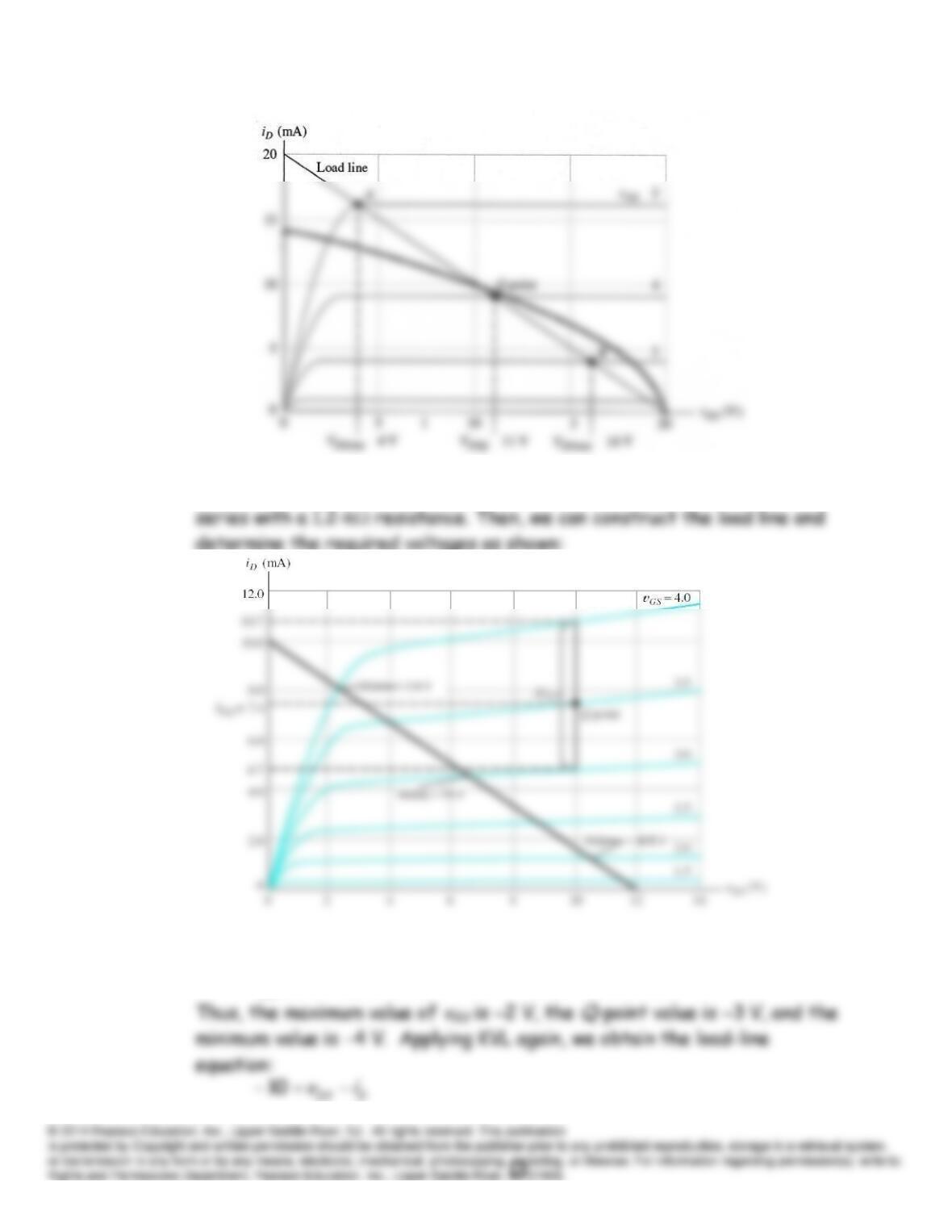
P12.26 The Thévenin equivalent for the drain circuit contains a 12-V source in
P12.27 Using KVL, we have
)2000sin(3107)2000sin()(
tttvGS
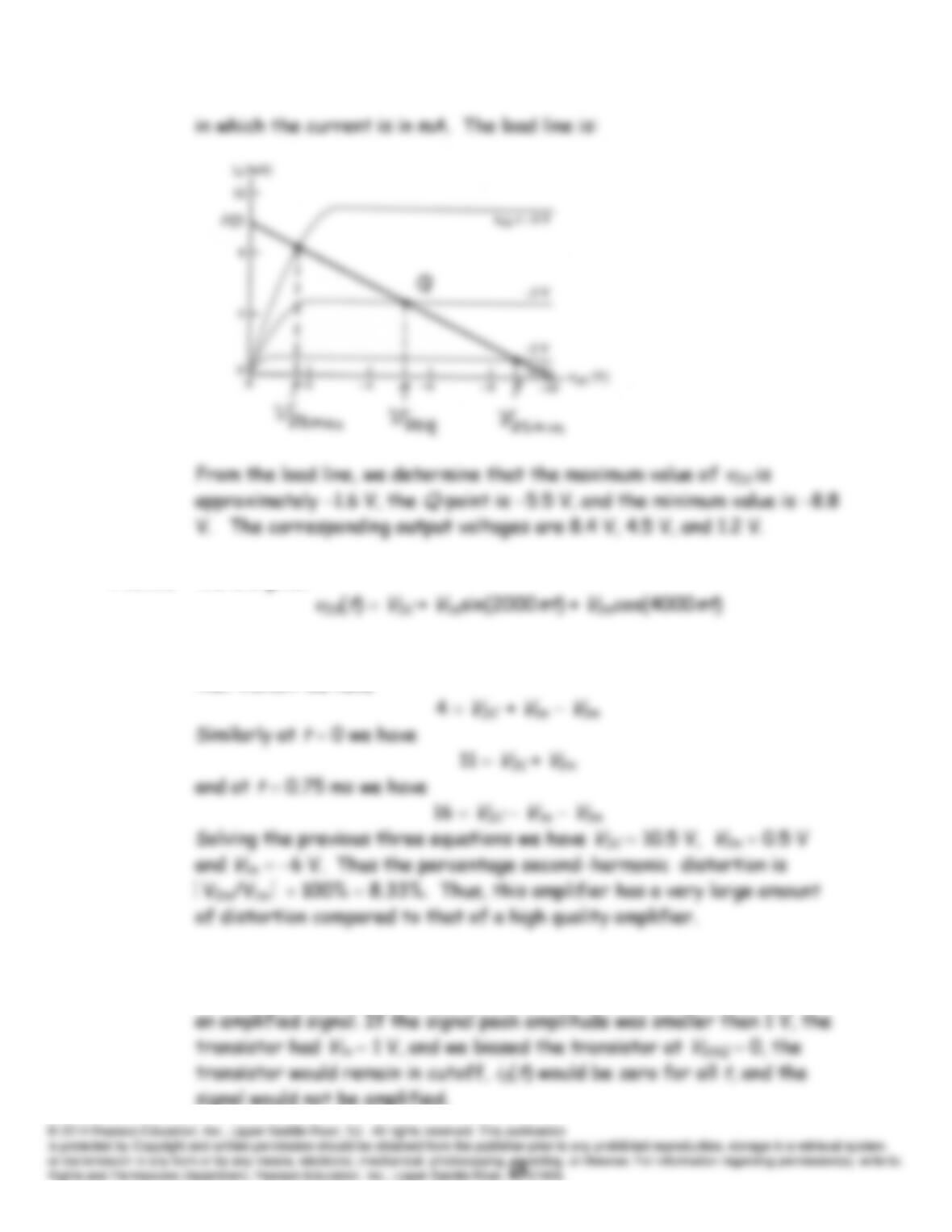
P12.28 We are given
Evaluating at
t
0.25 ms and observing that the plot gives
vDS
4 V at
that instant we have
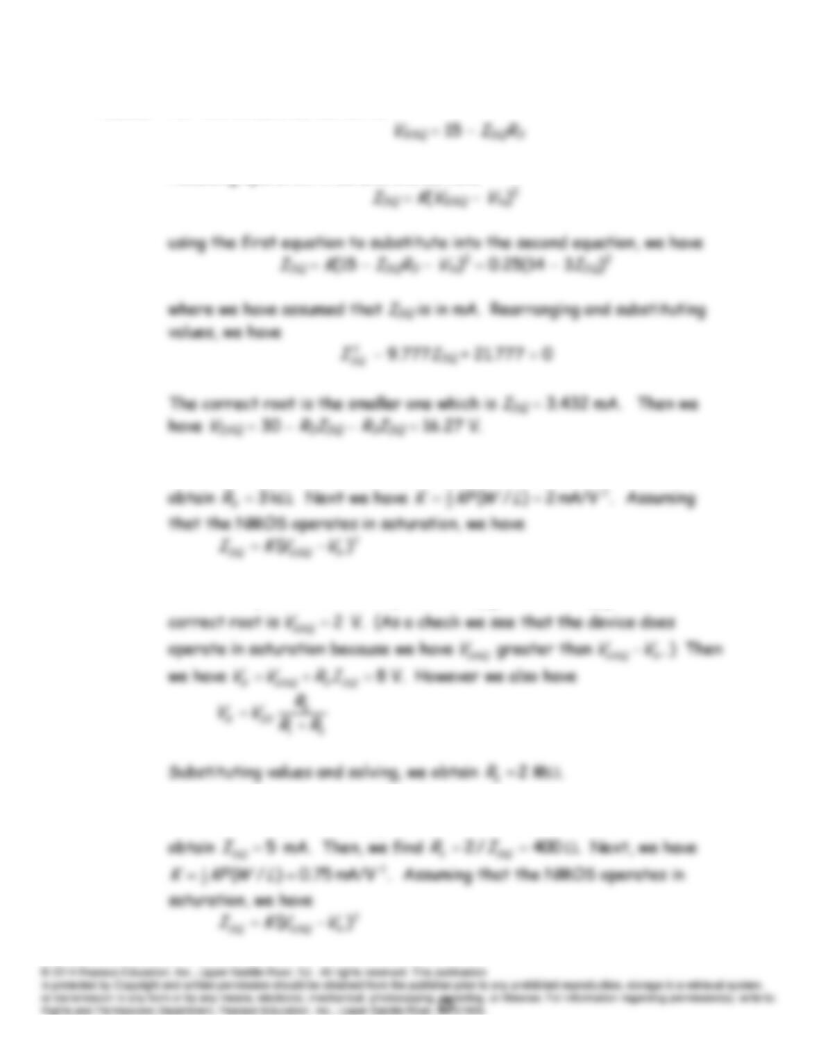
P12.29 In an amplifier circuit, we need to bias the MOSFET so the ac signal to
be amplified can cause changes in the currents and voltages resulting in
P12.30* For this circuit, we can write
Assuming operation in saturation, we have
P12.31* We can write
DQ
S
DSQDD IRVV
. Substituting values and solving, we
Substituting values and solving, we find
0
GSQ
V
V and
2
GSQ
V
V. The
2
GSQ
V
P12.32* We can write
28220
DQDD IV
in which
IDQ
is in mA. Solving, we