Substituting values and solving we find
582.1
GSQ
V
V and
582.3
GSQ
V
P12.34* We have
VGSQ
VDSQ
VDD
RDIDQ
. Then substituting
IDQ
K
(
VGSQ
Vto
)2, we have
P12.35 First, we use Equation 12.11 to compute
As in Example 12.2, we need to solve:
Substituting values, we have
P12.36 Assuming that the MOSFET is in saturation, we have
where we have assumed that
IDQ
and
K
are in mA and mA/V2
respectively. Using the second equation to substitute in the first,
substituting values and rearranging, we have
P12.37 We can write
DQ
S
DSQDQDDD IRVIRV
. Substituting values and solving
Substituting values and solving we find
1
GSQ
V
V and
0.3
GSQ
V
V. The
0.3
GSQ
V
P12.38 Because
vGD
1 is zero, the first transistor operates in saturation. We have
Substituting values and solving, we find
0.1
GSQ
V
V and
3
GSQ
V
V.
3
GSQ
V
i
i
P12.42 From Figure P12.42 at an operating point defined by
VGSQ
2.5 V and
VDSQ
6 V, we have
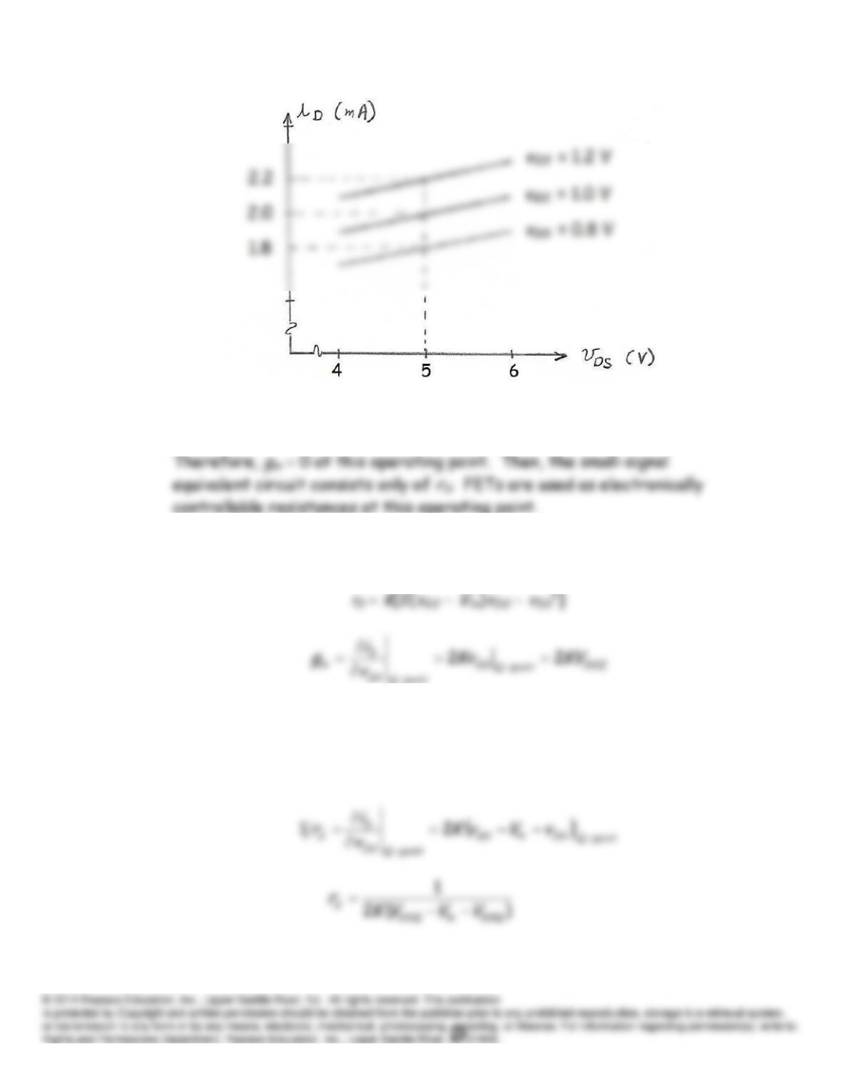
P12.43 We will sketch the characteristics for
vGS
ranging a few tenths of a volt
on either side of the
Q
point.
gm
determines the spacing between the
The sketch of the curves is:
P12.44 For
VDSQ
0, the vertical spacing of the drain characteristics is zero.
P12.45* In the triode region, we have
P12.46* In the triode region, we have
iD
K
[2(
vGS
Vto
)
vDS
vDS
2]
P12.47
mS 168 point
D
i
g
P12.48
mS 718.2)1exp()exp( point
GS
D
mv
i
g
P12.49 This transistor is operating with constant
vGS
. Thus, we can determine
rd
by dividing the peak ac drain-to-source voltage by the peak ac drain
current.
P12.50 This transistor is operating with constant
vDS
. Thus, we can determine
gm
P12.51 See Figure 12.22 in the book.
P12.52 Coupling capacitors act as open circuits for dc and as approximate short
P12.53* (a)
V 3
3.07.1
3.0
20
2
RR
R
VV DDG
(b)
Ω 500
1
LRR
R
P12.54 (a)
V 3
3.07.1
3.0
20
2
RR
R
VV DDG
(b)
Ω 500
1
R
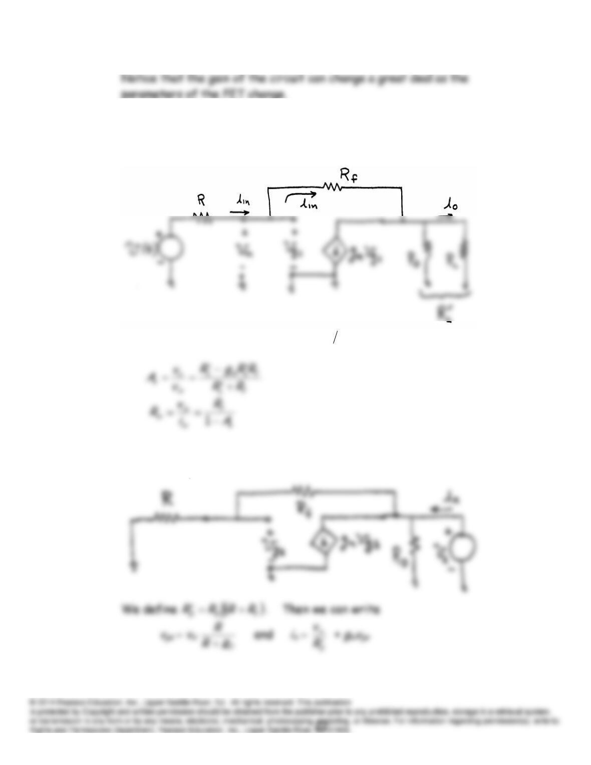
P12.55 (a)
(b)
f
o
ininin
m
in
L
oRvvivgiRv
The circuit used to determine output impedance is:
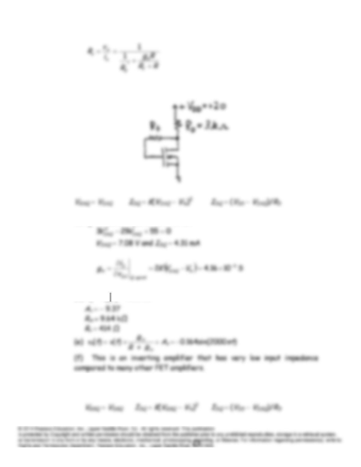
(c) The dc circuit is:
Using the above equations, we obtain
(d)
Ωk 31.2
LDL RRR
P12.56* Referring to the circuit shown in Figure P12.56, we have
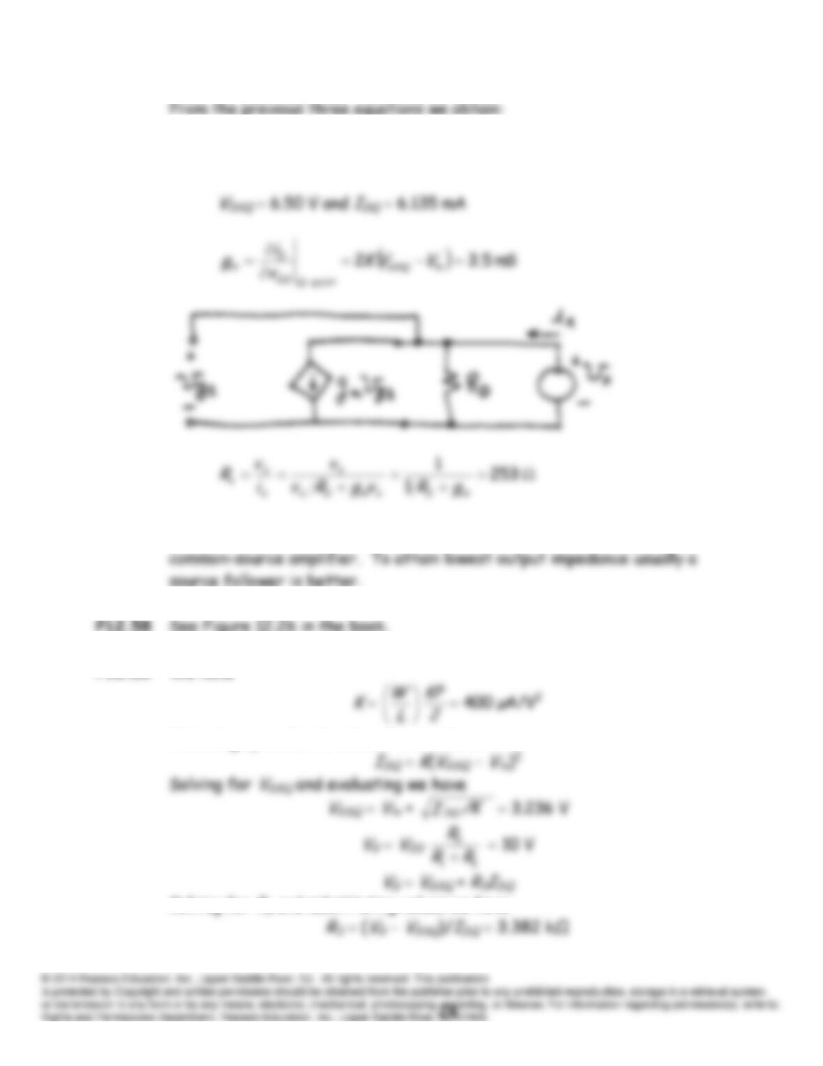
01.106.51.1 2
DSQDSQ VV
P12.57 If we need a voltage-gain magnitude greater than unity, we choose a
P12.59* We have
Assuming operation in saturation, we have
Solving for
RS
and substituting values we have
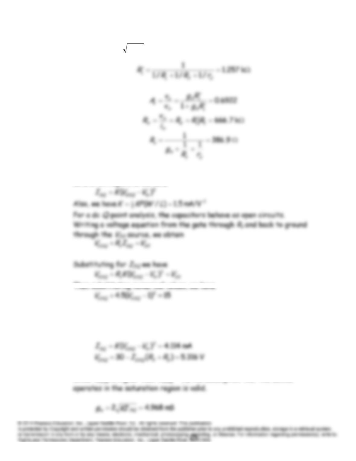
We have
gm
2
KI DQ
1.789 mS
P12.60 (a) We start by assuming that the MOSFET is operating in the
saturation region, so we have
Solving, we obtain
VGSQ
2.656 V (The other root is extraneous.) Then
we have
Since
VDSQ
is higher than
VGSQ Vto
the assumption that the device
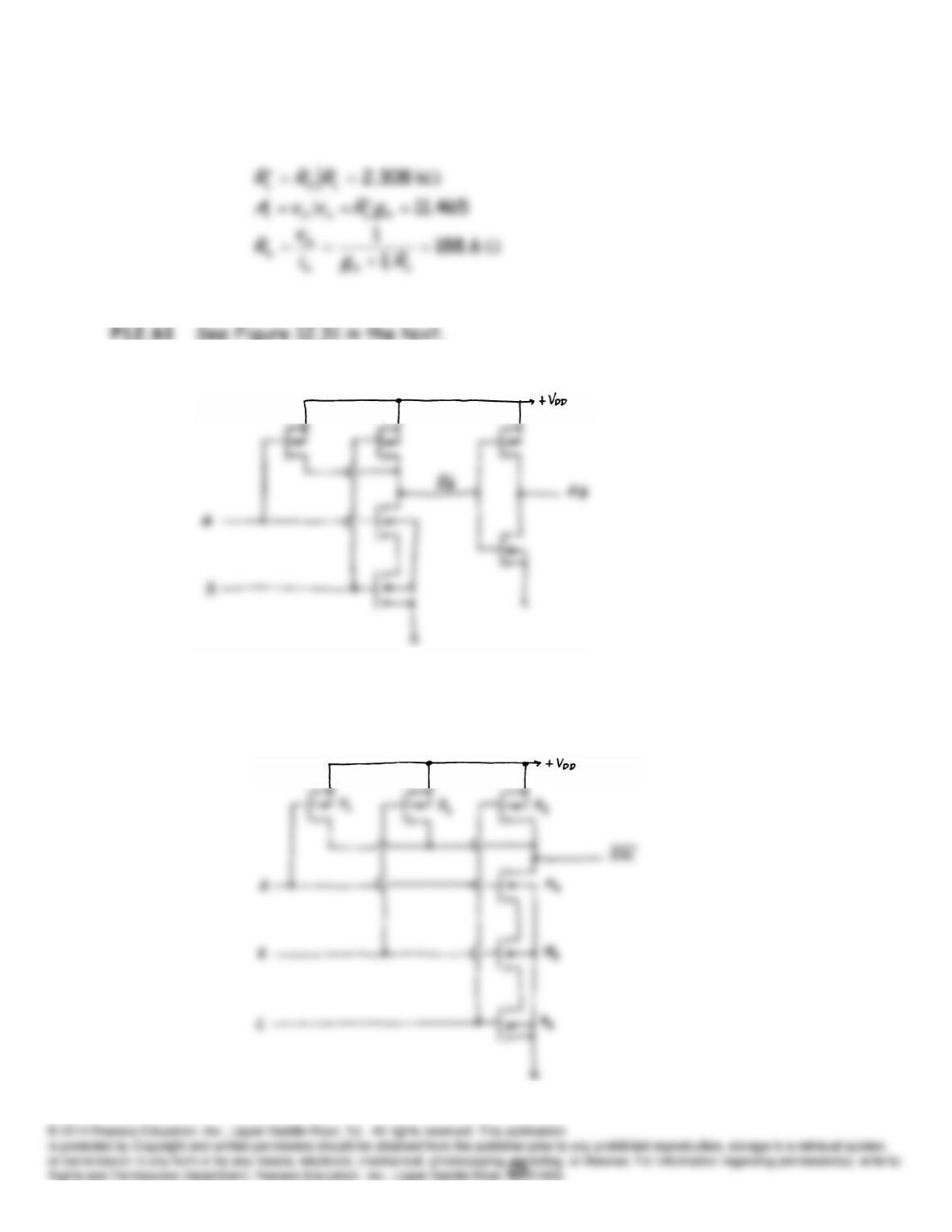
(b) Using the results from Exercise 12.13, we have
P12.62
P12.63 (a)
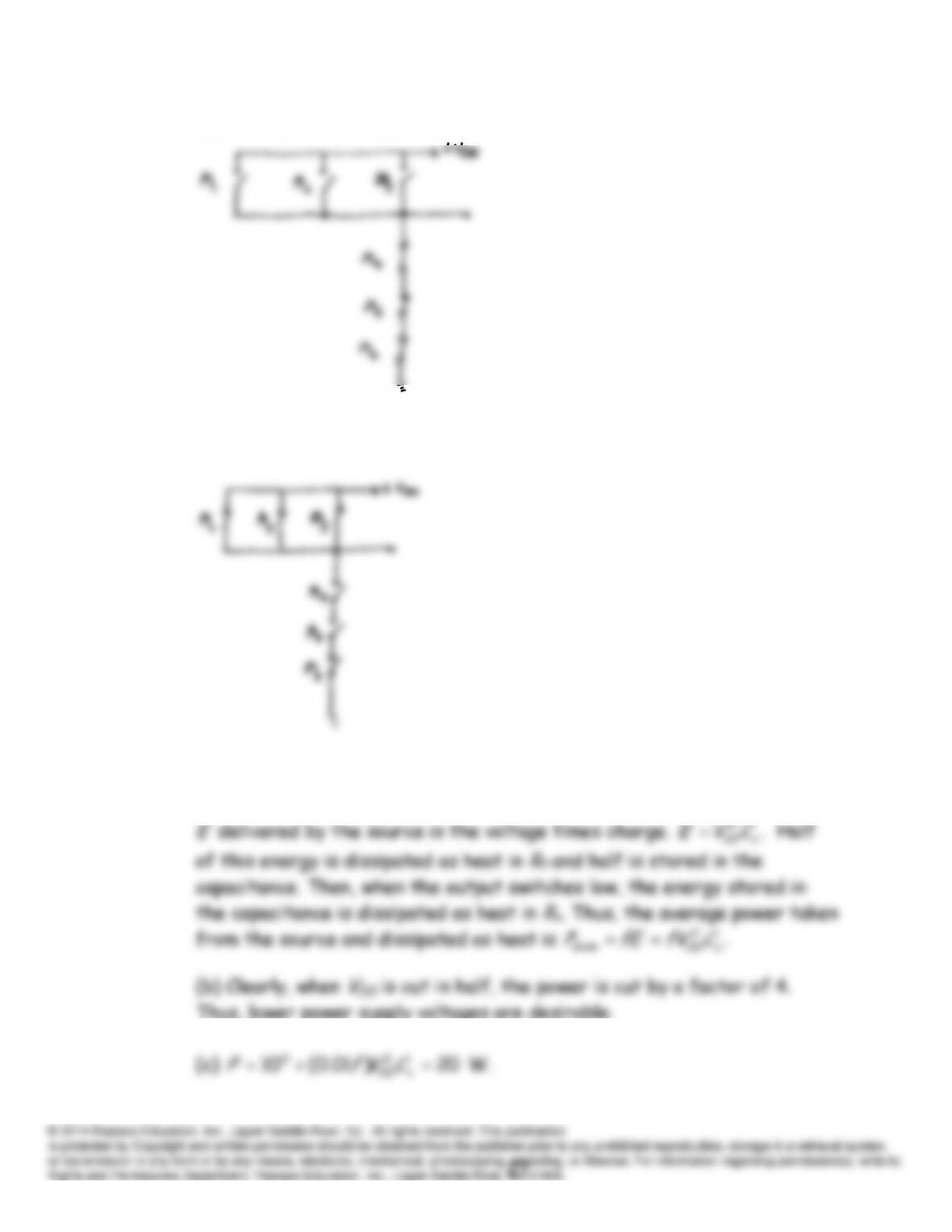
(b) All inputs high:
(c) All inputs low:
P12.64 (a) The charge flowing from the source to charge the load capacitance
each time the output switches from low to high is
.
LDDCVQ
The energy
Practice Test
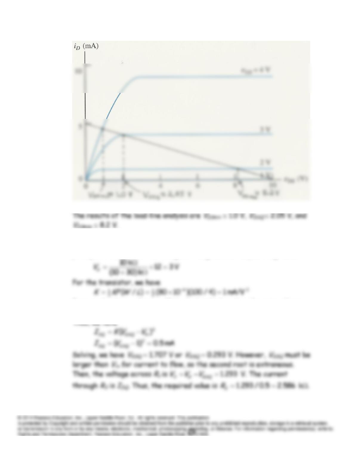
T12.1 Drain characteristics are plots of
iD
versus
vDS
for various values of
vGS
.
First, we notice that for
V, 5.0
GS
v
the transistor is in cutoff, and the
Next, we compute the drain current in the saturation region for
V. 4
v
T12.2 We have
3)2000sin()()(
tVtvtv GG
in
GS
V. Thus, we have
4
max
GS
V
T12.3 Because the gate current is zero, we can apply the voltage division
principle to determine the voltage at the gate with respect to ground.
Because the drain voltage is 12 V, which is higher than the gate voltage,
we conclude that the transistor is operating in the saturation region.
T12.4 This transistor is operating with constant
vDS
. Thus, we can determine
gm
by dividing the peak ac drain current by the peak ac gate-to-source
voltage.
T12.5 (a) A dc voltage source is replaced with a short circuit in the small-signal
T12.6 See Figure 12.31(b) and (c) in the text.