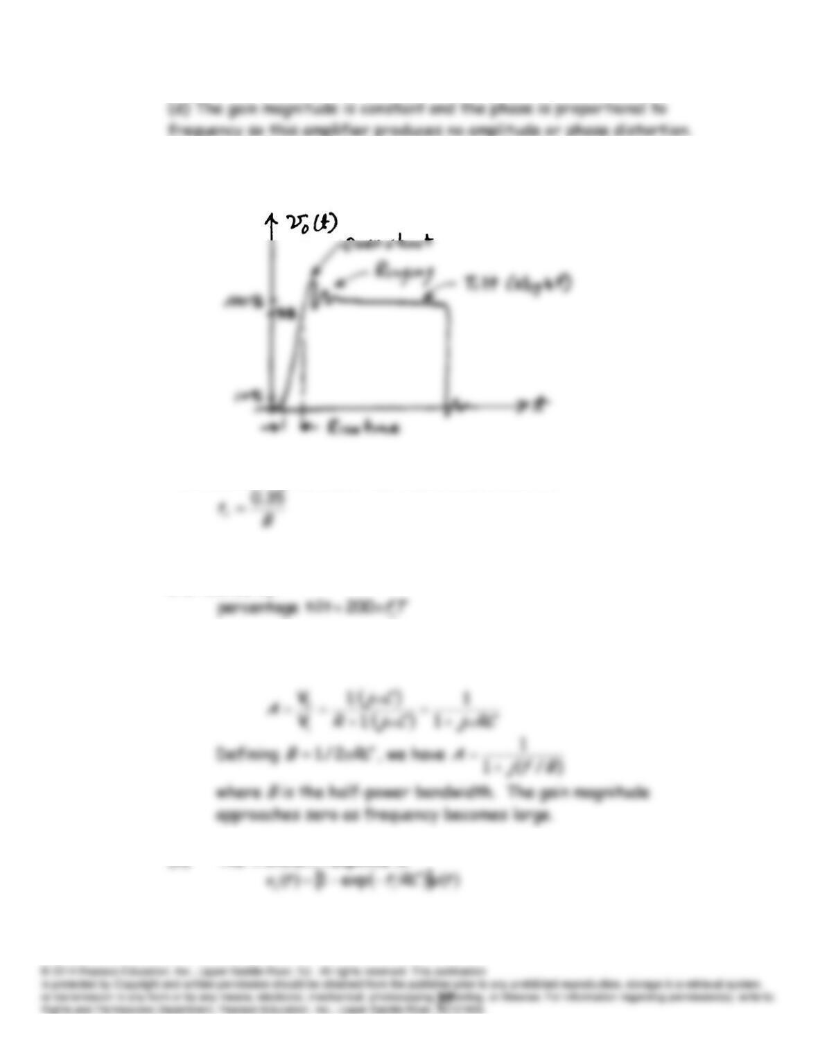
P11.79 The sketch is
The relationship between rise time and bandwidth is:
Percentage tilt, the lower half-power frequency, and the pulse duration
are related by:
P11.80 (a) Applying the voltage-division principle, we have
(b) The transient response is:
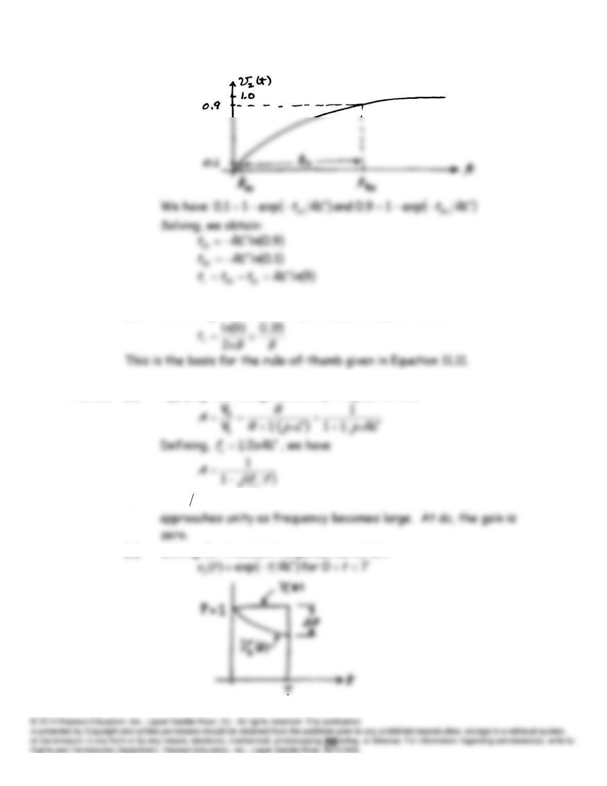
(c) Combining the results of parts (a) and (b), we obtain
P11.81 (a) Applying the voltage-division principle, we have
RCfL
π21
(b)
RCfL
π21
is the half-power frequency. The gain magnitude
(c) Solving for transient response, we obtain:
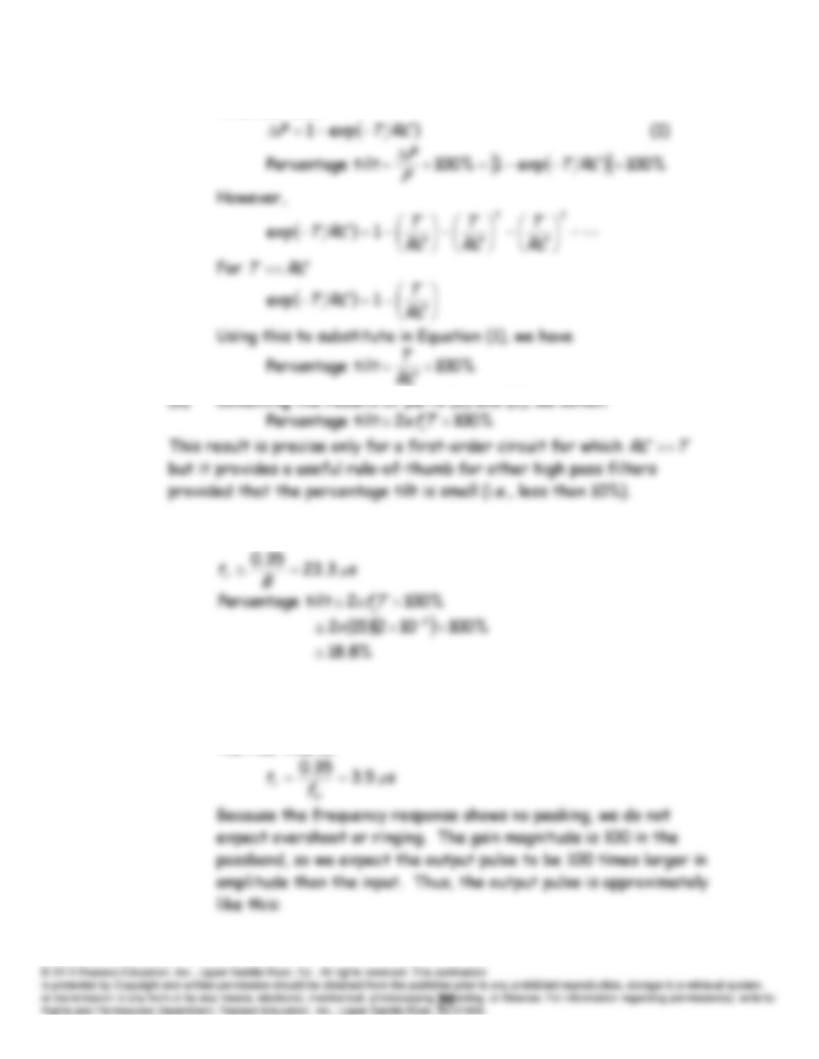
Thus, we have:
P11.82*
kHz 15
H
fB
P11.83* (a) Because the amplifier is dc-coupled (i.e.,
0
L
f
), the tilt is zero.
The upper half-power frequency is
kHz 100
H
f
, and we estimate
the rise time as
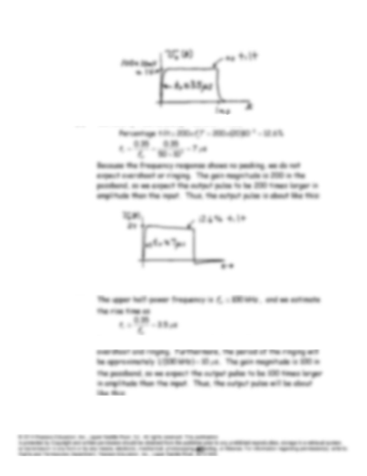
(b) We have
kHz 50 and Hz 20
. Thus,
(c) Because the amplifier is dc-coupled (i.e.,
0
L
f
), the tilt is zero.
Because the frequency response displays peaking, we expect
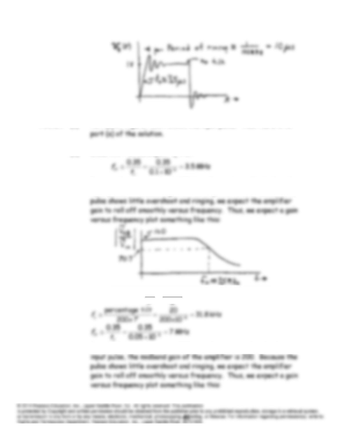
P11.84 (a) Part (a) of Figure P11.84 shows the input pulse. Thus there is no
(b) Since
0
tilt
, we expect
0
f
.
Because the output pulse is 100 times larger in amplitude than the
input pulse, the midband gain of the amplifier is 100. Because the
(c)
%20
6.12
tilt Percentage
P
Because the output pulse is 200 times larger in amplitude than the
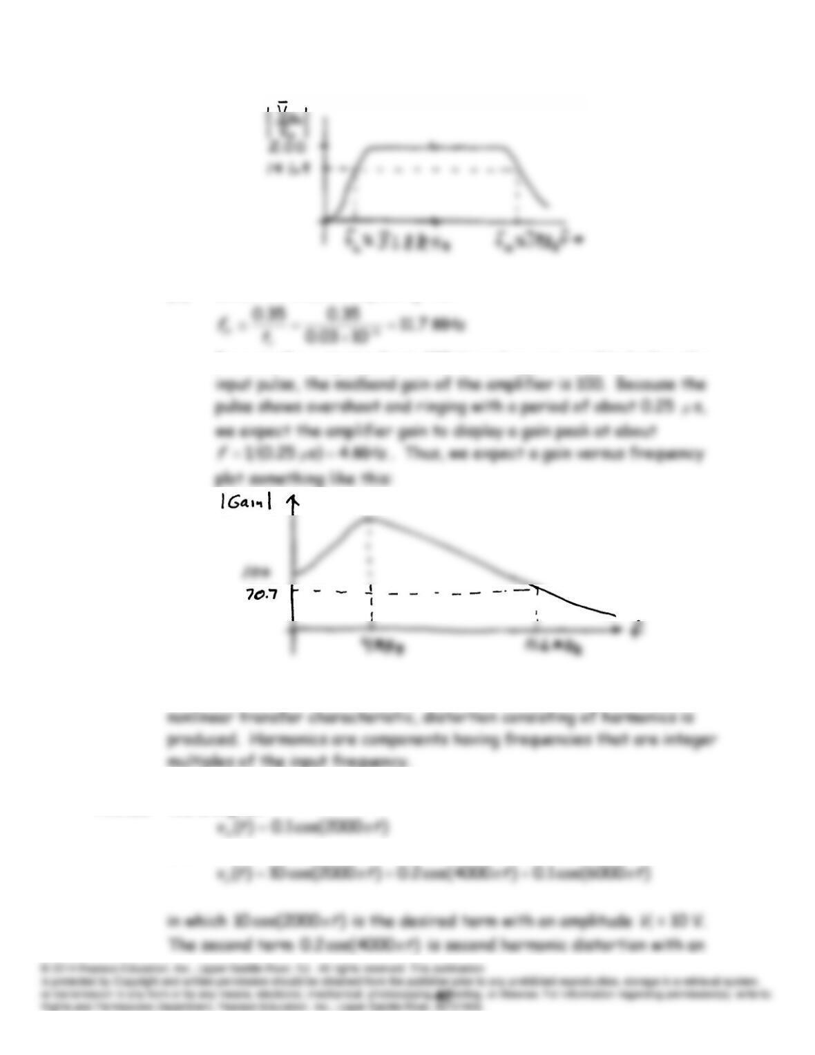
(d) Since
0 tilt
, we expect
0
L
f
.
Because the output pulse in 100 times larger in amplitude than the
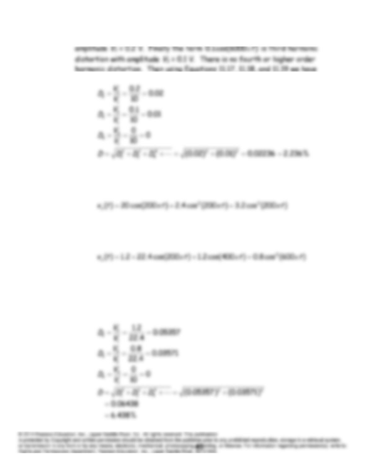
P11.85 When a sinewave input signal is passed through an amplifier having a
P11.86* We are given
and
P11.87 Substituting the input into the equation for the transfer characteristic,
we obtain:
Applying the trigonometric identities suggested in the problem
statement, we obtain
Thus, the amplitude of the desired output term is
V
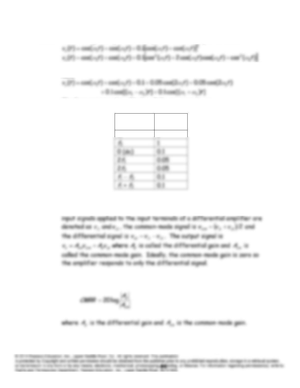
1 = 22.4, the
amplitude of the second harmonic is
V
2 = 1.2 V, and the amplitude of the
third harmonic is
V
3 = 0.8 V. The amplitudes of higher order terms are
zero. Then using Equations 11.17, 11.18, and 11.19, we have
P11.88 Substituting the input into the equation for the output we obtain
Next, applying the identities suggested in the problem and simplifying, we
have
The frequencies and amplitudes of the components are:
Frequency
(Hz)
Amplitude
(V)
0 (dc)
0.1
2
0.05
f
0.1
f
1
P11.89 A differential amplifier has two input terminals, one is known as the
inverting input and the other is known as the noninverting input. If the
P11.90 The common-mode rejection ratio (in decibels) is defined as
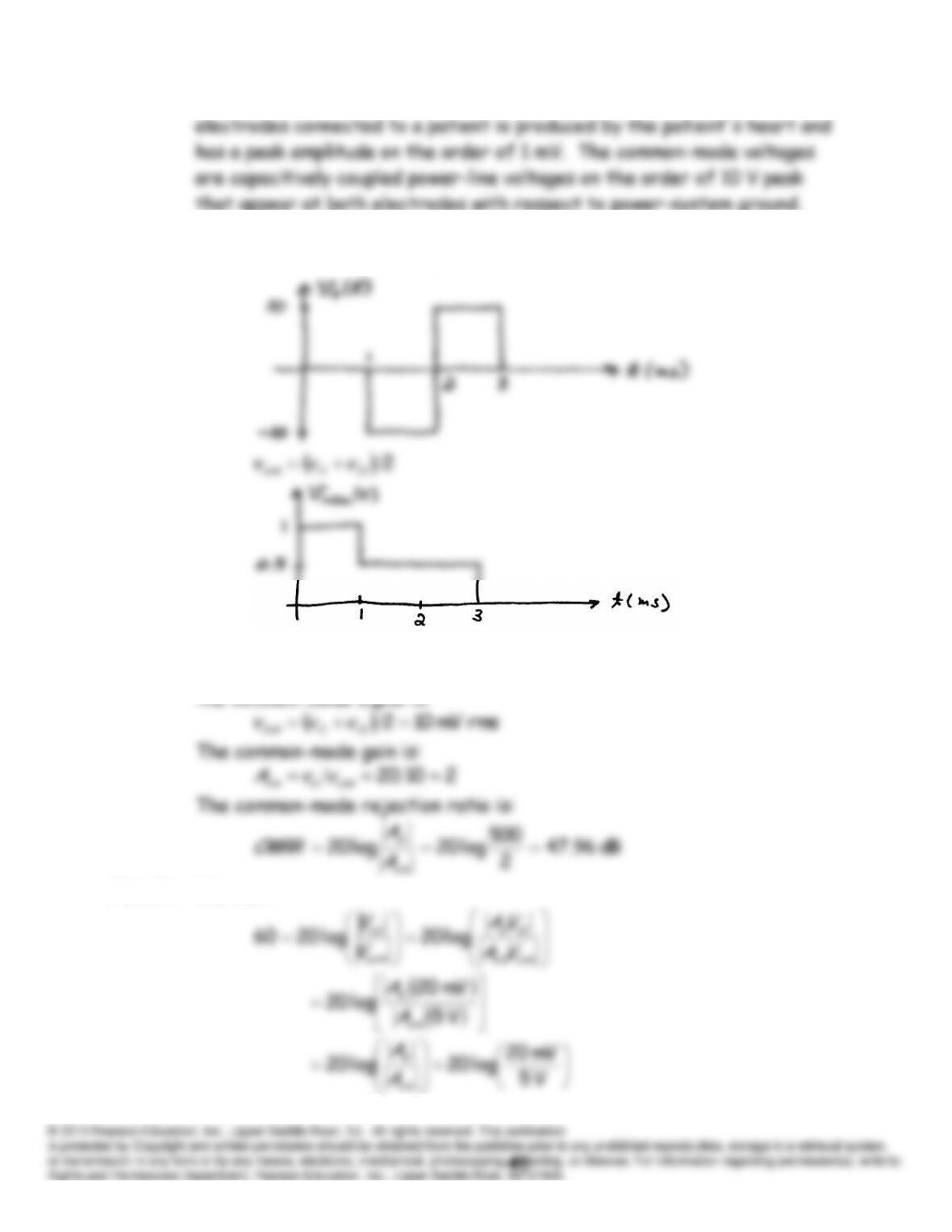
P11.91 Electrocardiography provides a classic example of differential and
common-mode signals. The differential signal between a pair of
P11.92
21
10
ii
idd
ovvvAv
P11.93* With the input terminals tied together, the differential signal is zero and
P11.94 We want
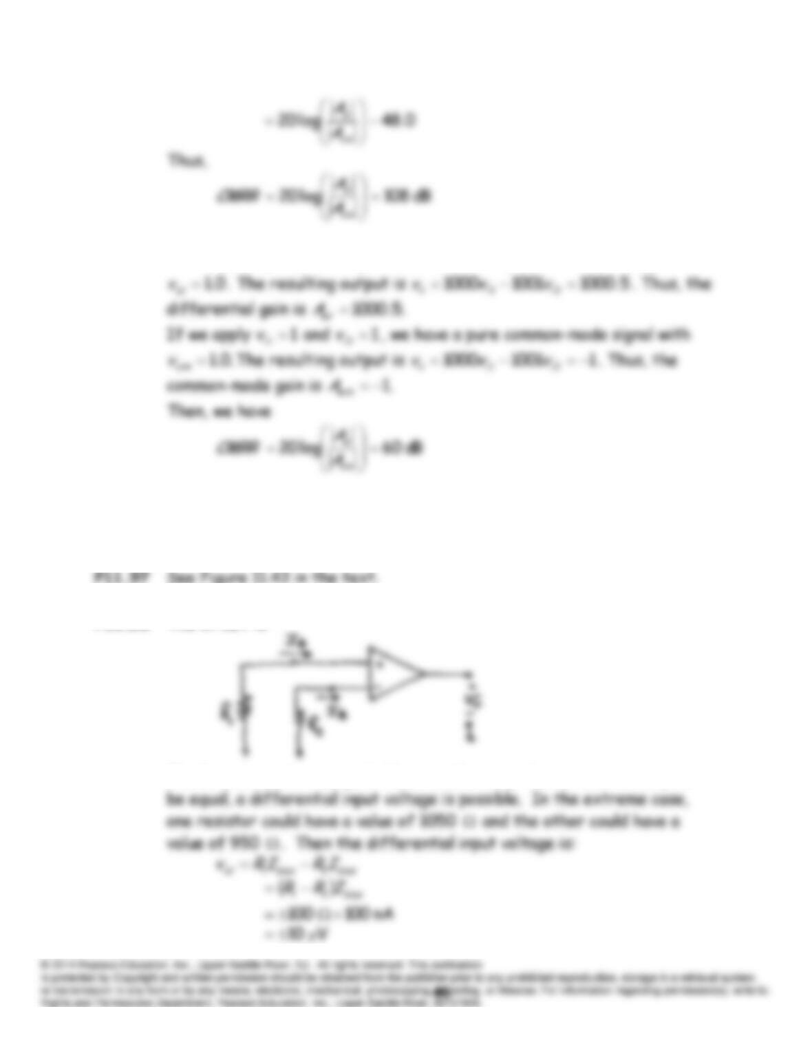
P11.95 If we apply
5.0
1
i
v
and
5.0
2
i
v
, we have a pure differential signal with
P11.96 See Figure 11.40 in the text. The effect of these sources is to add a dc
component to the output.
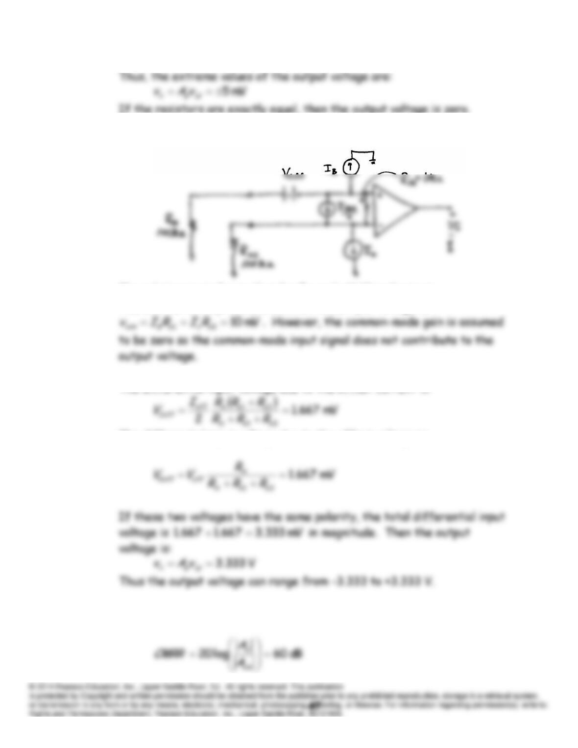
P11.98* The circuit is:
The bias currents are equal. However, because the resistances may not
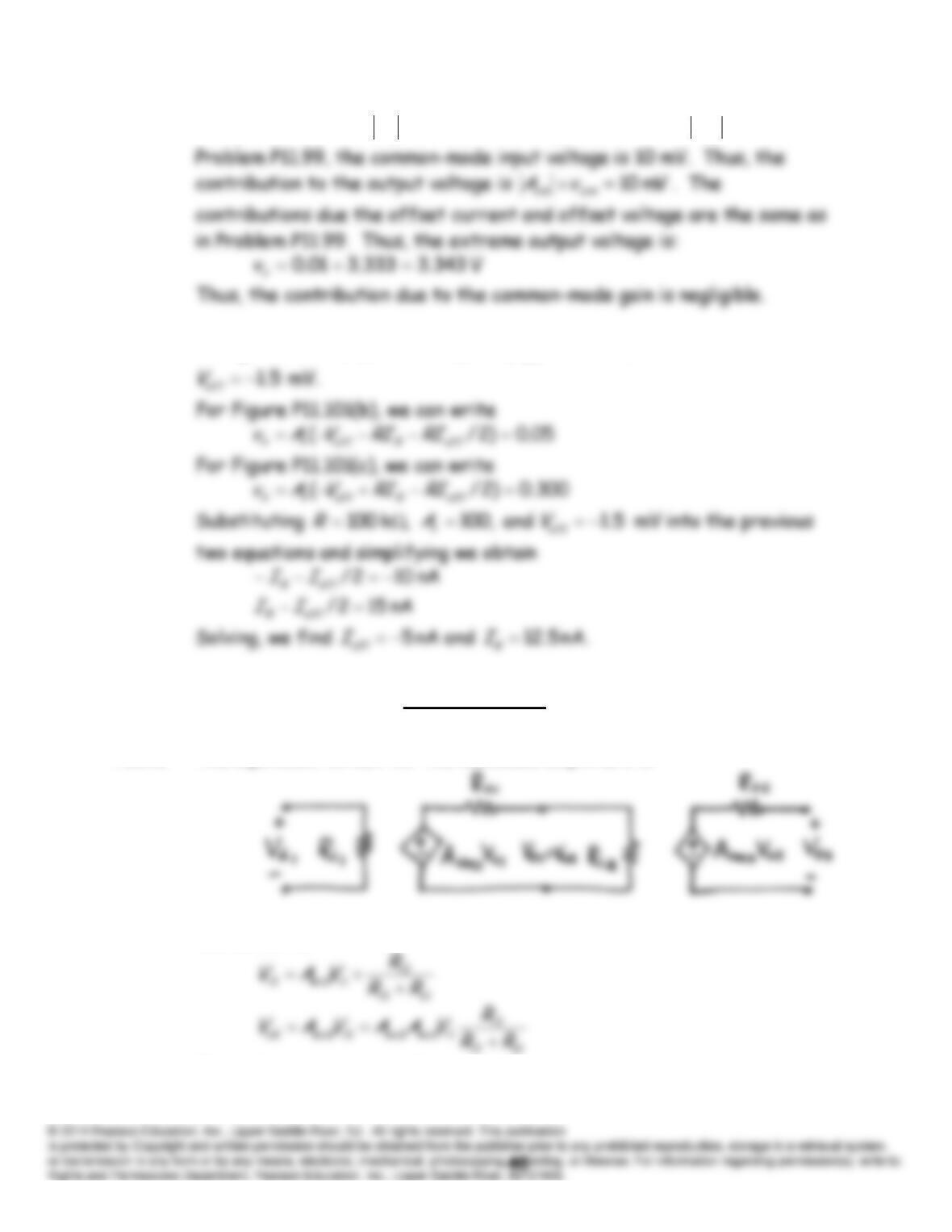
P11.99* The equivalent circuit is:
The solution is similar to that for Example 11.13 in the text.
The bias currents produce a common-mode input voltage of
The differential input voltage due to the offset current is:
The differential input voltage due to the offset voltage is:
P11.100 The common-mode rejection ratio is:
Using the fact that
1000
d
A
and solving, we find that
1
cm
A
. As in
P11.101 In Figure P11.101(a), we have
150
off
VAv vo
mV, from which we obtain
Practice Test
T11.1 The equivalent circuit for the cascaded amplifiers is:
We can write:
Thus, the open-circuit voltage gain is:
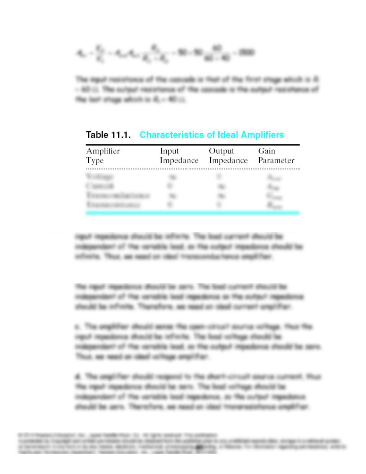
T11.2 Your answer should be similar to Table 11.1.
T11.3 a. The amplifier should sense the open-circuit source voltage, thus the
b. The amplifier should respond to the short-circuit source current, thus
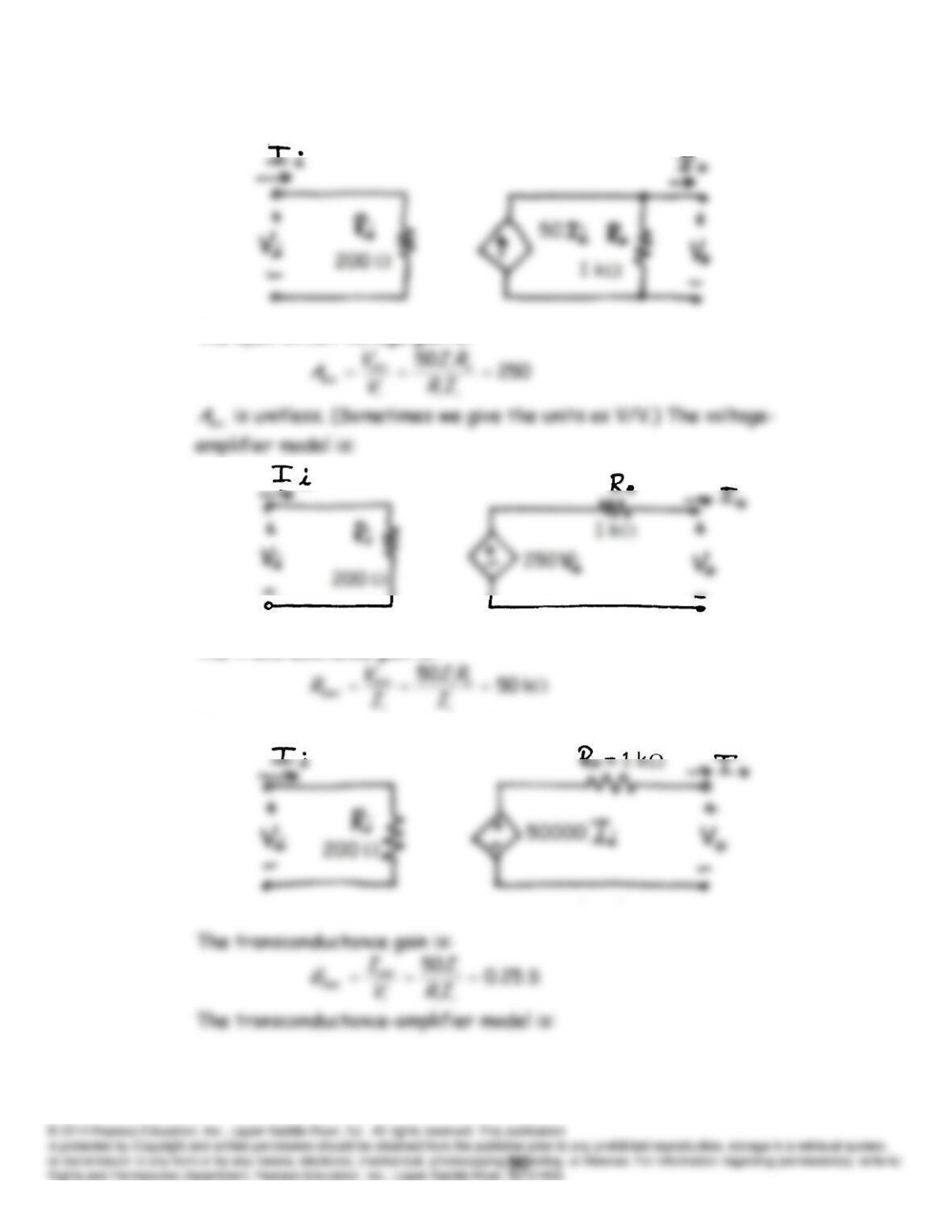
T11.4 We are given the parameters for the current-amplifier model, which is:
The open-circuit voltage gain is:
The transresistance gain is:
The transresistance-amplifier model is:
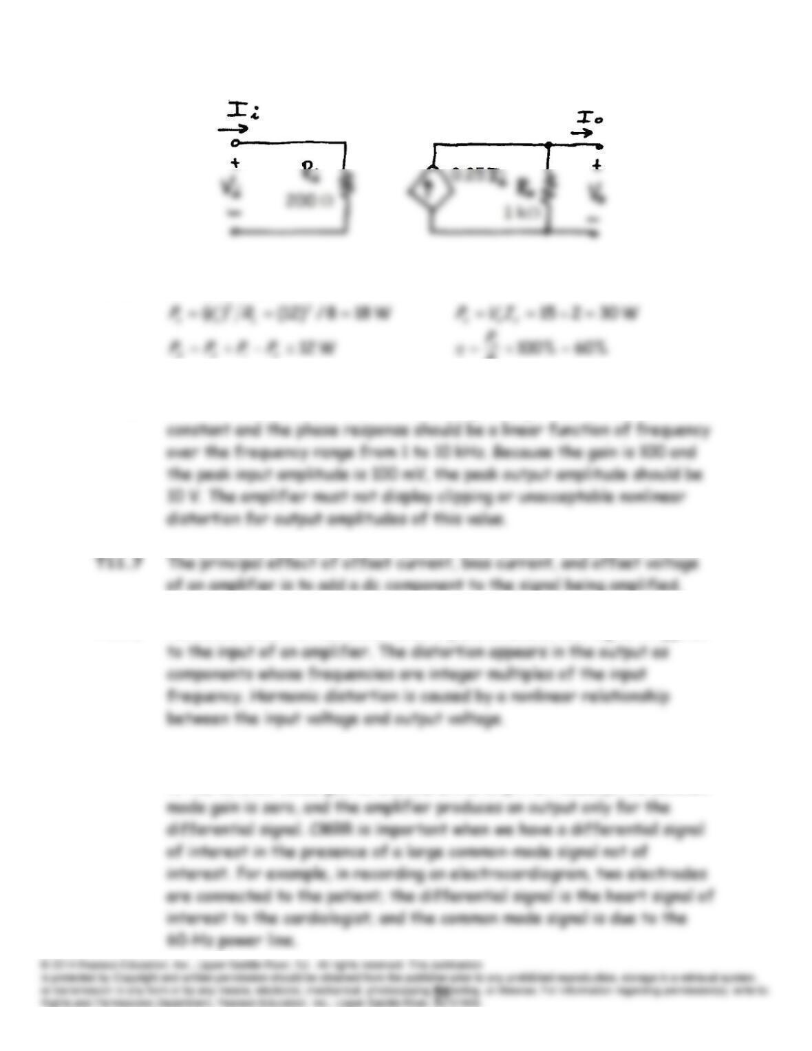
T11.5
mW 2102)10(3232
iii RIP
s
P
T11.6 To avoid linear waveform distortion, the gain magnitude should be
T11.8 Harmonic distortion can occur when a pure sinewave test signal is applied
T11.9 Common mode rejection ratio (CMRR) is the ratio of the differential gain
to the common mode gain of a differential amplifier. Ideally, the common