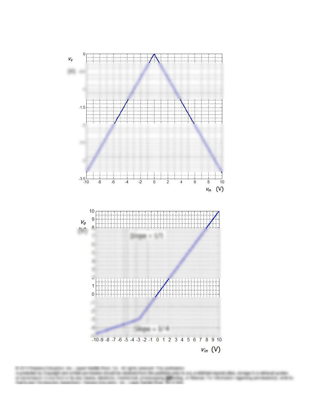
P10.65
P10.66
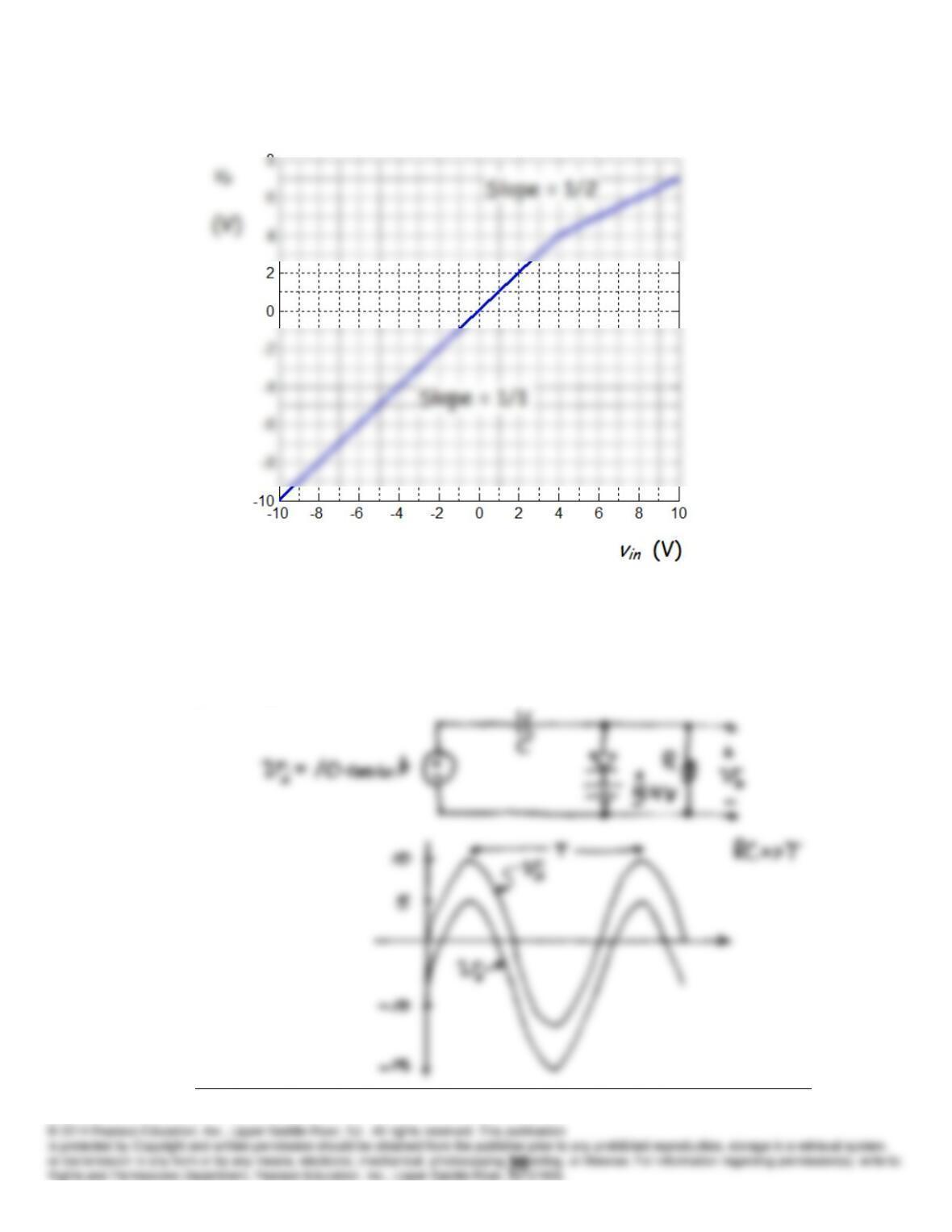
P10.67
P10.68 A clamp circuit adds or subtracts a dc component to the input waveform
such that either the positive peak or the negative peak is forced to
assume a predetermined value. An example circuit that clamps the
positive peak to +5 V is shown below:
We have allowed a forward drop of 0.6 V for the diode.
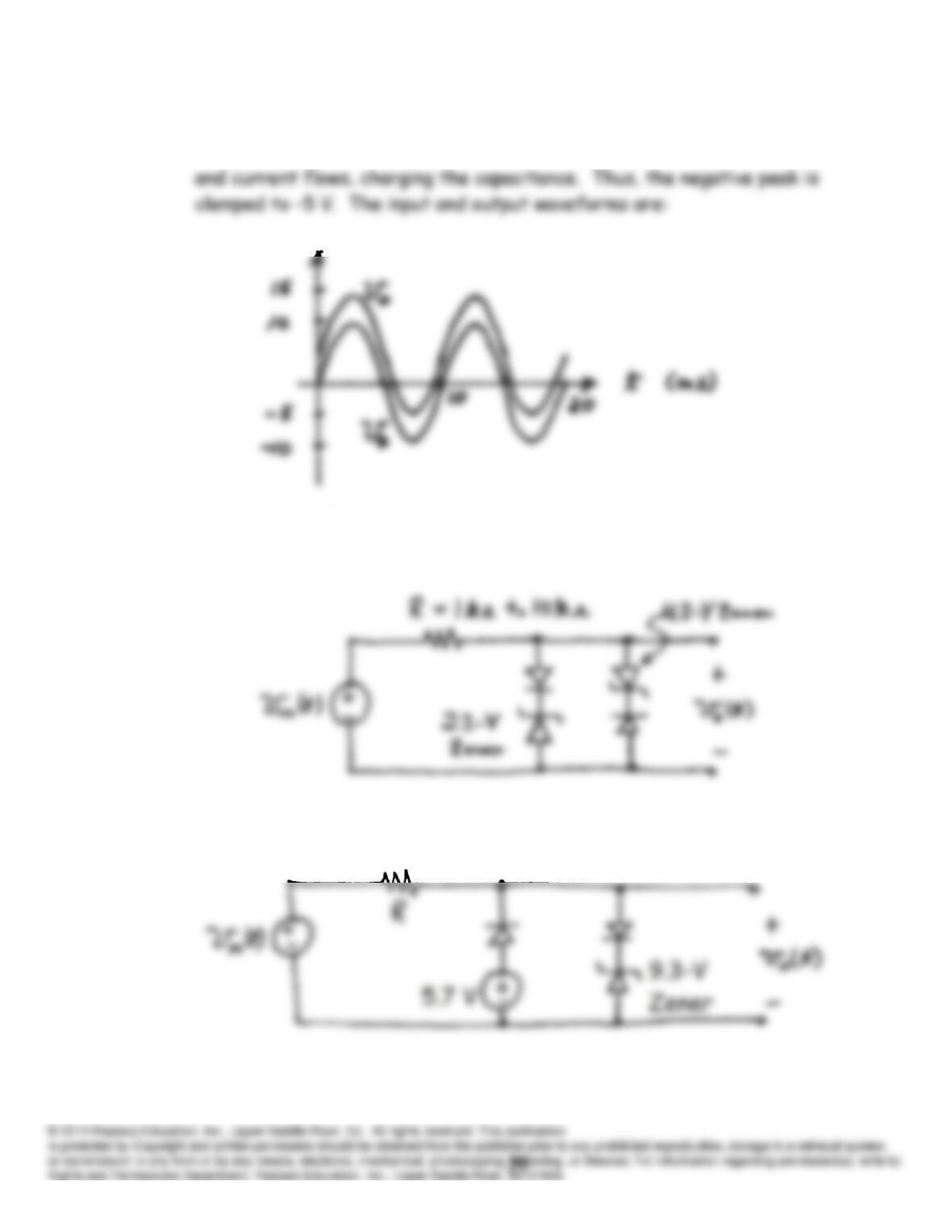
P10.69* Refer to the circuit shown in Figure P10.69 in the book. If the output
voltage attempts to become less than -5 V, the Zener diode breaks down
P10.70* A suitable circuit is:
P10.71 A suitable circuit is:
P10.72 This is a clamp circuit that clamps the positive peaks to zero.
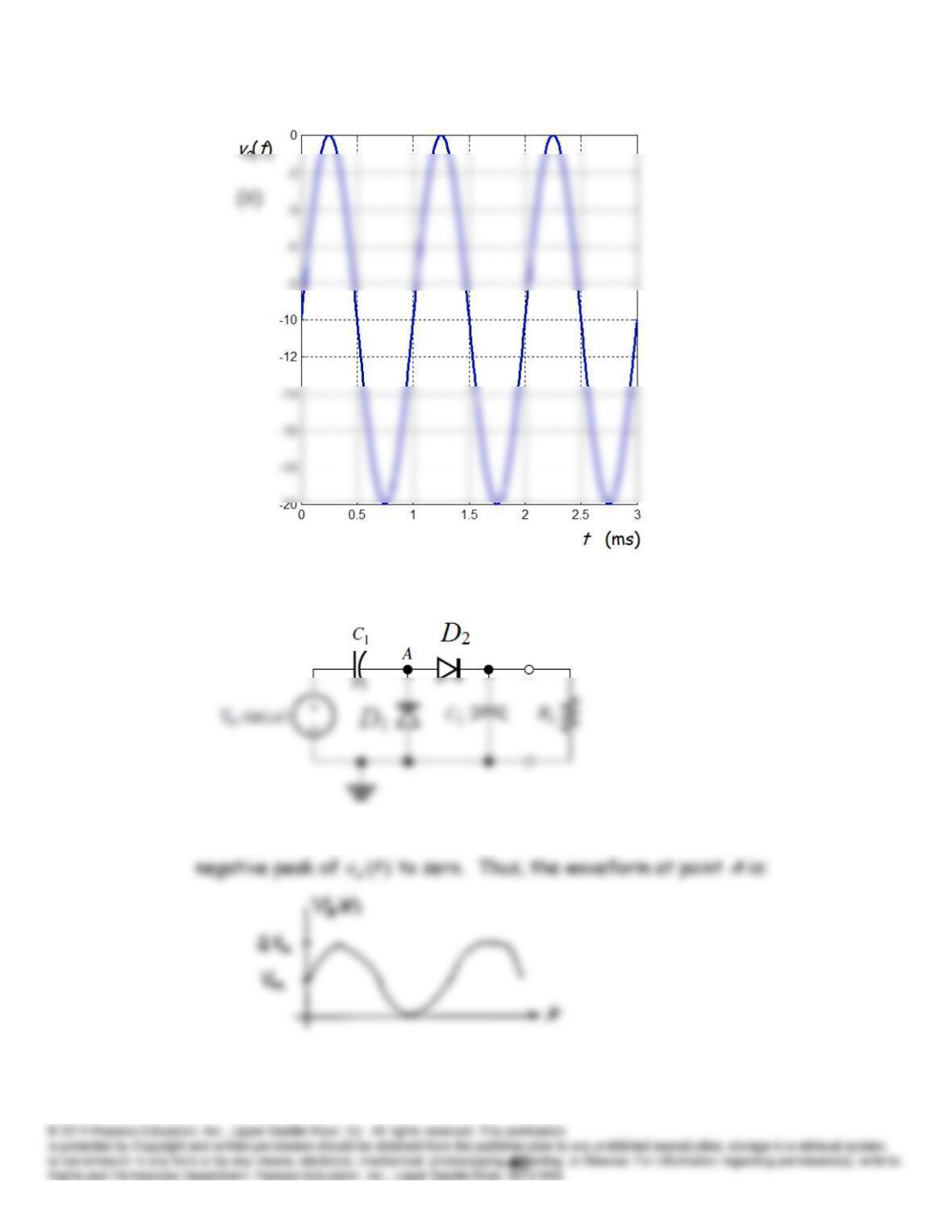
P10.73
The capacitor
1
C
and diode
1
D
act as a clamp circuit that clamps the
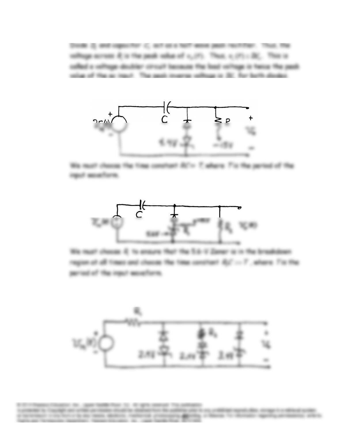
m
P10.74* A suitable circuit is:
P10.75 A suitable circuit is:
P10.76 (a) A suitable circuit is:
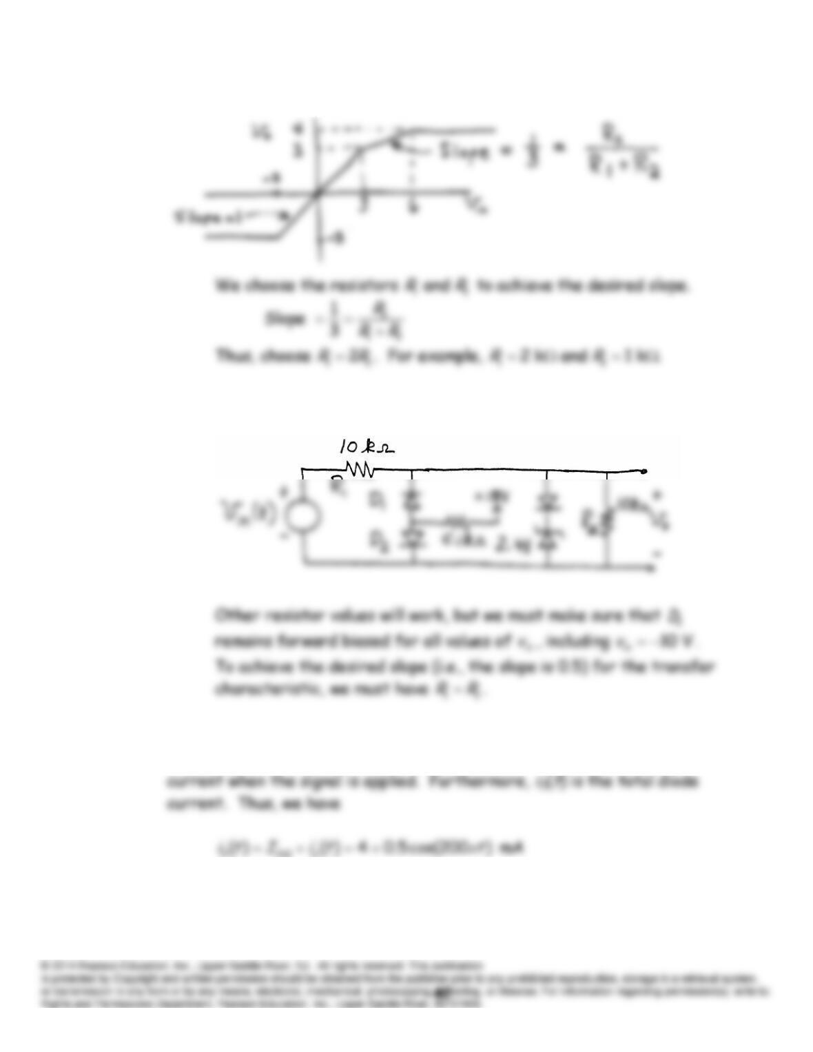
(b) A suitable circuit is:
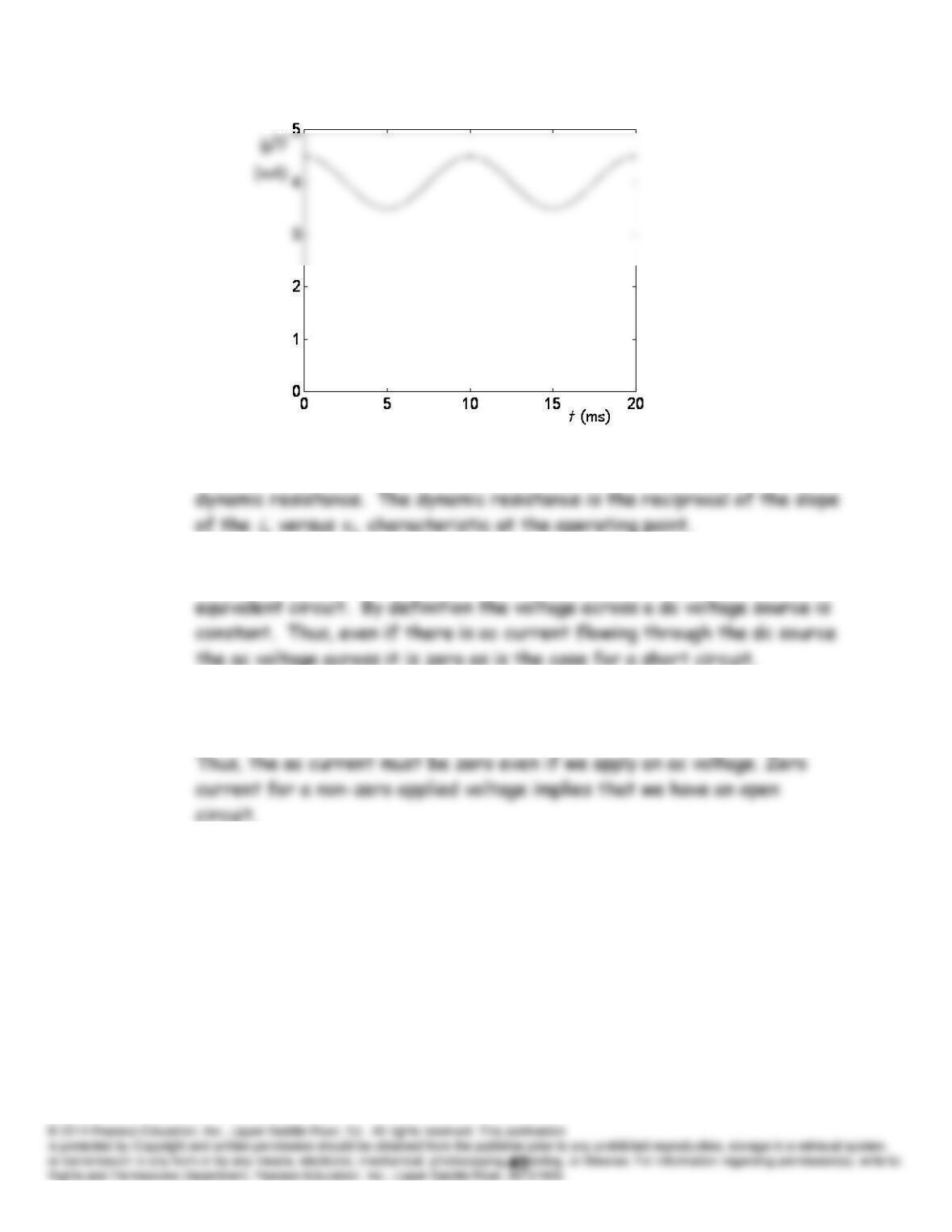
P10.77
IDQ
represents the dc component of the diode current with no signal
applied to the circuit, and
id
(
t
) represents the changes from the
Q
-point
P10.78 The small signal equivalent circuit of a diode is a resistance known as the
DD
P10.79 Dc sources voltage sources are replaced by short circuits in a small-signal
P10.80 We should replace dc current sources by open circuits in a small-signal
equivalent circuit. The current through a dc current source is constant.
P10.81* A plot of the device characteristic is:
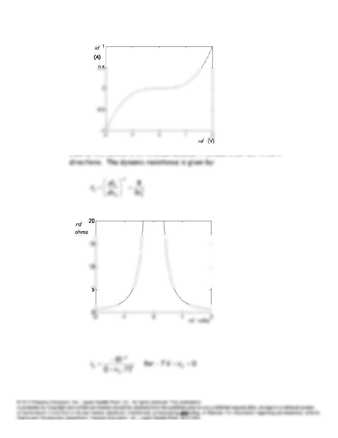
Clearly this device is not a diode because it conducts current in both
A plot of the dynamic resistance versus
vD
is:
P10.82 We are given
A plot of this is:
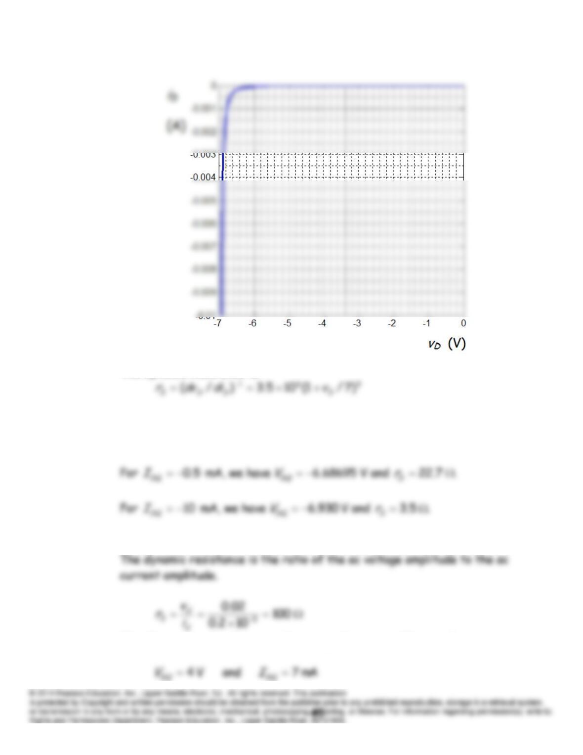
The dynamic resistance is:
To find the dynamic resistance at a given
Q
-point, we evaluate this
expression for
D DQ
vV
.
P10.83 We are given
vD
(
t
) = 4 + 0 .02cos(
t
) V and
iD
(
t
) = 7 + 0.2cos(
t
) mA.
The
Q
-point results if we set the ac signals to zero. Thus, we have
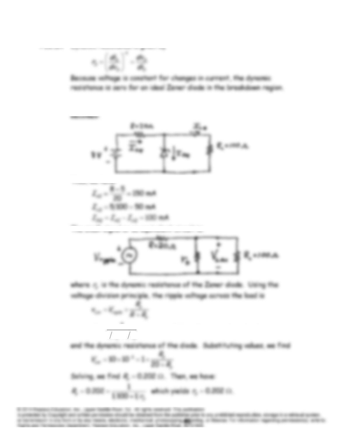
P10.84 Dynamic resistance is given by
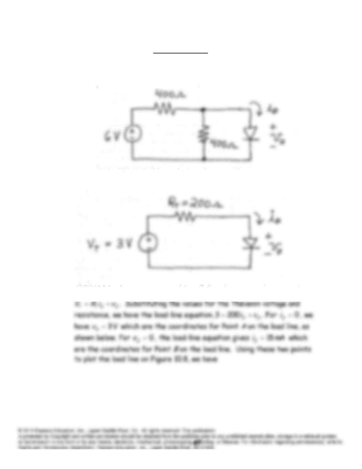
P10.85* To find the
Q
-point, we ignore the ac ripple voltage and the circuit
where
1
11
p
RRr
is the parallel combination of the load resistance
Practice Test
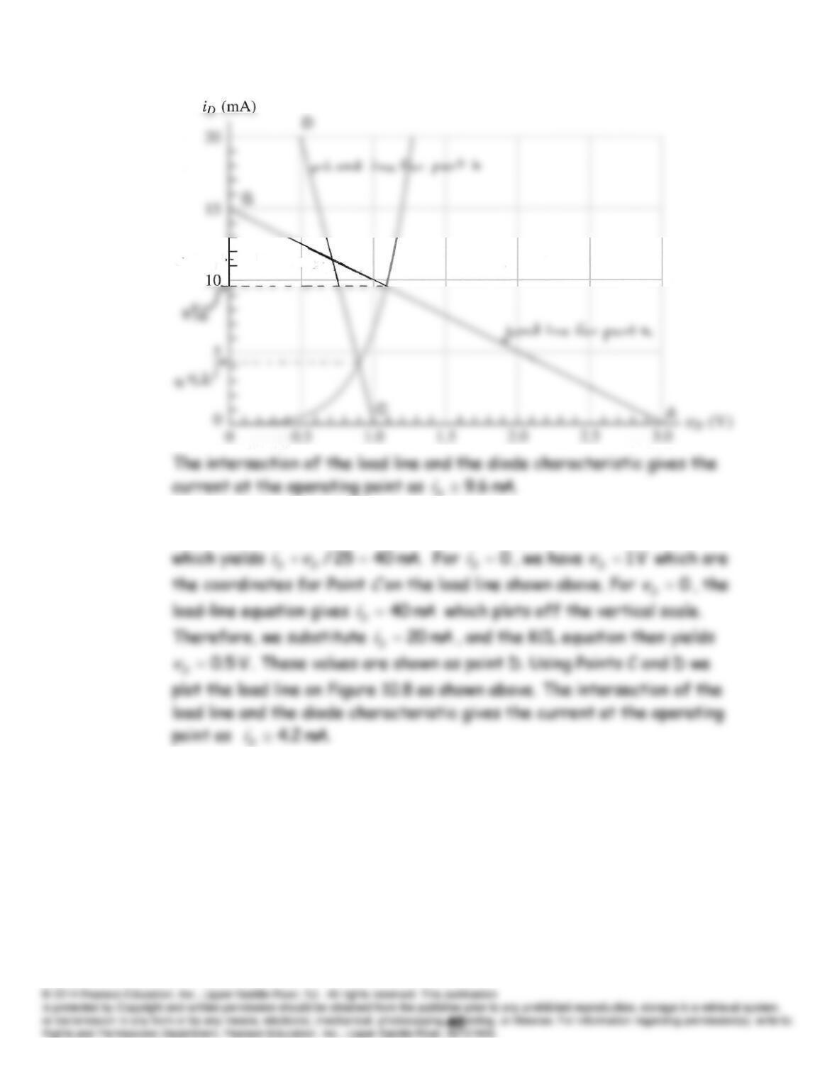
T10.1 (a) First, we redraw the circuit, grouping the linear elements to the left
of the diode.
Then, we determine the Thévenin equivalent for the circuit looking back
from the diode terminals.
Next, we write the KVL equation for the network, which yields
D
(b) First, we write the KCL equation at the top node of the network,
D
T10.2 If we assume that the diode is off (i.e., an open circuit), the circuit
becomes
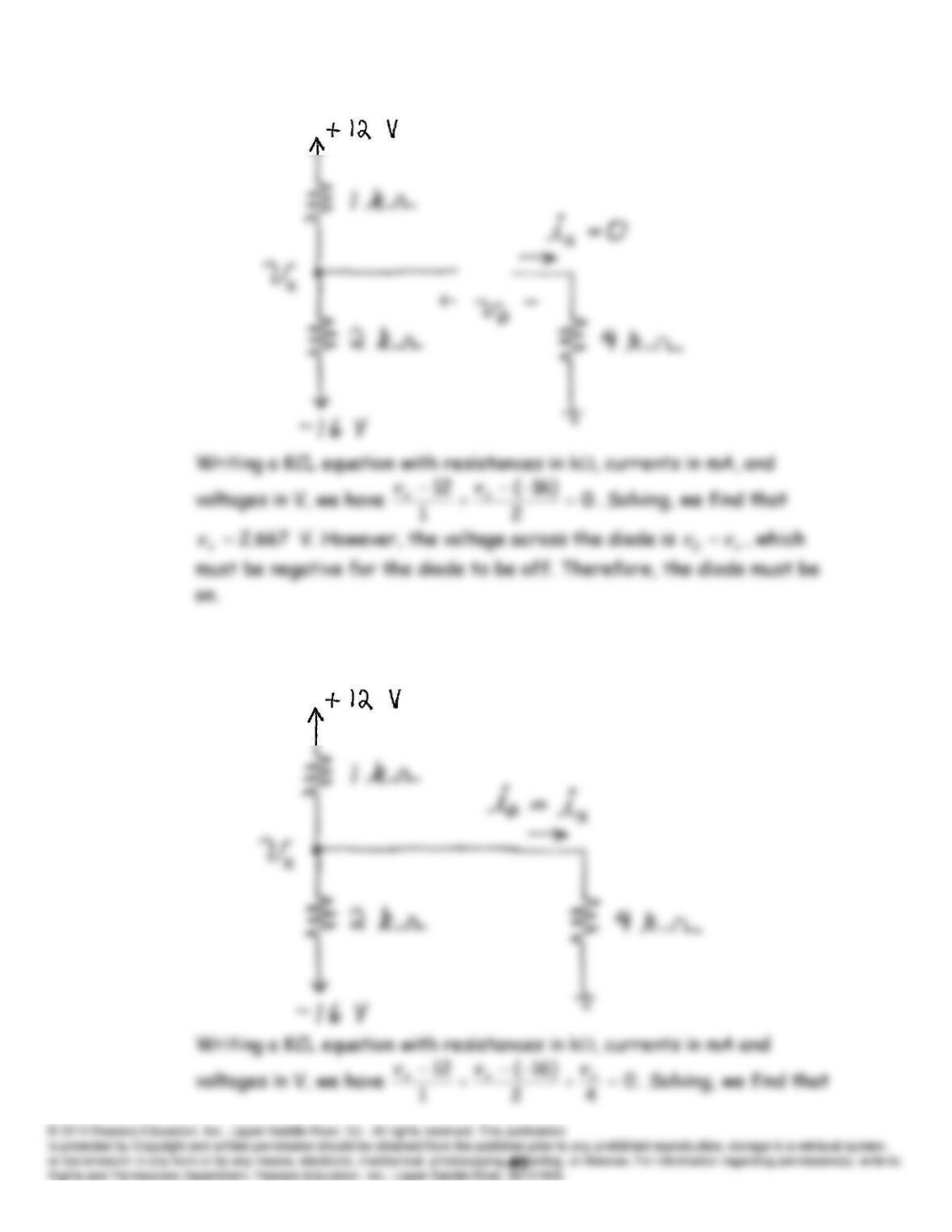
With the diode assumed to be on (i.e. a short circuit) the circuit
becomes
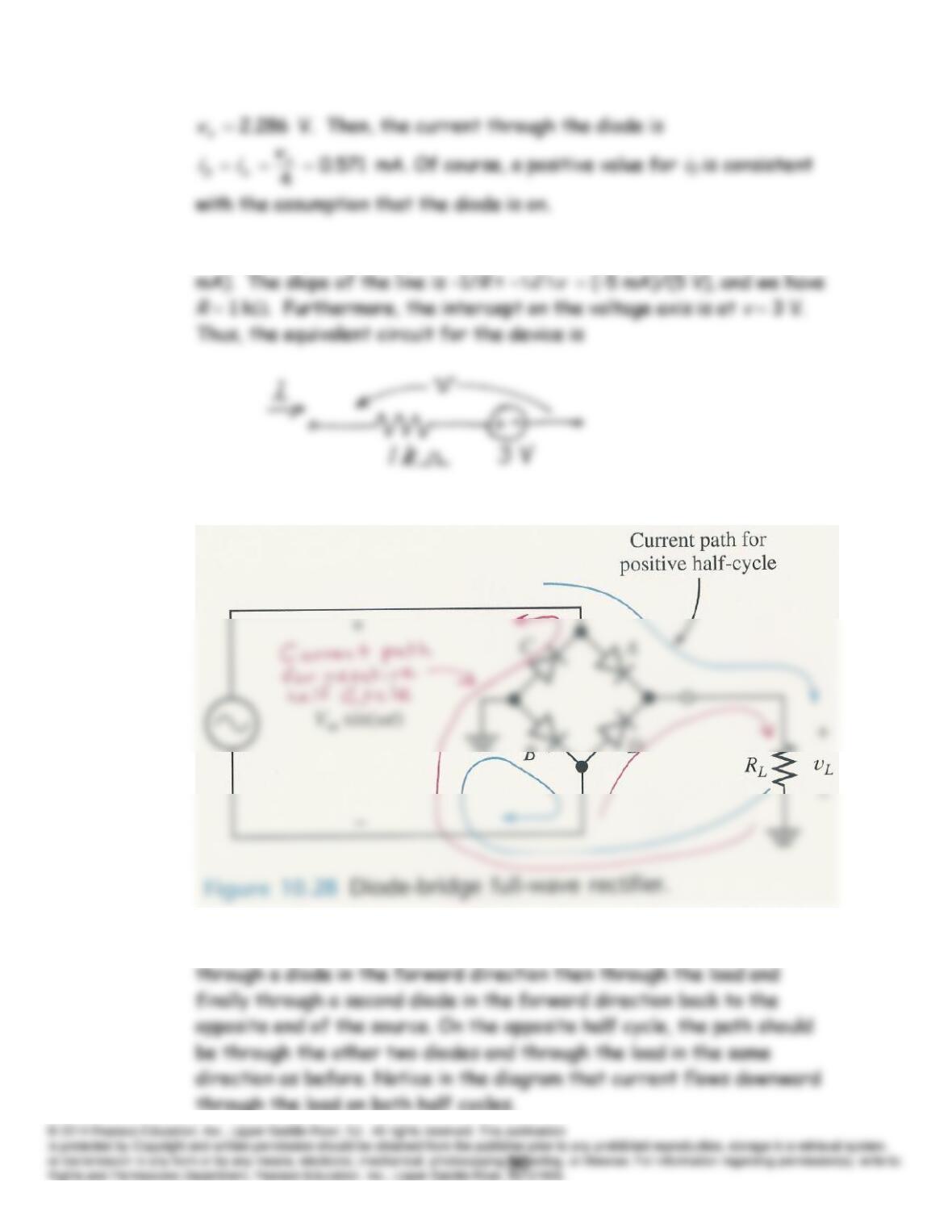
T10.3 We know that the line passes through the points (5 V, 2 mA) and (10 V, 7
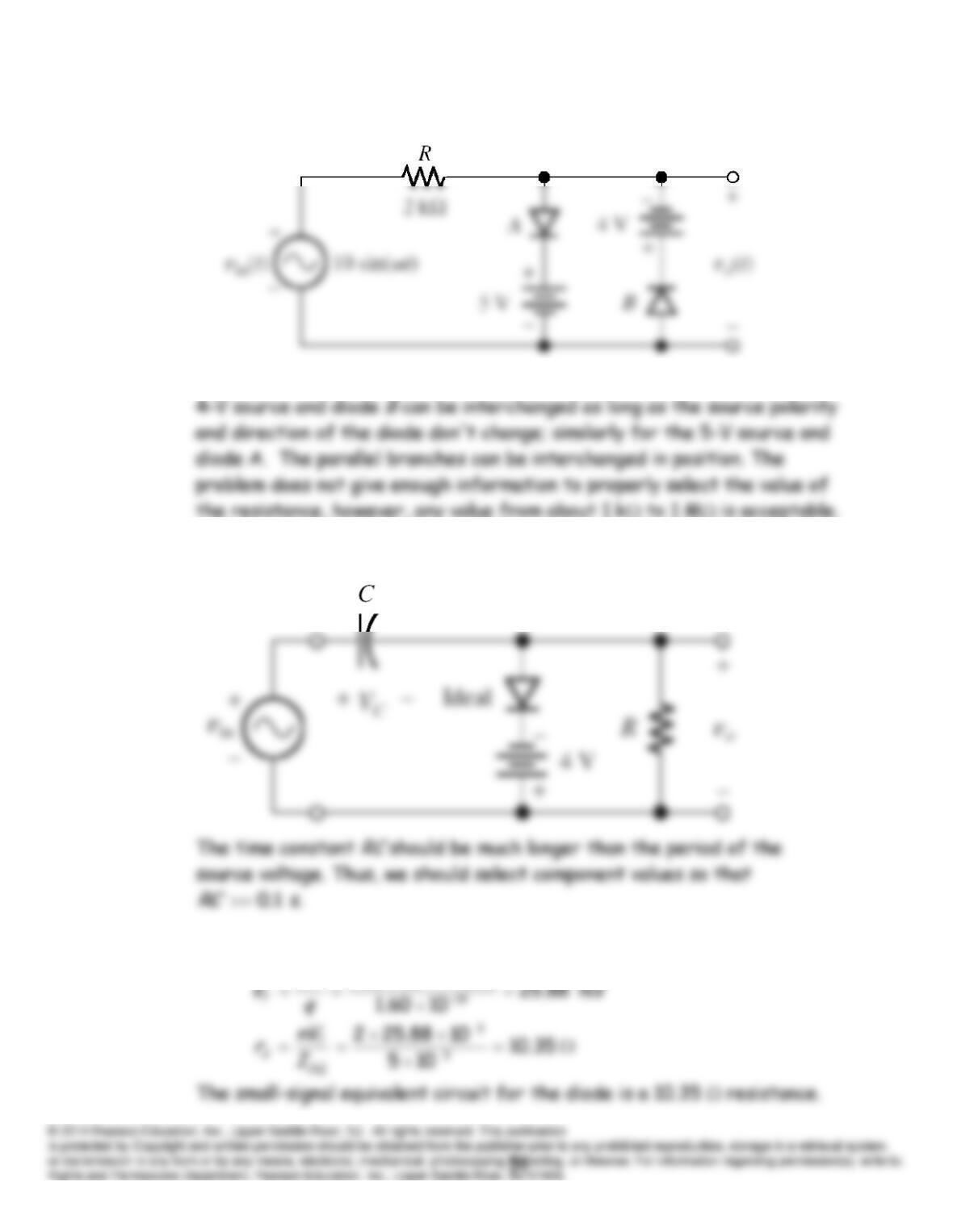
T10.4 The circuit diagram is:
Your diagram may be correct even if it is laid out differently. Check to
see that you have four diodes and that current flows from the source
T10.5 An acceptable circuit diagram is:
Your diagram may be somewhat different in appearance. For example, the
T10.6 An acceptable circuit diagram is:
T10.7 We have
3001038.1
23
kT