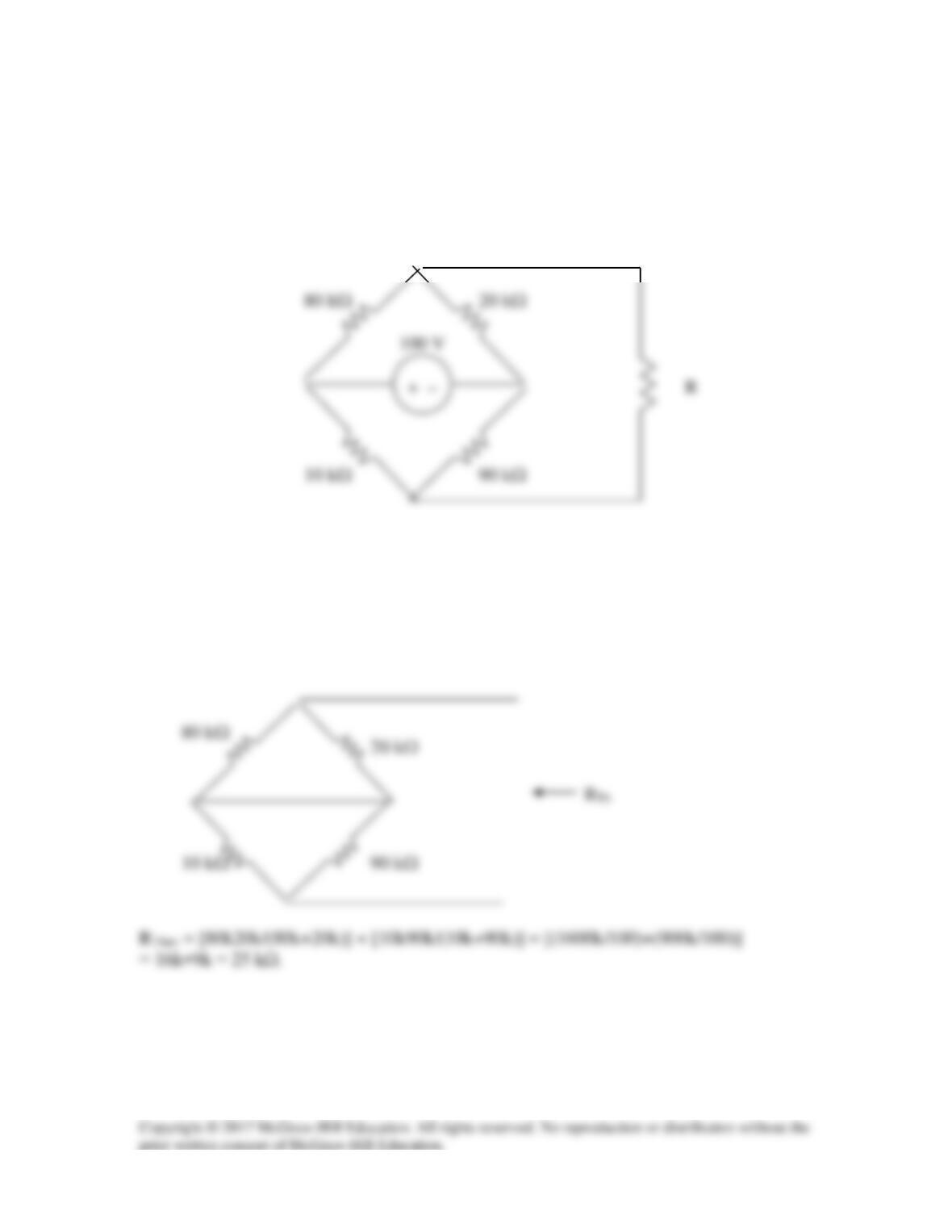
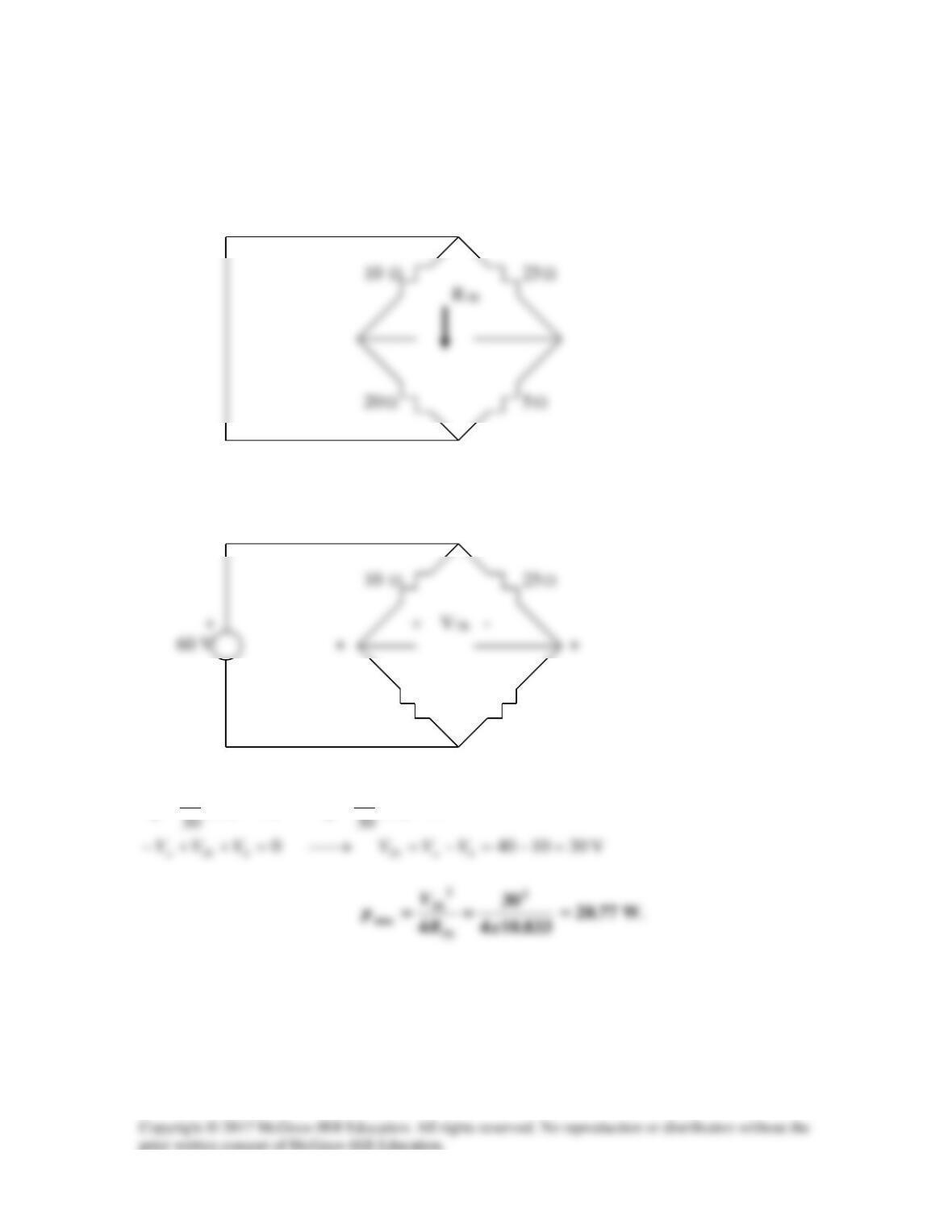
Solution 4.63
RN can be found using the circuit below.
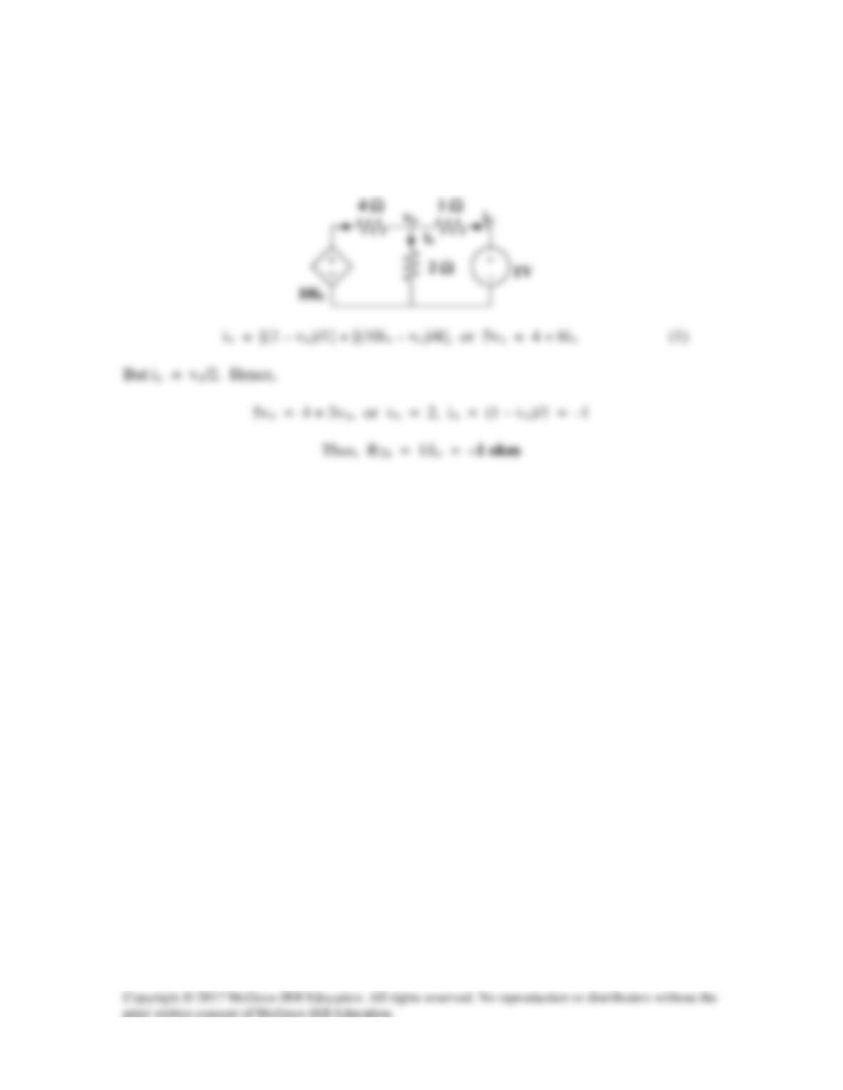
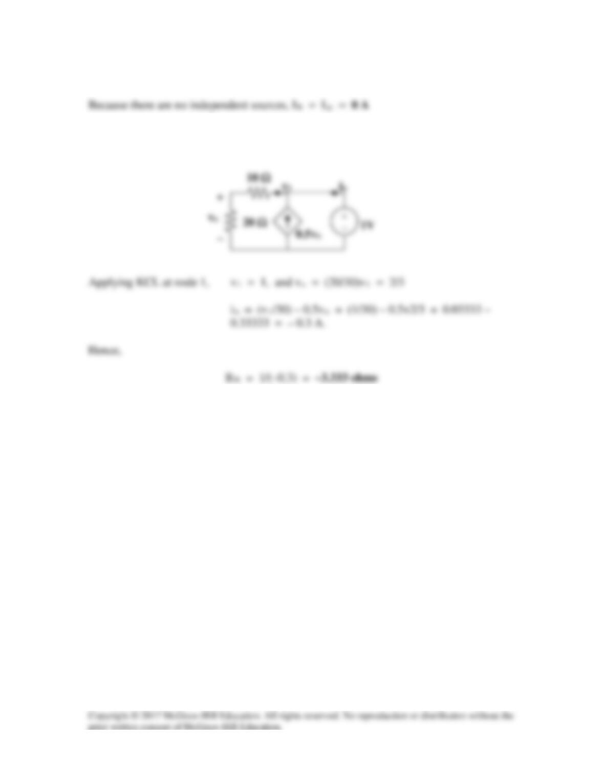
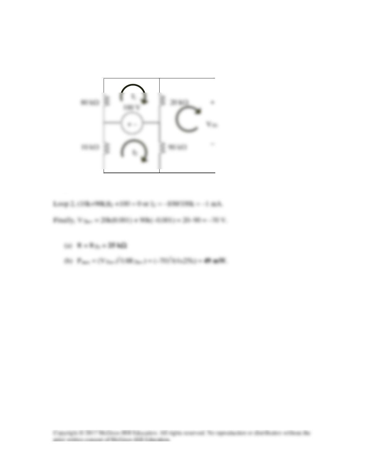
Solution 4.64
With no independent sources, VTh = 0 V. To obtain RTh, consider the circuit shown
below.
Solution 4.65
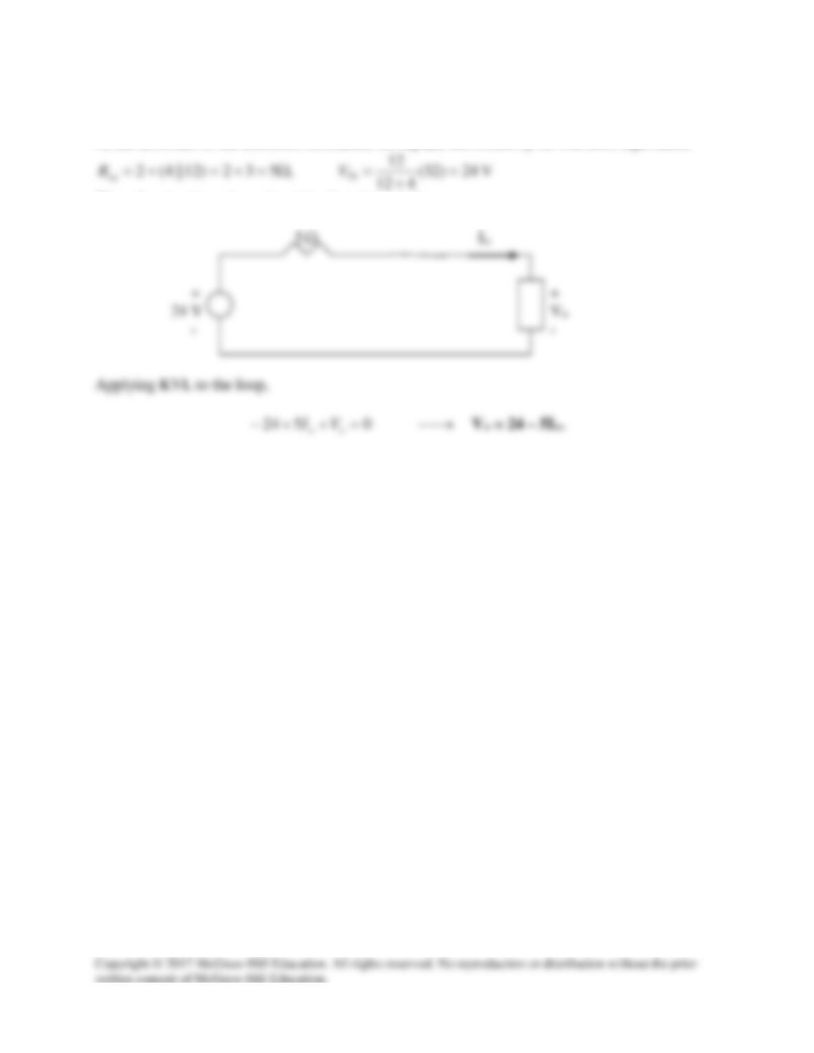
At the terminals of the unknown resistance, we replace the circuit by its Thevenin equivalent.
Thus, the circuit can be replaced by that shown below.
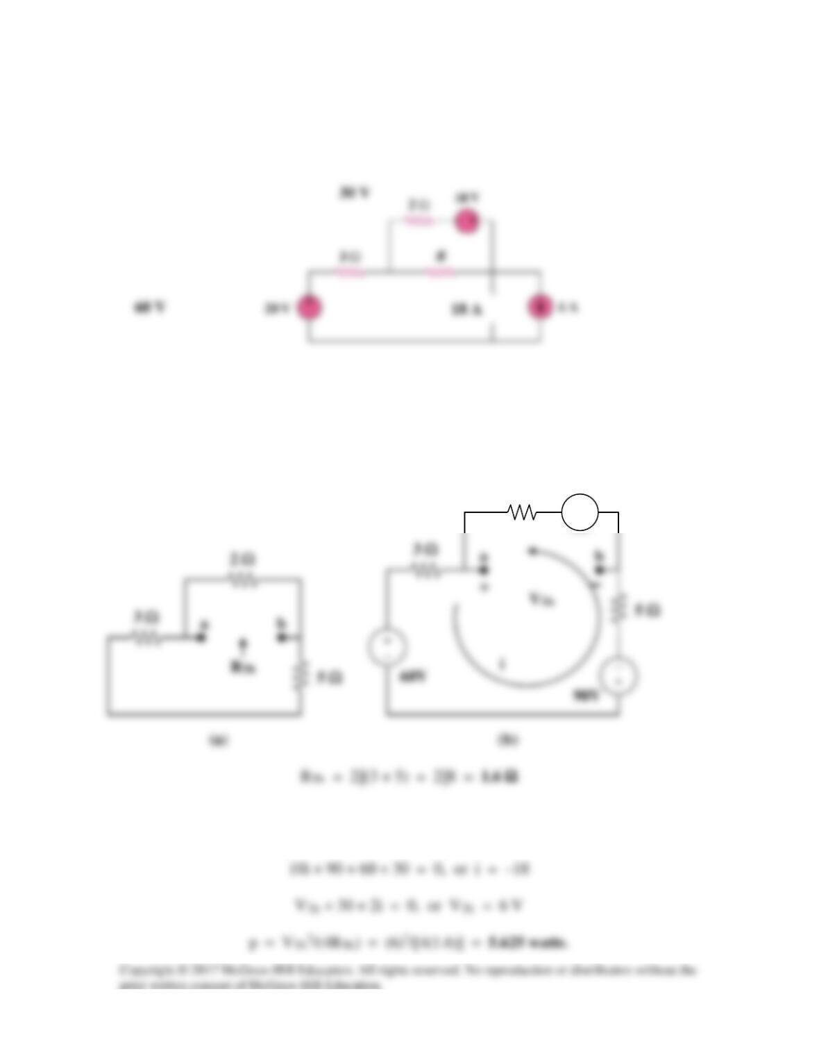
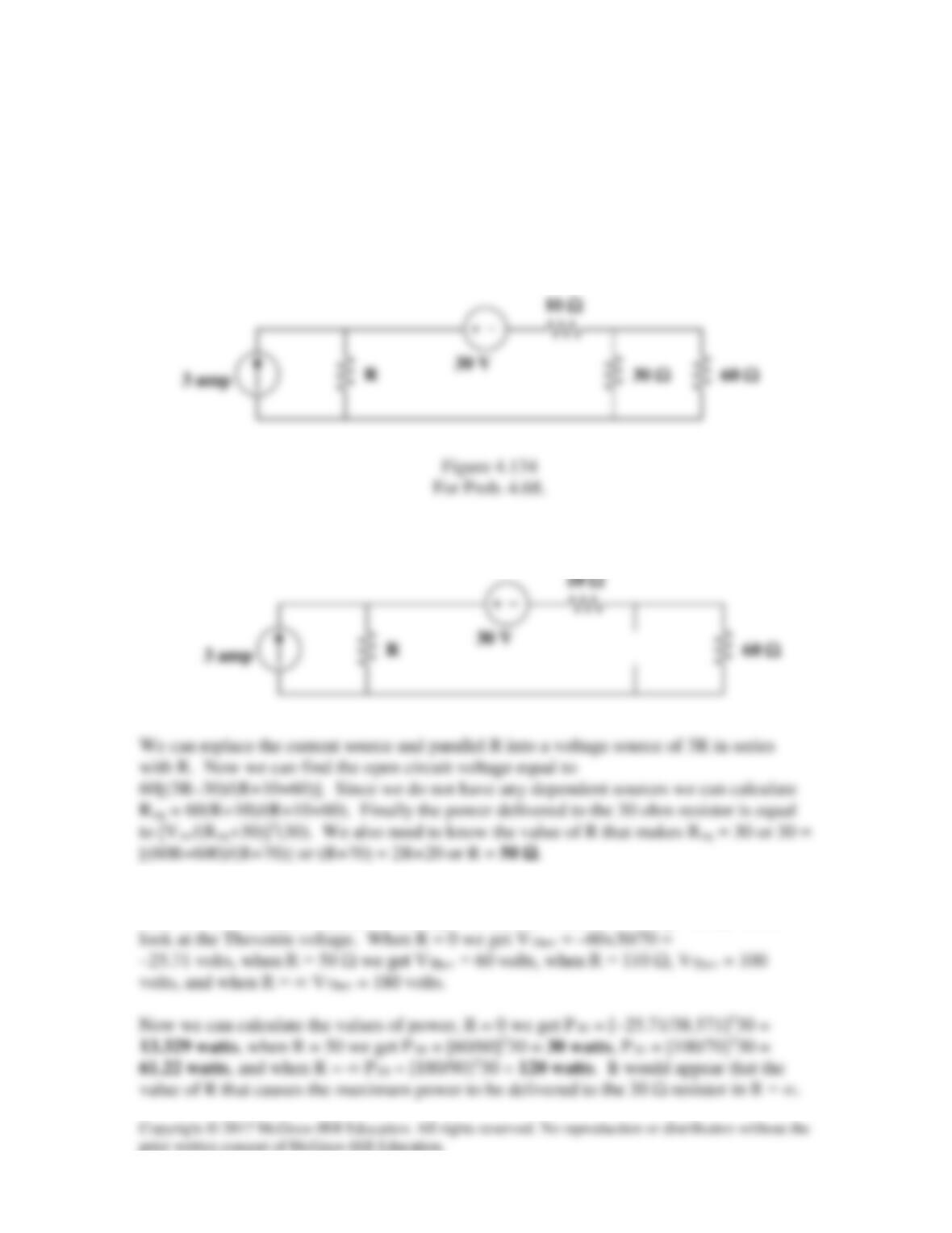
Solution 4.66
Find the maximum power that can be delivered to the resistor R in the circuit in Fig.
4.132.
Figure 4.132
For Prob. 4.66.
Solution
We first find the Thevenin equivalent at terminals a and b. We find RTh using the circuit
in Fig. (a).
3 Ω
2 Ω
3 Ω
By performing a source transformation on the given circuit, we obtain the circuit in (b).
We now use this to find VTh.
2 Ω
− +
30V
Solution 4.67
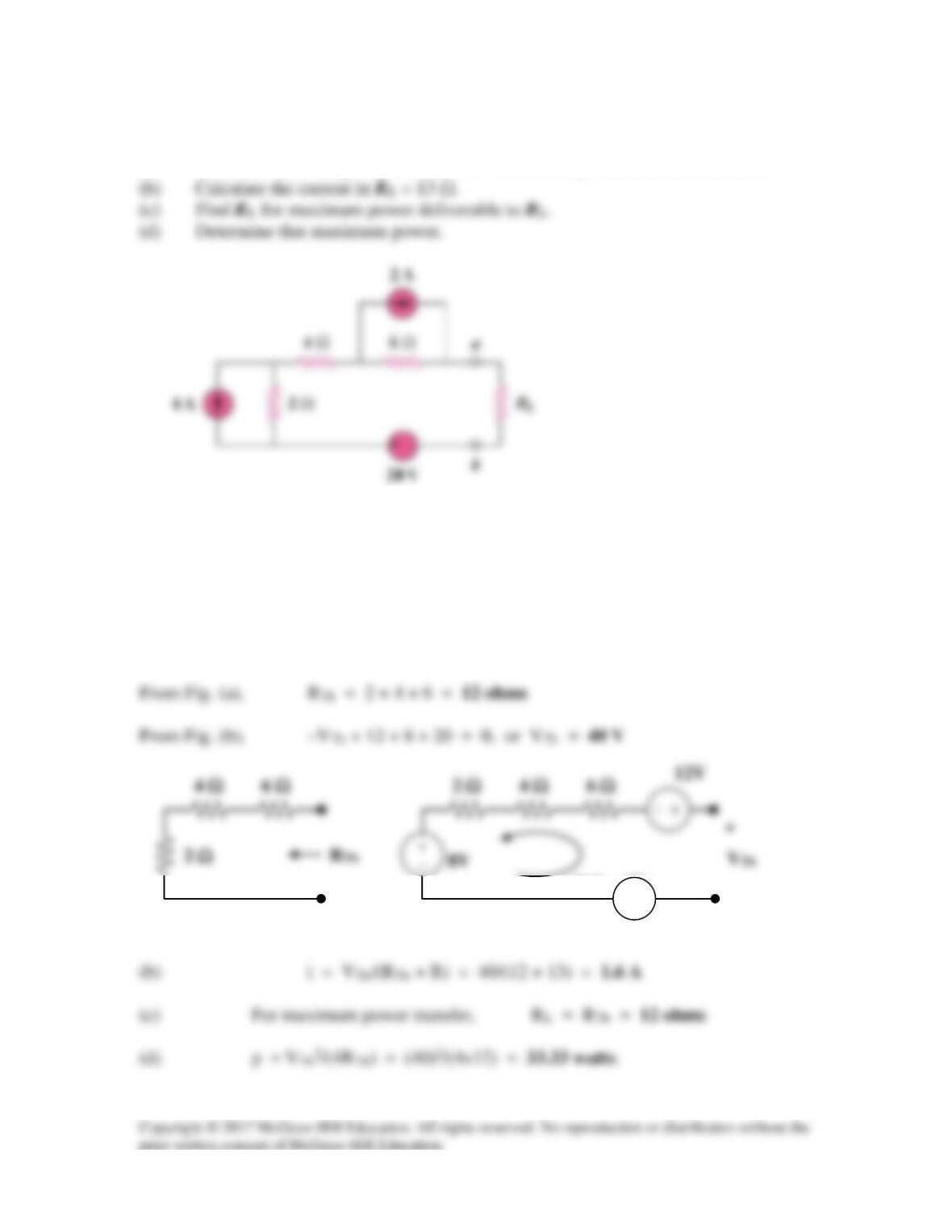
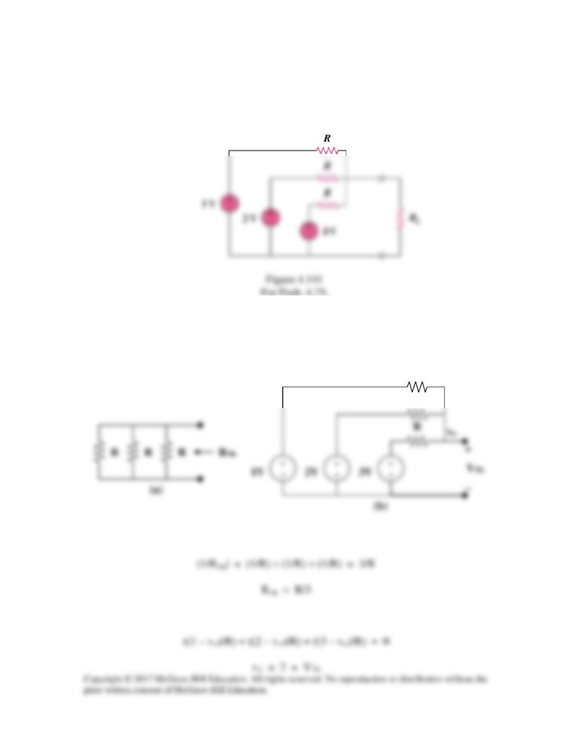
The variable resistor R in Fig. 4.133 is adjusted until it absorbs the maximum power from
the circuit. (a) Calculate the value of R for maximum power. (b) Determine the
maximum power absorbed by R.
Figure 4.133
For Prob. 4.67.
Solution
We first find the Thevenin equivalent. We find RTh using the circuit below.
We find VTh using the circuit below. We apply mesh analysis.
Loop 1, –100 + (80k+20k)I1 = 0 or I1 = 100/100k = 1 mA.
Solution 4.68
Consider the 30 Ω resistor. First compute the Thevenin equivalent circuit as seen by the
30 Ω resistor. Compute the value of R that results in Thevenin equivalent resistance
equal to the 30 Ω resistance and then calculate power delivered to the 30 Ω resistor. Now
let R = 0 Ω, 110 Ω, and ∞, calculate the power delivered to the 30 Ω resistor in each case.
What can you say about the value of R that will result in the maximum power that can be
delivered to the 30 Ω resistor?
Step 1. The first thing we need to do is to solve for VThev and Req as seen by the
30 ohm resistor.
Step 2. Let us look at the Thevenin equivalent resistance first. When R = 0, Req =
600/70 = 8.571 ohms, when R = 110, Req = 40 Ω, and when R = ∞, Req = 60 Ω. Now
v1
22 kΩ
v2
Figure 4.135
For Prob. 4.69.
Solution
First we need the Thevenin equivalent seen by the resistor R. To find the Thevenin
equivalent circuit we only need to find Voc and Isc.
Now we have [(v1–v2)/22k] – 0.006v2 + [(v1–0)/30k] = 0 and
To determine Isc we set v1 = 0 and find the current through the short. We have
Now we can find Isc = [(v2–0)/22k] + 0.006(58.667) = [(58.667)/22k] + 0.006(58.667) =
0.006vo
We can check the voltages by using PSpice and we get,
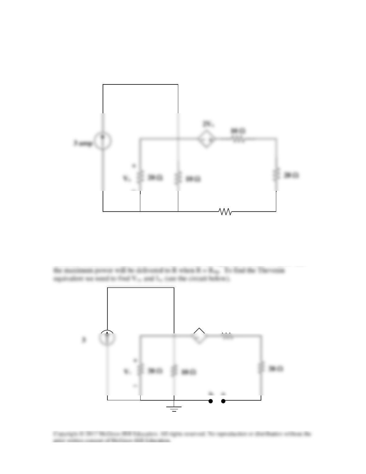
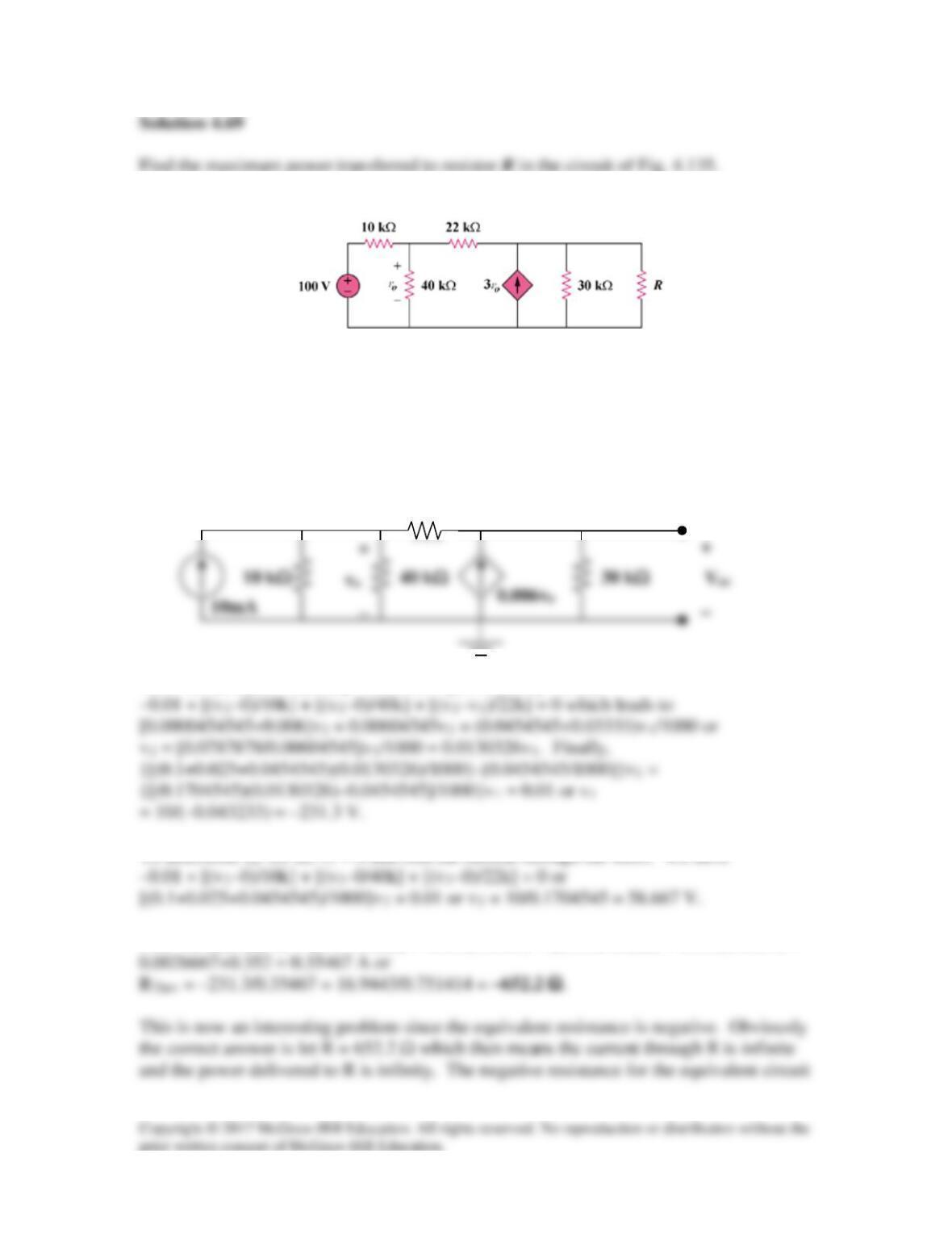
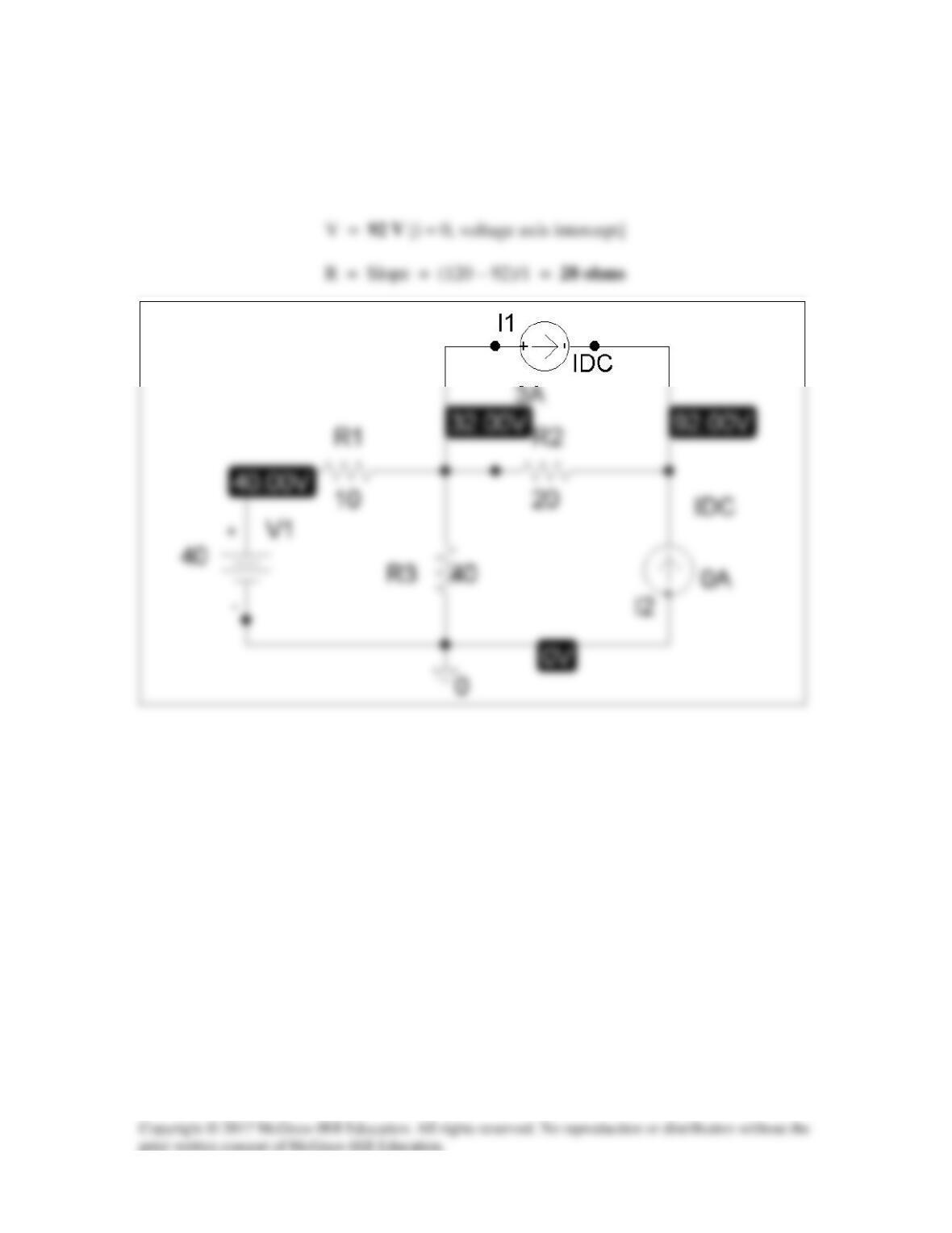
Solution 4.70
Determine the maximum power delivered to the variable resistor R shown in the circuit of
Fig. 4.136.
Figure 4.136
For Prob. 4.70.
Step 1. We need to start with finding the Thevenin equivalent circuit looking into the
terminals connected to the resistor R. Once we find the equivalent circuit we know that
R
−
2V
10 Ω
a
b

Let Voc = Vab and let Isc = Iab. We then need to analyze the separate circuits.
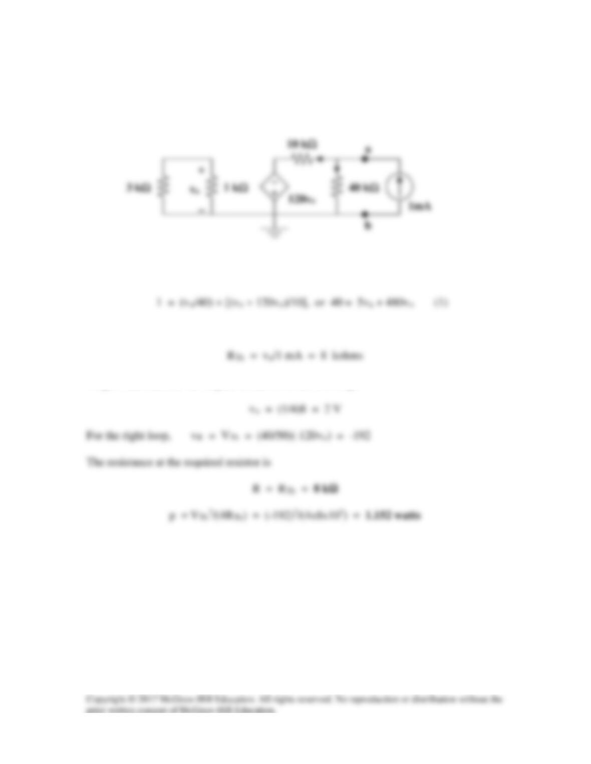
Solution 4.71
We need RTh and VTh at terminals a and b. To find RTh, we insert a 1–mA source at the
terminals a and b as shown below.
Assume that all resistances are in k ohms, all currents are in mA, and all voltages are in
volts. At node a,
The loop on the left side has no voltage source. Hence, vo = 0. From (1), va = 8 V.
To get VTh, consider the original circuit. For the left loop,
Solution 4.72
(a) For the circuit in Fig. 4.138, obtain the Thevenin equivalent at terminals a–b.
Figure 4.138
For Prob. 4.72.
Solution
(a) RTh and VTh are calculated using the circuits shown in Fig. (a) and (b)
respectively.
12V
(a)
20V
−
+ −
(b)
Solution 4.73
Find the Thevenin’s equivalent circuit across the terminals of R.
Ω==+= 833.1030/3255//2520//10
Th
R
Ω
Ω
–
Va Vb
20
Ω
5
Ω
– –
10)60(
5
,40)60(
20 ====
ba
VV
Solution 4.74
When RL is removed and Vs is short-circuited,
When RL is removed and we apply the voltage division principle,
Solution 4.75
For the circuit in Fig. 4.141, determine the value of R such that the maximum power
delivered to the load is 12 mW.
For Prob. 4.75.
Solution
We need to first find RTh and VTh.
R
Consider the circuit in Fig. (a).
From the circuit in Fig. (b),
R
R

For maximum power transfer,
RL = RTh = R/3
Solution 4.76
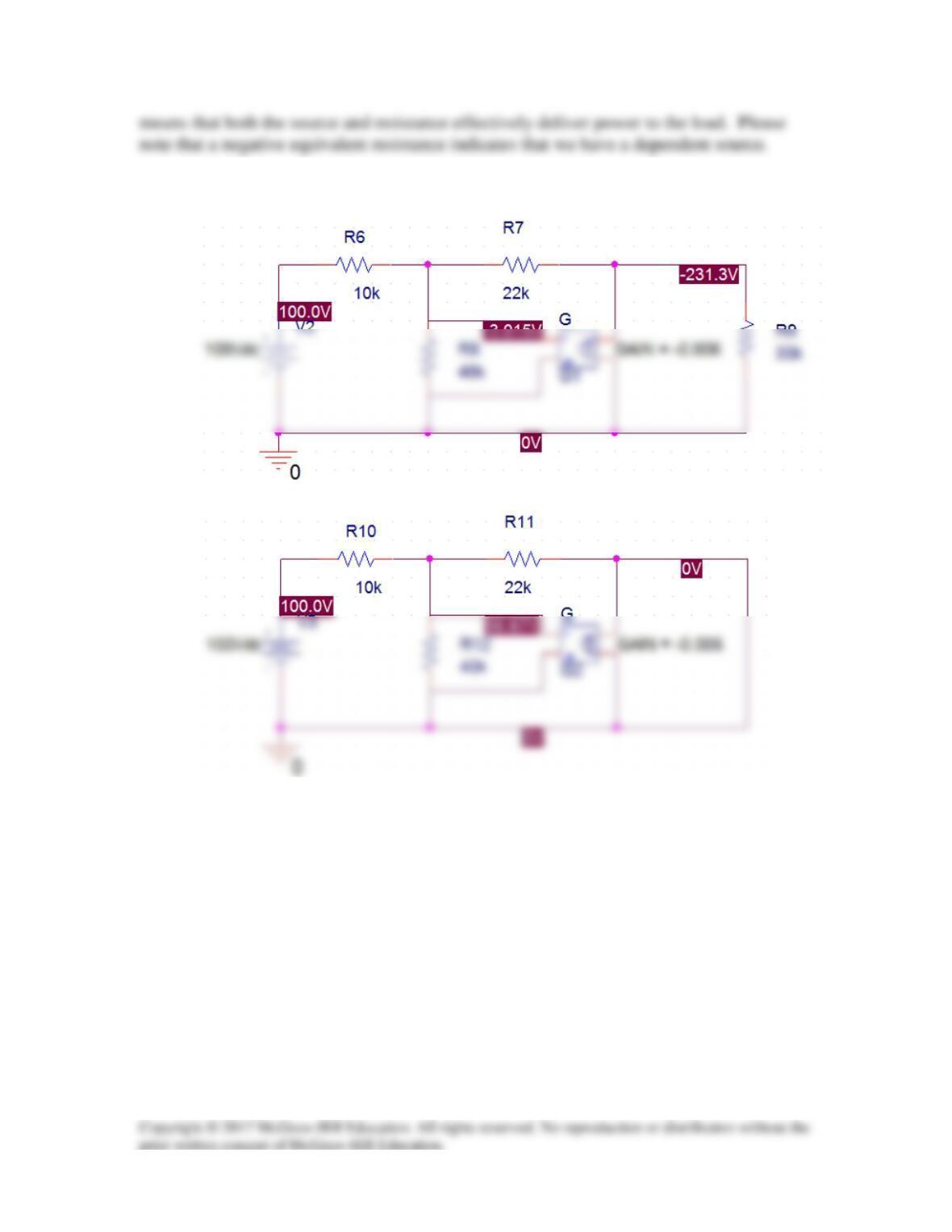
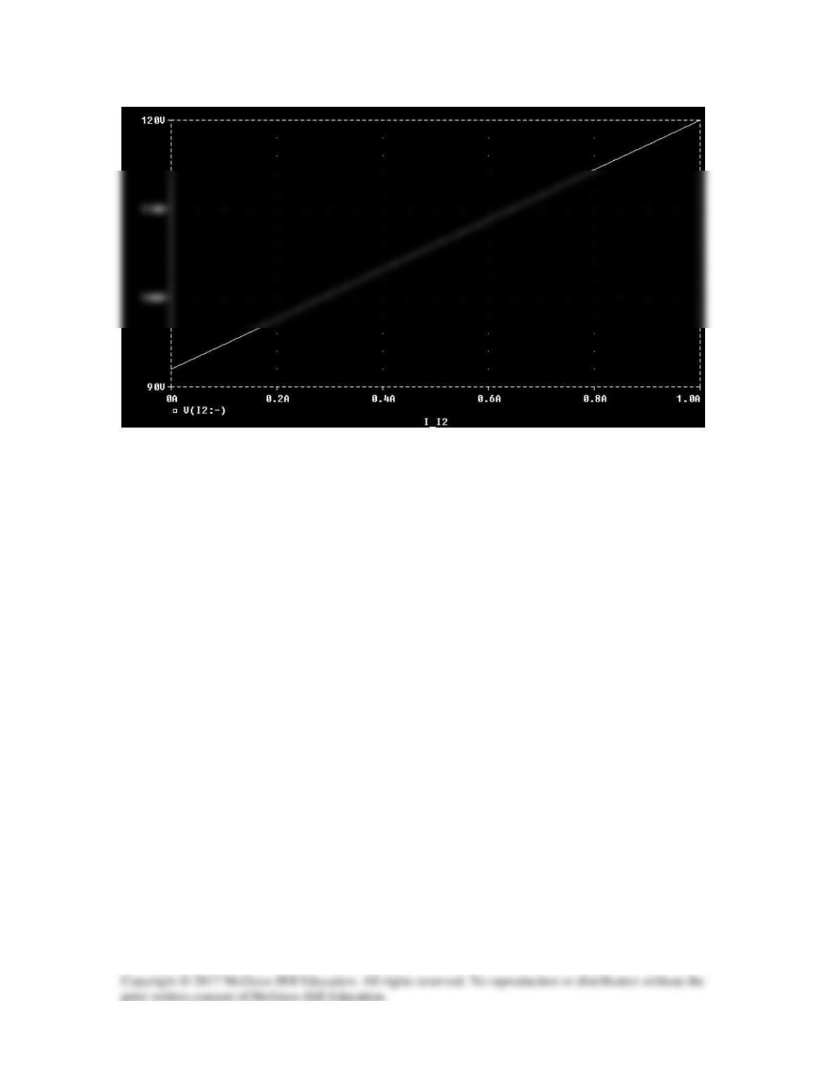
Follow the steps in Example 4.14. The schematic and the output plots are shown below.
From the plot, we obtain,
Solution 4.77
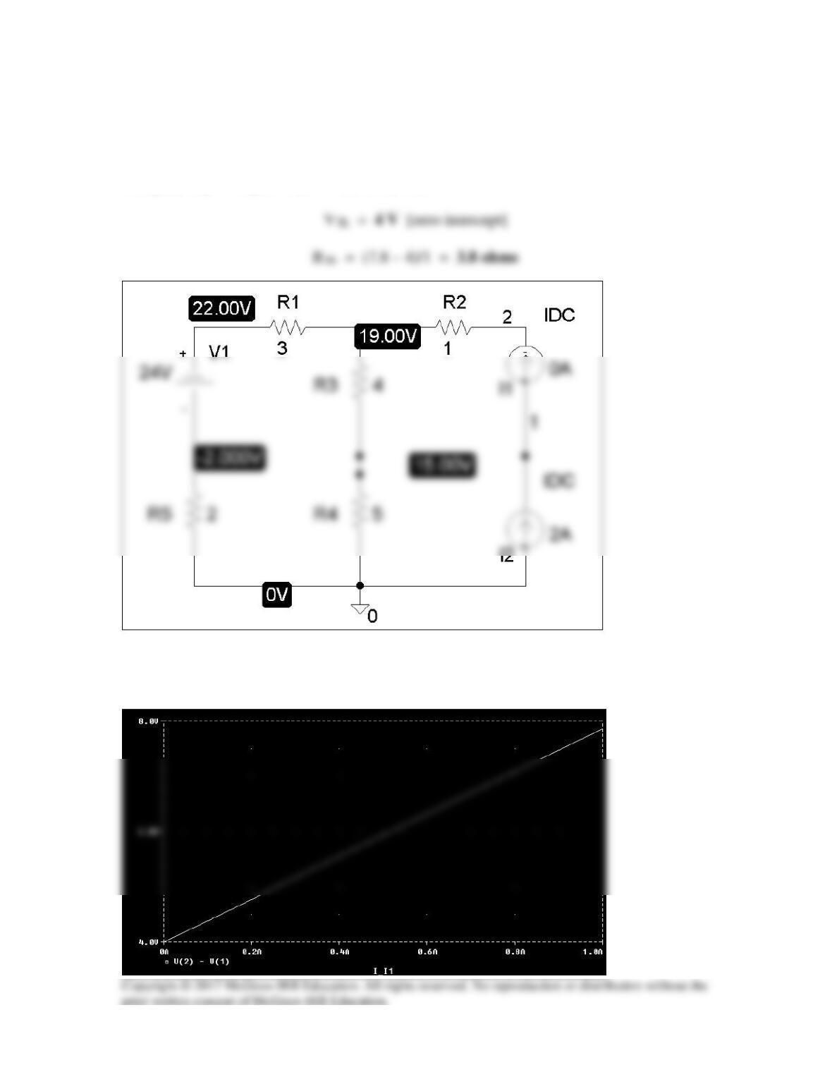
(a) The schematic is shown below. We perform a dc sweep on a current source, I1,
connected between terminals a and b. We label the top and bottom of source I1 as 2 and
1 respectively. We plot V(2) – V(1) as shown.
(b) Everything remains the same as in part (a) except that the current source, I1, is
connected between terminals b and c as shown below. We perform a dc sweep on
I1 and obtain the plot shown below. From the plot, we obtain,