Unit 10 Design Solutions
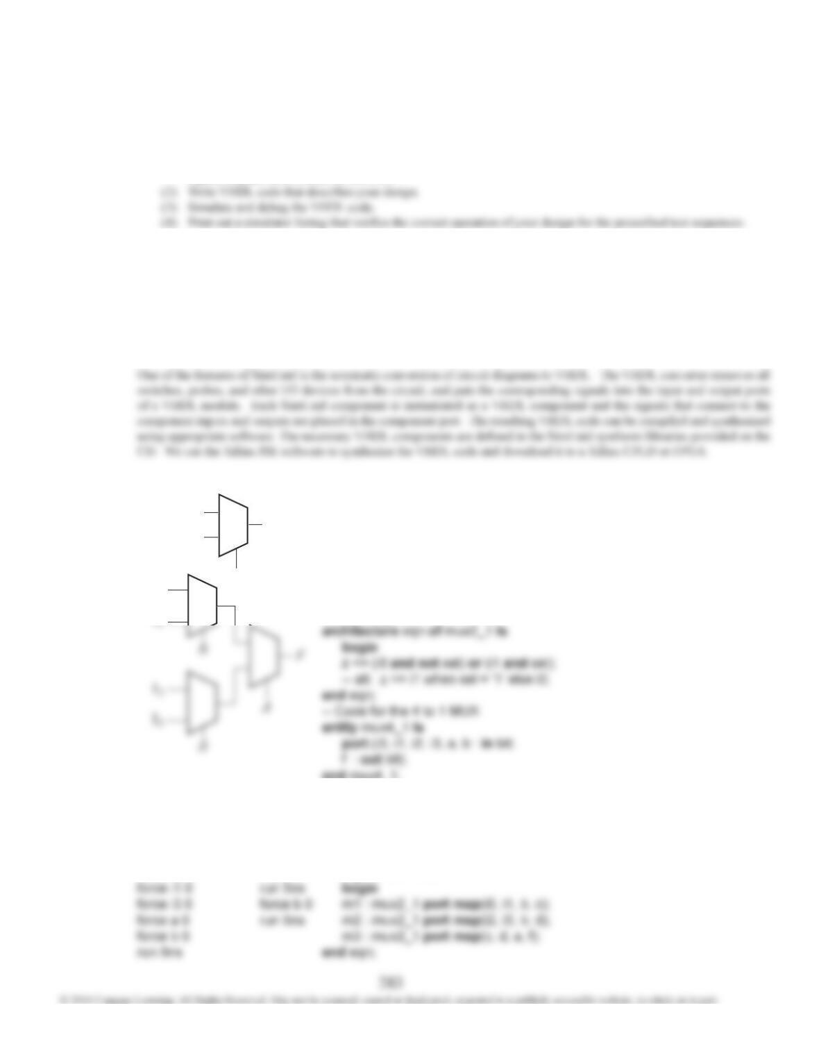
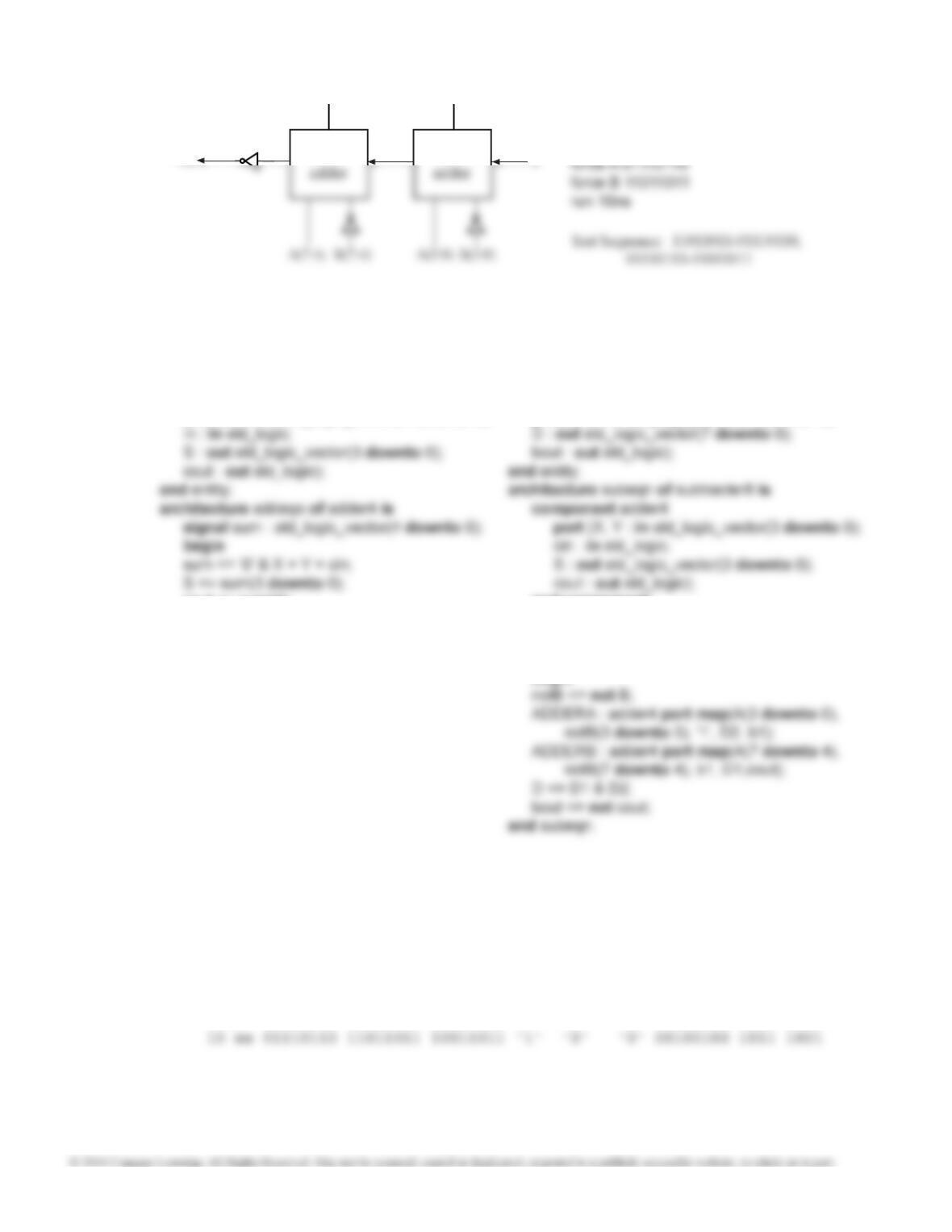
10.A
I0
I1
Z
SEL
I0
I1
— Code for the 2 to 1 MUX
entity mux2_1 is
port (i0, i1, sel : in bit;
z : out bit);
end mux2_1;
end mux4_1;
architecture eqn of mux4_1 is
component mux2_1 is
port (i0, i1, sel : in bit;
z : out bit);
end component;
signal c, d : bit;
Test Sequence: I0 = I2 = 1,
I1 = I3 = 0, AB = 00, 01, 11, 10.
Command Sequence:
force i0 1
force i2 1
Output (from DirectVHDL):
Time i0 i1 i2 i3 a b f d c
0 ns ‘1’ ‘0’ ‘1’ ‘0’ ‘0’ ‘0’ ‘1’ ‘1’ ‘1’
5 ns ‘1’ ‘0’ ‘1’ ‘0’ ‘0’ ‘1’ ‘0’ ‘0’ ‘0’
10 ns ‘1’ ‘0’ ‘1’ ‘0’ ‘1’ ‘1’ ‘0’ ‘0’ ‘0’
15 ns ‘1’ ‘0’ ‘1’ ‘0’ ‘1’ ‘0’ ‘1’ ‘1’ ‘1’
force b 1
run 5ns
force a 1
Solutions to Unit 10 Design and Simulation Problems
Assignment 1:
We use Problems 10.A through 10.M to introduce students to the use of a VHDL Simulator for testing and debugging their
VHDL code. We ask our students to do the following:
(1) Work out the logic design for your assigned problem, including a block diagram for the main module showing
inputs, outputs, and internal connections.
Test sequences for problems 10.A through 10.N are given in FLD. The command sequences and the listing outputs given in
the solutions that follow make use of the DirectVHDL simulator, which is provided on the CD.
Assignment 2:
In Unit 8, we asked students to design and simulate a combinational circuit using NAND and NOR gates. In this assignment,
we ask the students to convert their SimUaid circuit from Unit 8 to VHDL code, compile the VHDL code, download it to a
Xilinx CPLD or FPGA board, and test its operation.
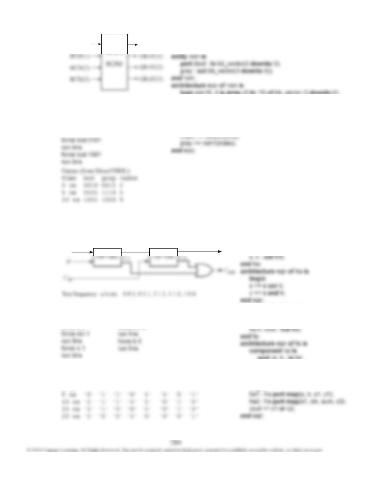
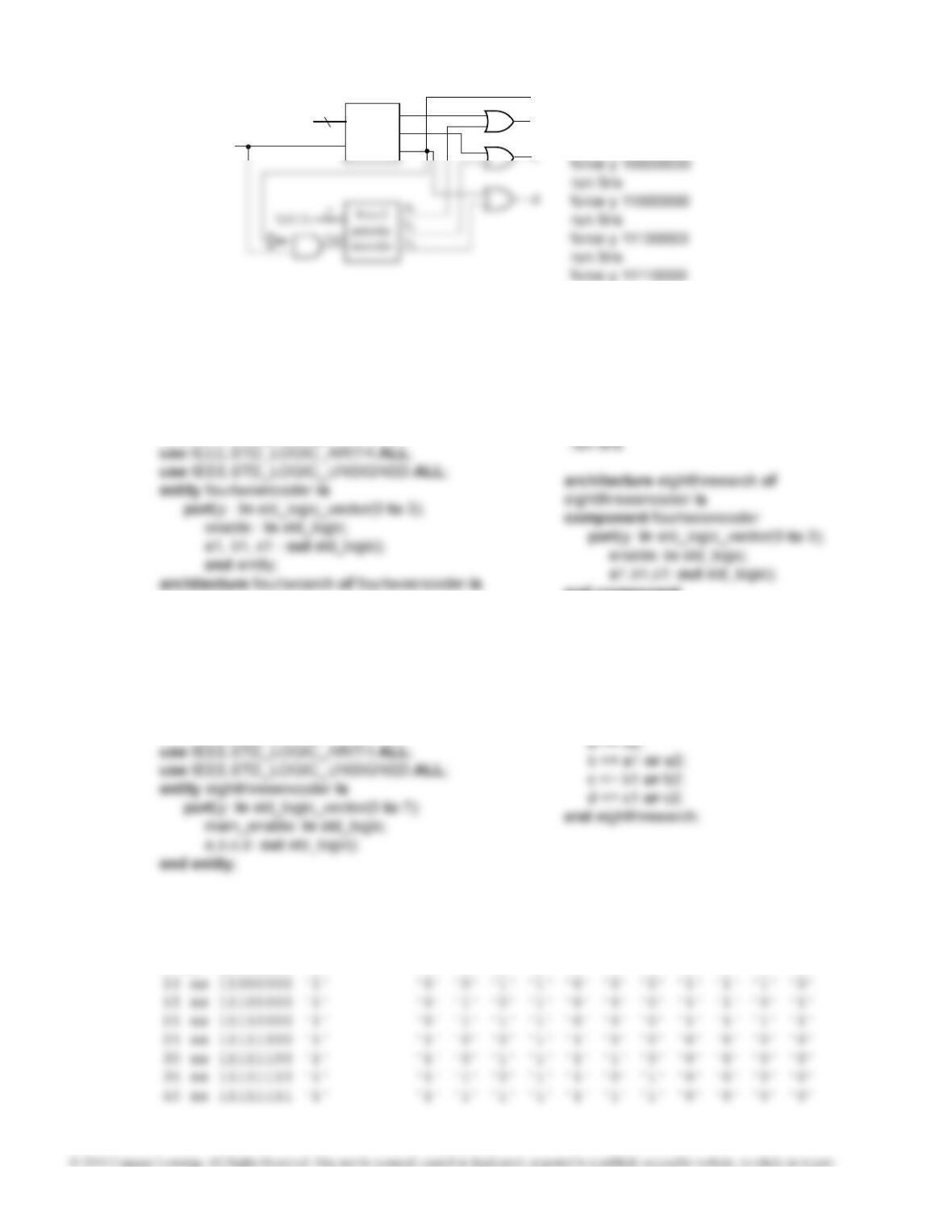
Unit 10 Design Solutions
10.C
A
S
1
— Code for the half adder
entity ha is
port (a, b : in bit;
— Code for the full adder
entity fa is
port (a, b, cin : in bit;
port (a, b : in bit;
s, c : out bit);
end component;
signal s1, c1, c2 : bit;
begin
Command Sequence:
force a 0
force b 0
Output (from DirectVHDL):
Time a b cin sum cout c2 c1 s1
0 ns ‘0’ ‘0’ ‘1’ ‘1’ ‘0’ ‘0’ ‘0’ ‘0’
force a 1
run 5ns
force cin 0
Note: See solution to Problem 4.40 for derivation of the half-adder
10.B
BCD(0) GRAY(0)
library bitlib;
use bitlib.bit_pack.all;
type rom16_4 is array (0 to 15) of bit_vector (3 downto 0);
constant rom1 : rom16_4 := (“0000”, “0001”, “0011”, “0010”,
“0110”, “1110”, “1010”, “1011”, “1001”, “1000”, others =>
“1111”);
signal index : integer range 0 to 15;
begin
Command Sequence:
force bcd 0010
run 5ns
Test Sequence: BCD = 0010, 0101, 1001.
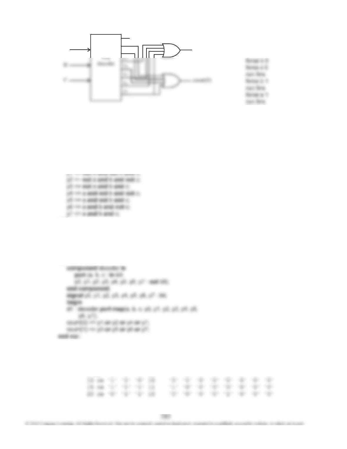
Unit 10 Design Solutions
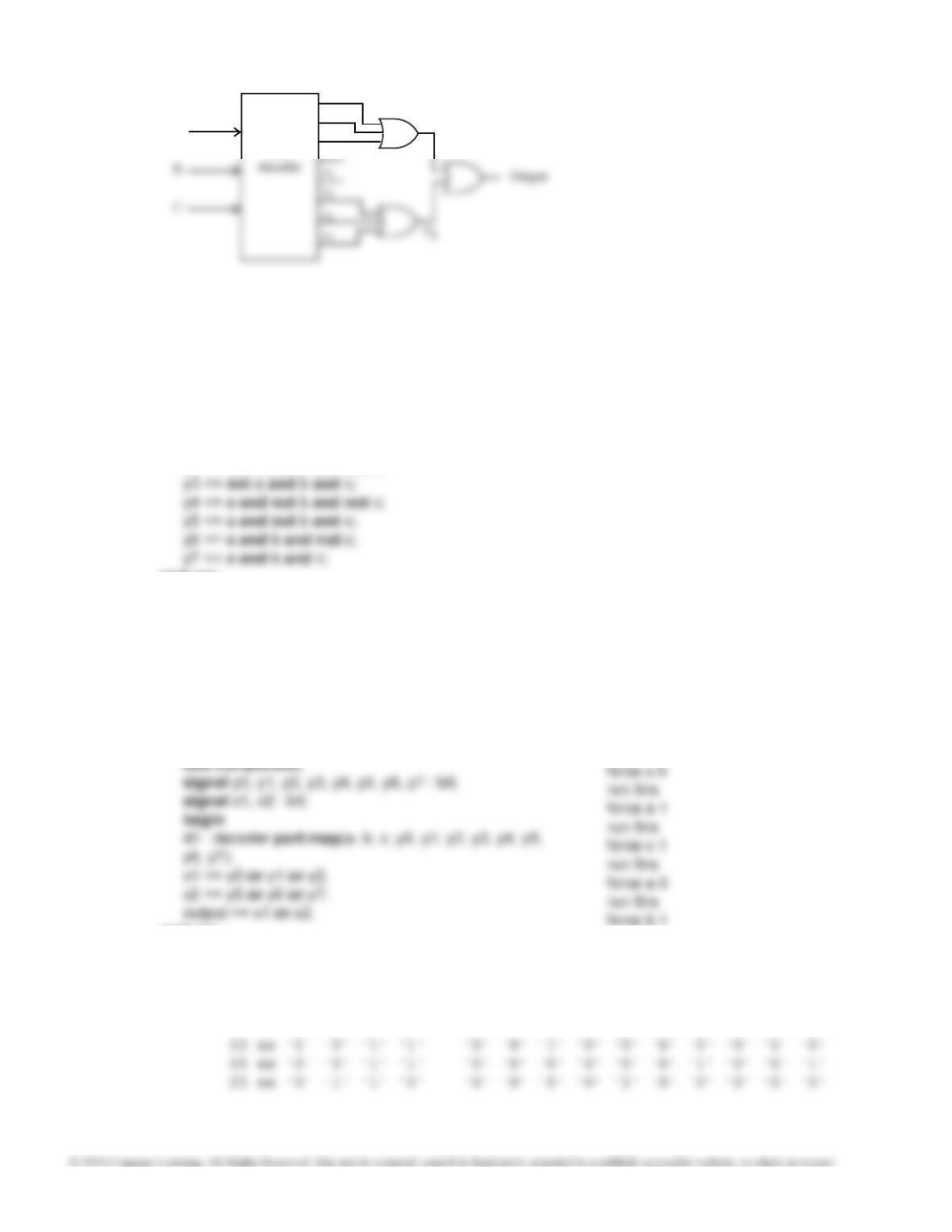
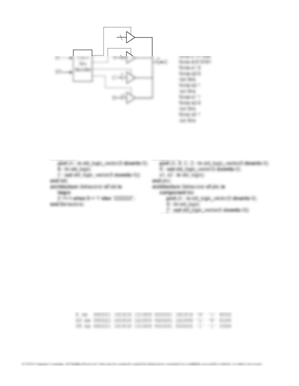
10.D y0
y1
y2
3 – to – 8
count(1)
A
Test Sequence: a b c = 0 0 0, 0 1 0, 1 1 0, 1 1 1, 0 1 1.
Command Sequence:
force a 0
force c 1
run 5ns
force a 0
run 5ns
Output (from DirectVHDL):
Time a b c count y7 y6 y5 y4 y3 y2 y1 y0
0 ns ‘0’ ‘0’ ‘0’ 00 ‘0’ ‘0’ ‘0’ ‘0’ ‘0’ ‘0’ ‘0’ ‘1’
5 ns ‘0’ ‘1’ ‘0’ 01 ‘0’ ‘0’ ‘0’ ‘0’ ‘0’ ‘1’ ‘0’ ‘0’
— Code for the 3 to 8 decoder
entity decoder is
port (a, b, c : in bit;
y0, y1, y2, y3, y4, y5, y6, y7 : out bit);
end decoder;
architecture eqn of decoder is
begin
y0 <= not a and not b and not c;
end eqn;
— Code for the main module
entity fa is
port (a, b, c : in bit;
count : out bit_vector(1 downto 0));
end fa;
architecture eqn of fa is
286
Unit 10 Design Solutions
10.E
BCD(0) Seven(0) = X1
16 x 7
Seven(1) = X2
library bitlib;
use bitlib.bit_pack.all;
entity rom is
=> “0000000”);
signal index : integer range 0 to 15;
begin
index <= vec2int(bcd);
seven <= rom1(index);
end eqn;
Test Sequence: BCD = 0000, 0001, 1000, 1001.
Command Sequence:
force bcd 0000
run 5ns
Output (from DirectVHDL):
Time bcd seven index
0 ns 0000 3f 0
287
Unit 10 Design Solutions
10.F y0
y1
y2
y3
3 – to – 8
line
A
X
1
entity decoder is
port (a, b, c : in bit;
y0, y1, y2, y3, y4, y5, y6, y7 : out bit);
end decoder;
architecture eqn of decoder is
begin
y0 <= not a and not b and not c;
y1 <= not a and not b and c;
y2 <= not a and b and not c;
end eqn;
— Code for the main module
entity main is
port (a, b, c : in bit;
output : out bit);
end main;
architecture eqn of main is
component decoder is
port (a, b, c : in bit;
y0, y1, y2, y3, y4, y5, y6, y7 : out bit);
end eqn;
Test Sequence:
a b c = 0 0 0, 1 0 0, 1 0 1, 0 0 1, 0 1 1.
Command Sequence:
force a 0
force b 0
run 5ns
Output (from DirectVHDL):
Time a b c output y7 y6 y5 y4 y3 y2 y1 y0 x2 x1
0 ns ‘0’ ‘0’ ‘0’ ‘1’ ‘0’ ‘0’ ‘0’ ‘0’ ‘0’ ‘0’ ‘0’ ‘1’ ‘0’ ‘1’
5 ns ‘1’ ‘0’ ‘0’ ‘0’ ‘0’ ‘0’ ‘0’ ‘1’ ‘0’ ‘0’ ‘0’ ‘0’ ‘0’ ‘0’
288
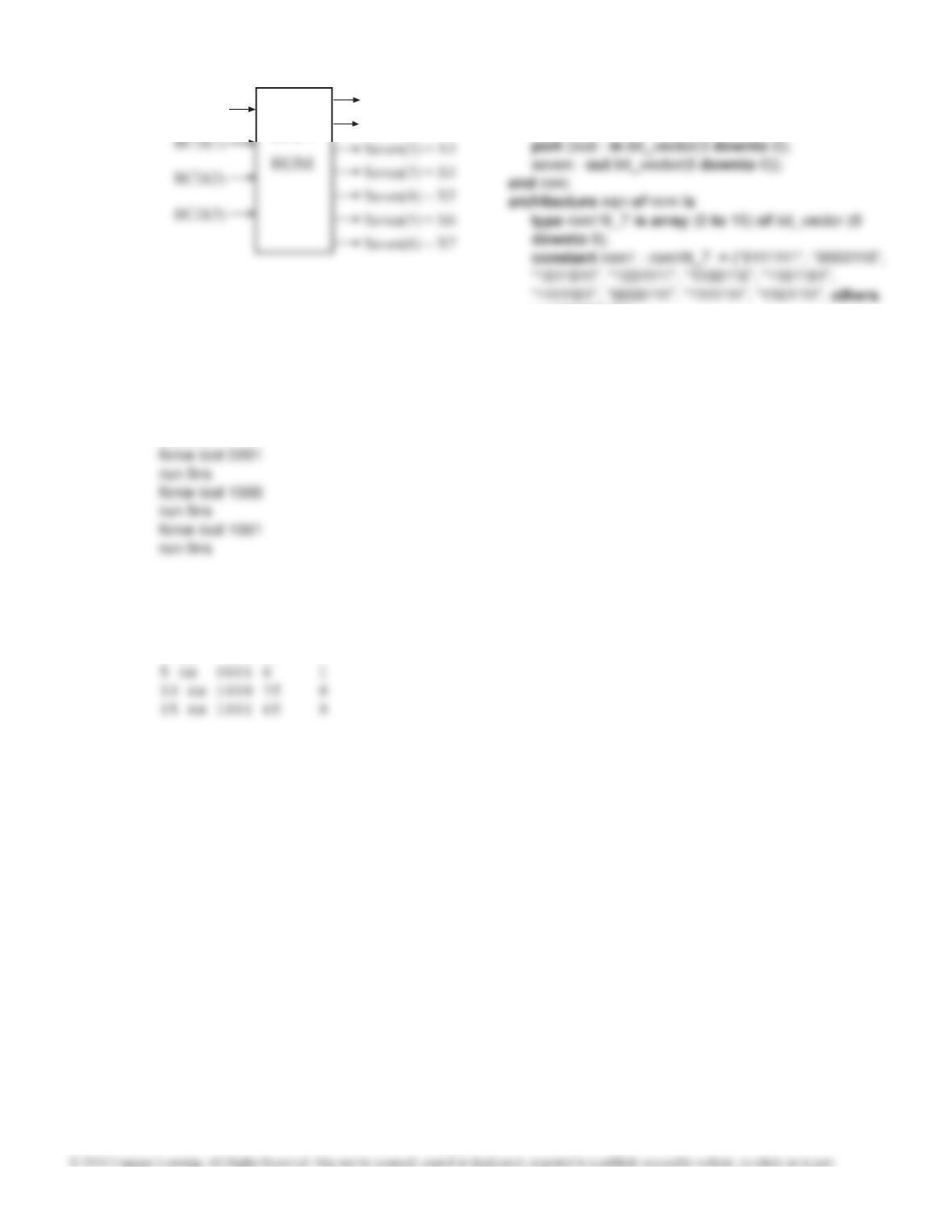
Unit 10 Design Solutions
10.G x
y
x
bin
y
bin
bout
x
y
bin
D
‘
‘
2
X
3
D
2
D
1
D
0
D
3
b
2
b
1
b
in
b
3
X
3
Y
out
b
2
Y
1
X
1
Y
0
X
0
Y
FS3 FS2 FS1 FS0
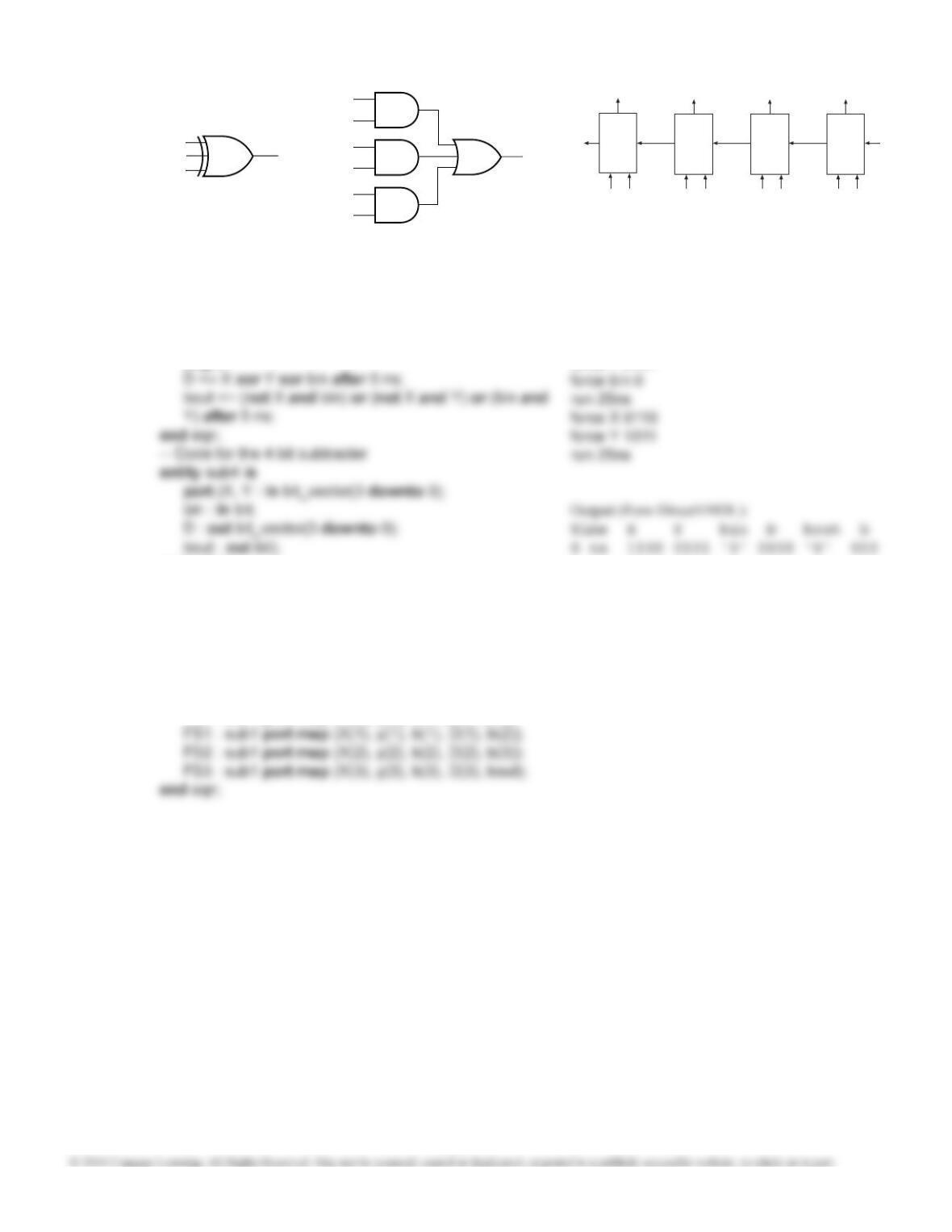
— Code for the full subtracter
entity sub1 is
port (X, Y, bin : in bit;
D, bout : out bit);
end sub1;
architecture eqn of sub1 is
begin
end sub4;
architecture eqn of sub4 is
component sub1 is
port (X, Y, bin : in bit;
D, bout : out bit);
end component;
signal b : bit_vector(3 downto 1);
begin
FS0 : sub1 port map (X(0), y(0), bin, D(0), b(1));
Command Sequence:
force X 1100
force Y 0101
5 ns 1100 0101 ‘0’ 1001 ‘0’ 001
10 ns 1100 0101 ‘0’ 1011 ‘0’ 011
15 ns 1100 0101 ‘0’ 1111 ‘0’ 111
20 ns 1100 0101 ‘0’ 0111 ‘0’ 111
25 ns 0110 1011 ‘0’ 0111 ‘0’ 111
30 ns 0110 1011 ‘0’ 0011 ‘1’ 011
35 ns 0110 1011 ‘0’ 1011 ‘1’ 011
Test Sequence: 1100-0101, 0110-1011
289
Unit 10 Design Solutions
10.H library IEEE;
use IEEE.STD_LOGIC_1164.ALL;
use IEEE.STD_LOGIC_ARITH.ALL;
use IEEE.STD_LOGIC_UNSIGNED.ALL;
entity shifter is
port (Rin : in std_logic;
A : in std_logic_vector(7 downto 0);
B : out std_logic_vector(7 downto 0);
entity mult3 is
port (C : in std_logic_vector(7 downto 0);
D : out std_logic_vector(10 downto 0));
end mult3;
architecture Behavioral of mult3 is
component shifter
port (Rin : in std_logic;
A : in std_logic_vector(7 downto 0);
B : out std_logic_vector(7 downto 0);
end Behavioral;
Test Sequence: C = 10100101, 11111111
Command Sequence:
force C 10100101
Output (from DirectVHDL):
Time C D F E L2 L1
10-bit Adder
C
Sum=D(9 downto 0)
C =D(10)
out
D
11
290
Unit 10 Design Solutions
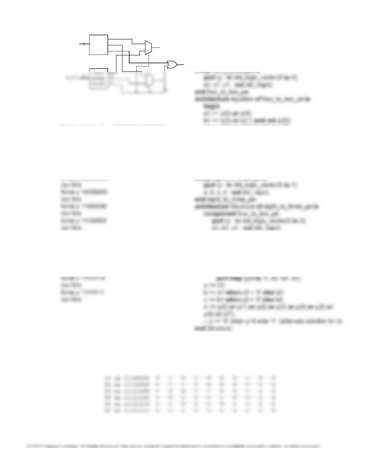
10.I
Y(0:3)
4-to-2
priority
encoder
a
b
c
a
1
1
1
b
d
4
— Code for the 4 to 2 priority encoder
library IEEE;
use IEEE.STD_LOGIC_1164.ALL;
use IEEE.STD_LOGIC_ARITH.ALL;
use IEEE.STD_LOGIC_UNSIGNED.ALL;
c1 <= y(0) or y(1) or y(2) or y(3);
end equation;
library IEEE;
use IEEE.STD_LOGIC_1164.ALL;
use IEEE.STD_LOGIC_ARITH.ALL;
use IEEE.STD_LOGIC_UNSIGNED.ALL;
— Code for the 8 to 3 priority encoder
end component;
signal a1, b1, c1, a2, b2, c2 : std_logic;
begin
four_to_two_pe1 : four_to_two_pe
port map (y(0 to 3), a1, b1, c1);
four_to_two_pe2 : four_to_two_pe
Test Sequence: Y = 00000000, 10000000,
11000000, … , 11111111
Command Sequence:
force y 11110000
run 5ns
force y 11111000
run 5ns
force y 11111100
run 5ns
Output (from DirectVHDL):
Time y a b c d c2 b2 a2 c1 b1 a1
0 ns 00000000 ‘0’ ‘0’ ‘0’ ‘0’ ‘0’ ‘0’ ‘0’ ‘0’ ‘0’ ‘0’
5 ns 10000000 ‘0’ ‘0’ ‘0’ ‘1’ ‘0’ ‘0’ ‘0’ ‘1’ ‘0’ ‘0’
10 ns 11000000 ‘0’ ‘0’ ‘1’ ‘1’ ‘0’ ‘0’ ‘0’ ‘1’ ‘1’ ‘0’
291
Unit 10 Design Solutions
10.J
4-bit
4-bit
D(7:4) D(3:0)
bout cout
library IEEE;
use IEEE.STD_LOGIC_1164.ALL;
use IEEE.STD_LOGIC_ARITH.ALL;
use IEEE.STD_LOGIC_UNSIGNED.ALL;
entity adder4 is
port (X, Y : in std_logic_vector(3 downto 0);
cout <= sum(4);
end addeqn;
Command Sequence:
force A 11011011
force B 01110110
run 10ns
Output (from DirectVHDL):
Time A B D bout bout1 b1 notB D2 D1
0 ns 11011011 01110110 01100101 ‘0’ ‘1’ ‘1’ 10001001 0101 0110
library IEEE;
use IEEE.STD_LOGIC_1164.ALL;
use IEEE.STD_LOGIC_ARITH.ALL;
use IEEE.STD_LOGIC_UNSIGNED.ALL;
entity subtracter8 is
port(A, B : in std_logic_vector(7 downto 0);
end component;
signal b1, cout : std_logic;
signal notB : std_logic_vector(7 downto 0);
signal D1, D2 : std_logic_vector(3 downto 0);
begin
292
Unit 10 Design Solutions
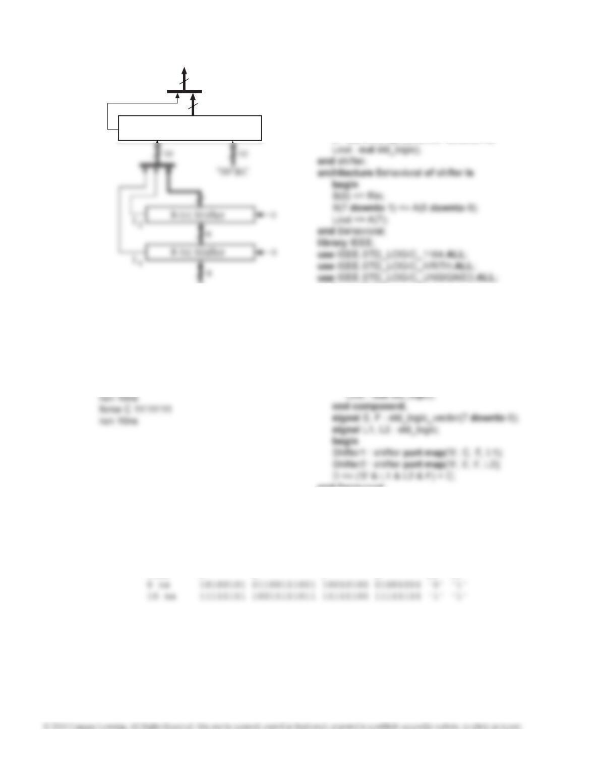
10.K
A
6
library IEEE;
use IEEE.STD_LOGIC_1164.ALL;
use IEEE.STD_LOGIC_ARITH.ALL;
use IEEE.STD_LOGIC_UNSIGNED.ALL;
entity tsb is
Test Sequence: s1 s2 = 00, 01, 10, 11
Command Sequence:
force a 000111
force b 101010
Output (from DirectVHDL):
Time A B C D E s1 s2 internal
0 ns 000111 101010 111000 010101 000111 ‘0’ ‘0’ 0001
library IEEE;
use IEEE.STD_LOGIC_1164.ALL;
use IEEE.STD_LOGIC_ARITH.ALL;
use IEEE.STD_LOGIC_UNSIGNED.ALL;
entity pkc is
end component;
signal internal : std_logic_vector (3 downto 0);
begin
internal(0) <= ‘1’ when (s1 = ‘0’ and s2=’0′) else ‘0’;
internal(1) <= ‘1’ when (s1 = ‘0’ and s2=’1′) else ‘0’;
internal(2) <= ‘1’ when (s1 = ‘1’ and s2=’0′) else ‘0’;
internal(3) <= ‘1’ when (s1 = ‘1’ and s2=’1′) else ‘0’;
tsb0 : tsb port map(A, internal(0), E);
tsb1 : tsb port map(B, internal(1), E);
tsb2 : tsb port map(C, internal(2), E);
tsb3 : tsb port map(D, internal(3), E);
end Behavioral;
293
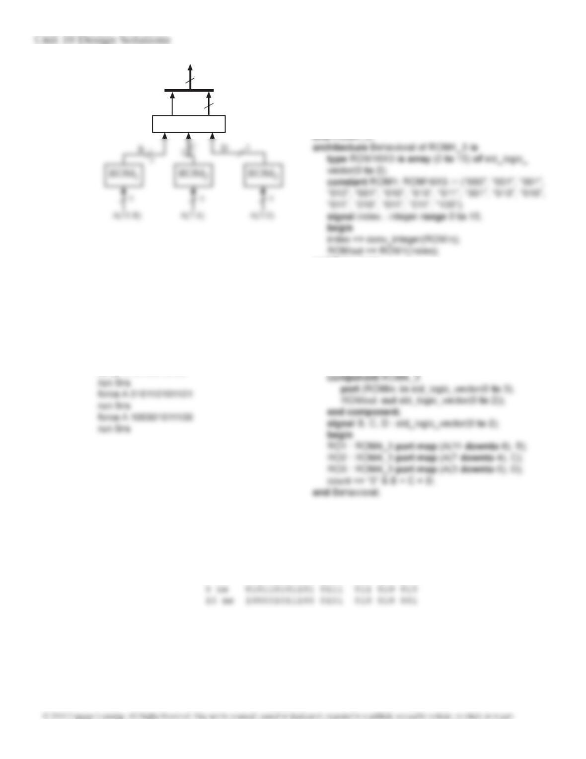
10.L
3-bit adder
Sum
3
4
Count
c
out
library IEEE;
use IEEE.STD_LOGIC_1164.ALL;
use IEEE.STD_LOGIC_ARITH.ALL;
use IEEE.STD_LOGIC_UNSIGNED.ALL;
entity ROM4_3 is
port (ROMin : in std_logic_vector(0 to 3);
ROMout : out std_logic_vector(0 to 2));
end Behavioral;
library IEEE;
use IEEE.STD_LOGIC_1164.ALL;
use IEEE.STD_LOGIC_ARITH.ALL;
use IEEE.STD_LOGIC_UNSIGNED.ALL;
entity lab10l_soln is
port (A : in std_logic_vector(11 downto 0);
count : out std_logic_vector(3 downto 0));
end lab10l_soln;
architecture Behavioral of lab10l_soln is
Test Sequence: A = 111111111111,
010110101101, 100001011100
Command Sequence:
force A 111111111111
Output (from DirectVHDL):
Time A COUNT D C b
0 ns 111111111111 1100 100 100 100
294
Unit 10 Design Solutions
10.M
M(0) N(0)
Di(0)
M(2) N(2) M(1) N(1)
Full
Subtracter
Di(2) Di(1)
b
o
b
i
Full
Subtracter
Full
Subtracter
library bitlib;
use bitlib.bit_pack.all;
entity FSub is
port (X, Y, Bin : in bit;
Bout, Dout : out bit);
end FSub;
architecture Behavioral of FSub is
type ROM8x2 is array ( 0 to 7 ) of bit_vector(0 to 1 );
constant ROM1 : ROM8x2 := (“00”, “11”, “11”, “10”,
“01”, “00”, “00”, “11”);
Dout <= F(0);
end Behavioral;
library bitlib;
use bitlib.bit_pack.all;
entity lab10m is
architecture arch of lab10m is
component FSub
port (X, Y, Bin : in bit;
Bout, Dout : out bit);
end component;
Test Sequence: 110-010 w/ borrow input of 1,
011-101 w/ borrow input of 0
Command Sequence:
force M 110
force N 010
force BI 1
run 5ns
force M 011
force N 101
force BI 0
run 5ns
Output (from DirectVHDL):
Time M N BI BO DI C
295
Unit 10 Design Solutions
10.N
Y(4:7)
4-to-2
priority
encoder
a
b
c
2
2
2
a
b
4
main_enable En1
Test Sequence: Y = 00000000, 10000000,
11000000, …, 11111111
Command Sequence:
force main_enable 1
force y 00000000
run 5ns
force y 11110000
run 5ns
force y 11111000
run 5ns
force y 11111100
run 5ns
force y 11111110
run 5ns
force y 11111111
Output (from DirectVHDL):
Time y main_enable a b c d c2 b2 a2 x c1 b1 a1
0 ns 00000000 ‘1’ ‘0’ ‘0’ ‘0’ ‘0’ ‘0’ ‘0’ ‘0’ ‘1’ ‘0’ ‘0’ ‘0’
5 ns 10000000 ‘1’ ‘0’ ‘0’ ‘0’ ‘1’ ‘0’ ‘0’ ‘0’ ‘1’ ‘1’ ‘0’ ‘0’
library IEEE;
use IEEE.STD_LOGIC_1164.ALL;
begin
a1 <= enable and (y(2) or y(3));
b1 <= enable and (y(3) or (y(1) and not y(2)));
c1 <= enable and (y(0) or y(1) or y(2) or y(3));
end fourtwoarch;
library IEEE;
use IEEE.STD_LOGIC_1164.ALL;
end component;
signal a1,b1,c1,x,a2,b2,c2: std_logic;
begin
x <= not c2;
ENCA: fourtwoencoder port map(y(0 to
3),x,a1,b1,c1);
ENCB: fourtwoencoder port map(y(4 to 7),
main_enable,a2,b2,c2);

296
Unit 10 Design Solutions