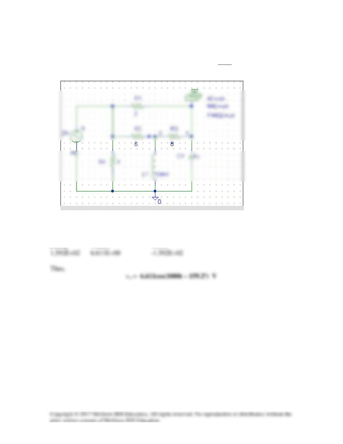
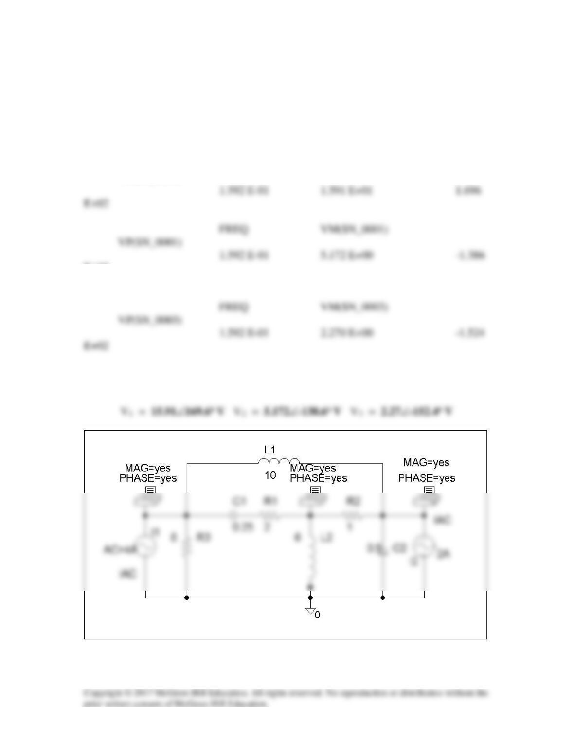
Solution 10.83
The schematic is shown below. The frequency is
15.159
2
1000
2/f =
π
=πω=
When the circuit is saved and simulated, we obtain from the output file
FREQ VM(1) VP(1)
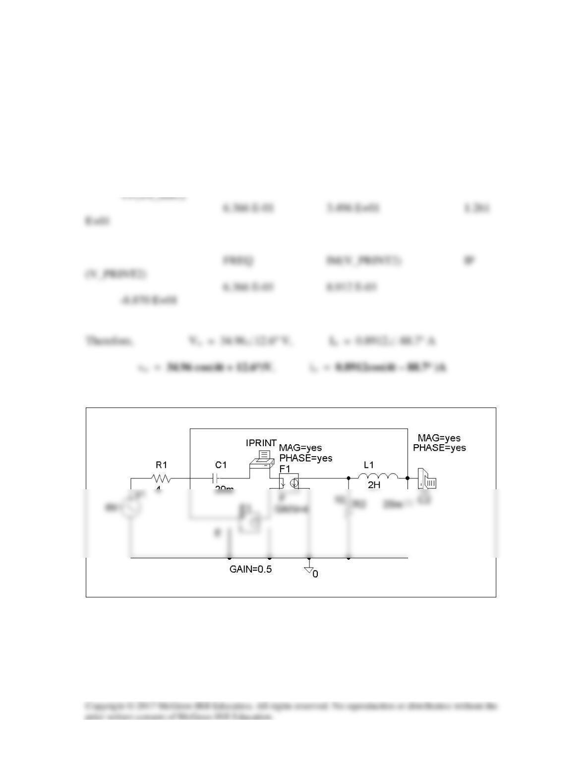
Solution 10.84
The schematic is shown below. We set PRINT to print Vo in the output file. In AC
Solution 10.85
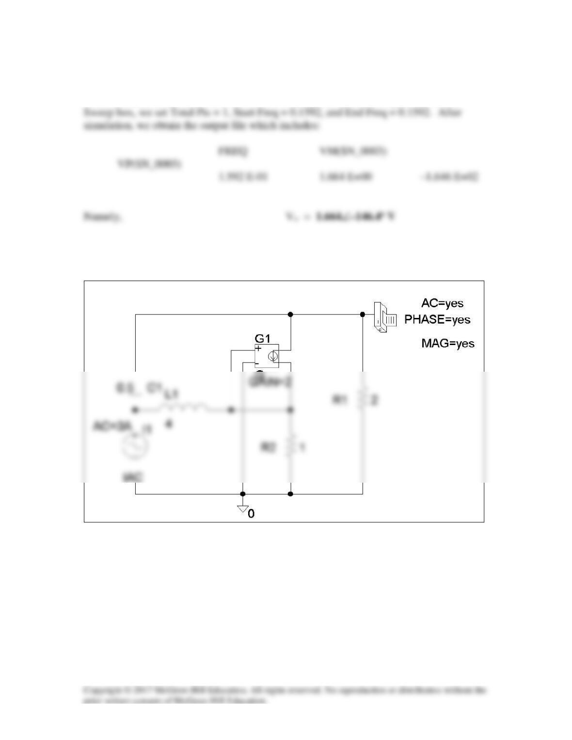
Using Fig. 10.127, design a problem to help other students to better understand
Problem
Use PSpice to find Vo in the circuit of Fig. 10.127. Let R1 = 2 Ω, R2 = 1 Ω, R3 = 1 Ω,
R4 = 2 Ω, Is = 2∠0˚ A, XL = 1 Ω, and XC = 1 Ω.
Solution
The schematic is shown below. We let
1=
ω
rad/s so that L=1H and C=1F.
When the circuit is saved and simulated, we obtain from the output file
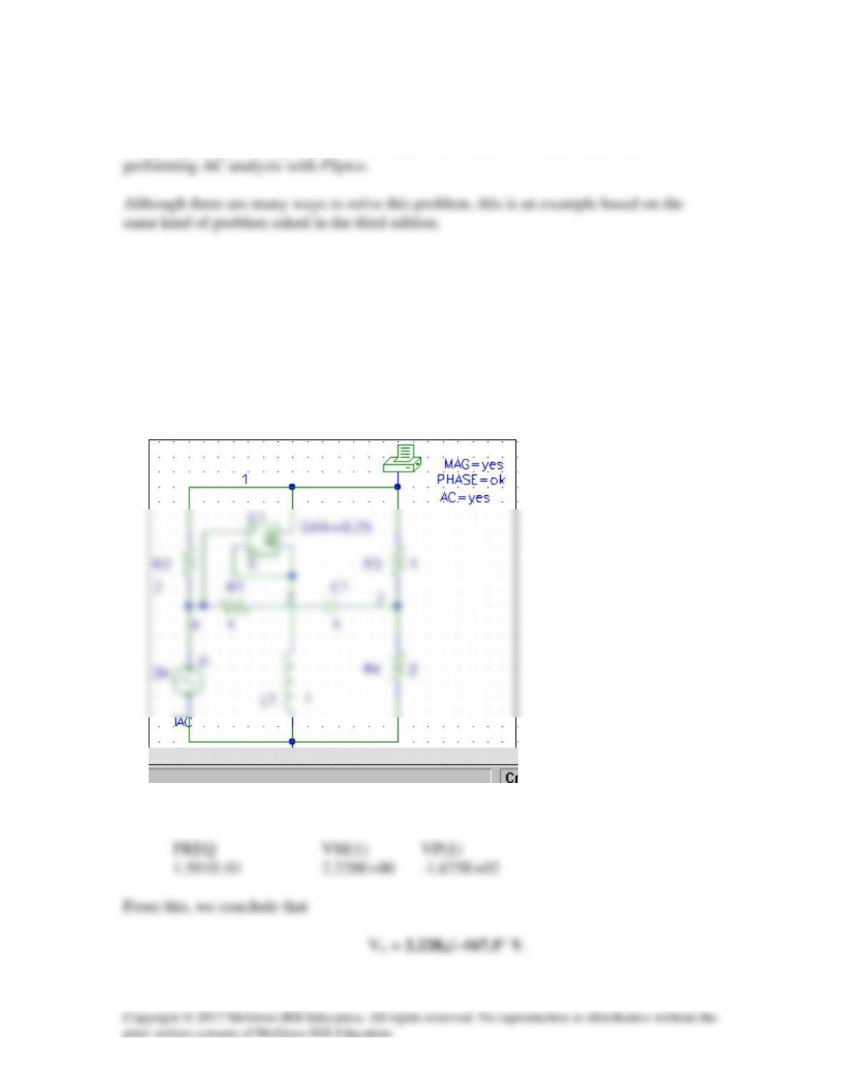
Solution 10.86
The schematic is shown below. We insert three pseudo-component PRINTs at nodes 1,
2, and 3 to print V1, V2, and V3, into the output file. Assume that w = 1, we set Total Pts
= 1, Start Freq = 0.1592, and End Freq = 0.1592. After saving and simulating the circuit,
we obtain the output file which includes:
FREQ VM($N_0002)
VP($N_0002)
Therefore,
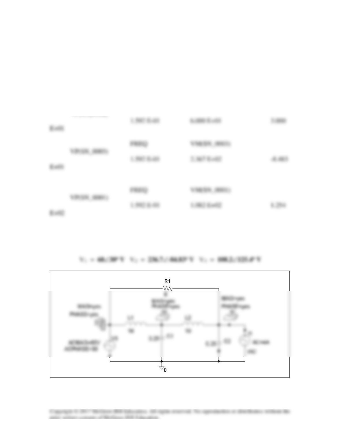
Solution 10.87
The schematic is shown below. We insert three PRINTs at nodes 1, 2, and 3. We set
Total Pts = 1, Start Freq = 0.1592, End Freq = 0.1592 in the AC Sweep box. After
simulation, the output file includes:
FREQ VM($N_0004)
VP($N_0004)
E+02
Therefore,
Solution 10.88
The schematic is shown below. We insert IPRINT and PRINT to print Io and Vo in the
output file. Since w = 4, f = w/2π = 0.6366, we set Total Pts = 1, Start Freq = 0.6366,
and End Freq = 0.6366 in the AC Sweep box. After simulation, the output file includes:
FREQ VM($N_0002)
Solution 10.89
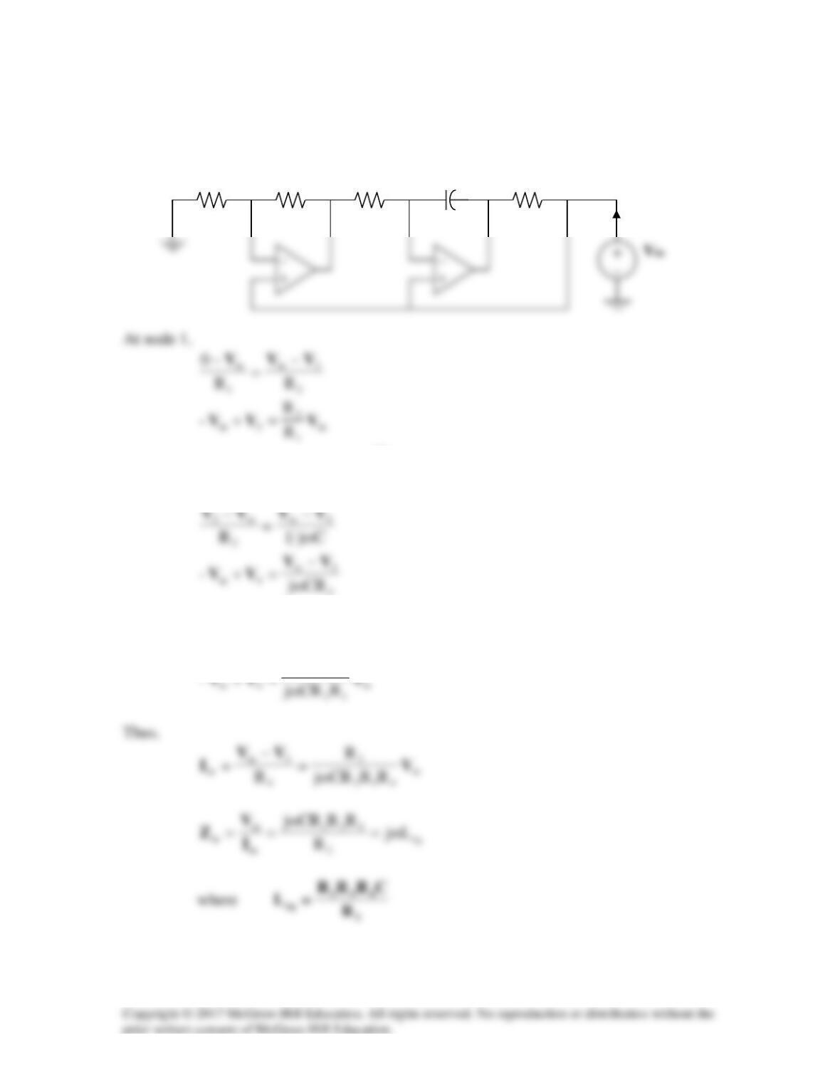
Consider the circuit below.
(1)
At node 3,
(2)
From (1) and (2),
2
R–
C
R1
Iin
R2
R3
R4
Vin
Vin
1
2
3
4
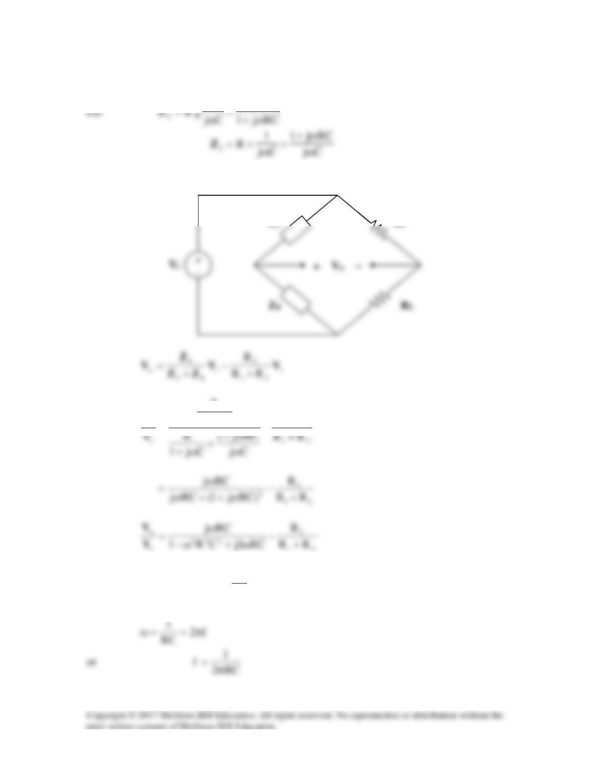
Solution 10.90
R
1
Consider the circuit shown below.
R2
Z4
2
o
R
Cj1
R
−
ω+
=
V
For
o
V
and
i
V
to be in phase,
i
o
V
V
must be purely real. This happens when
0CR1
222
=ω−
R1
Z3
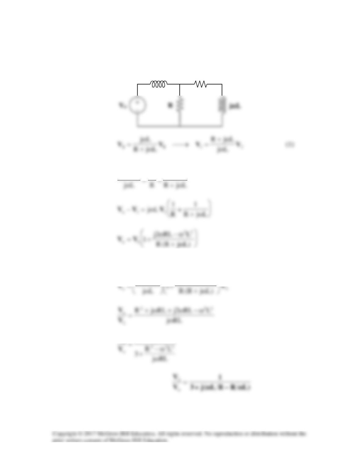
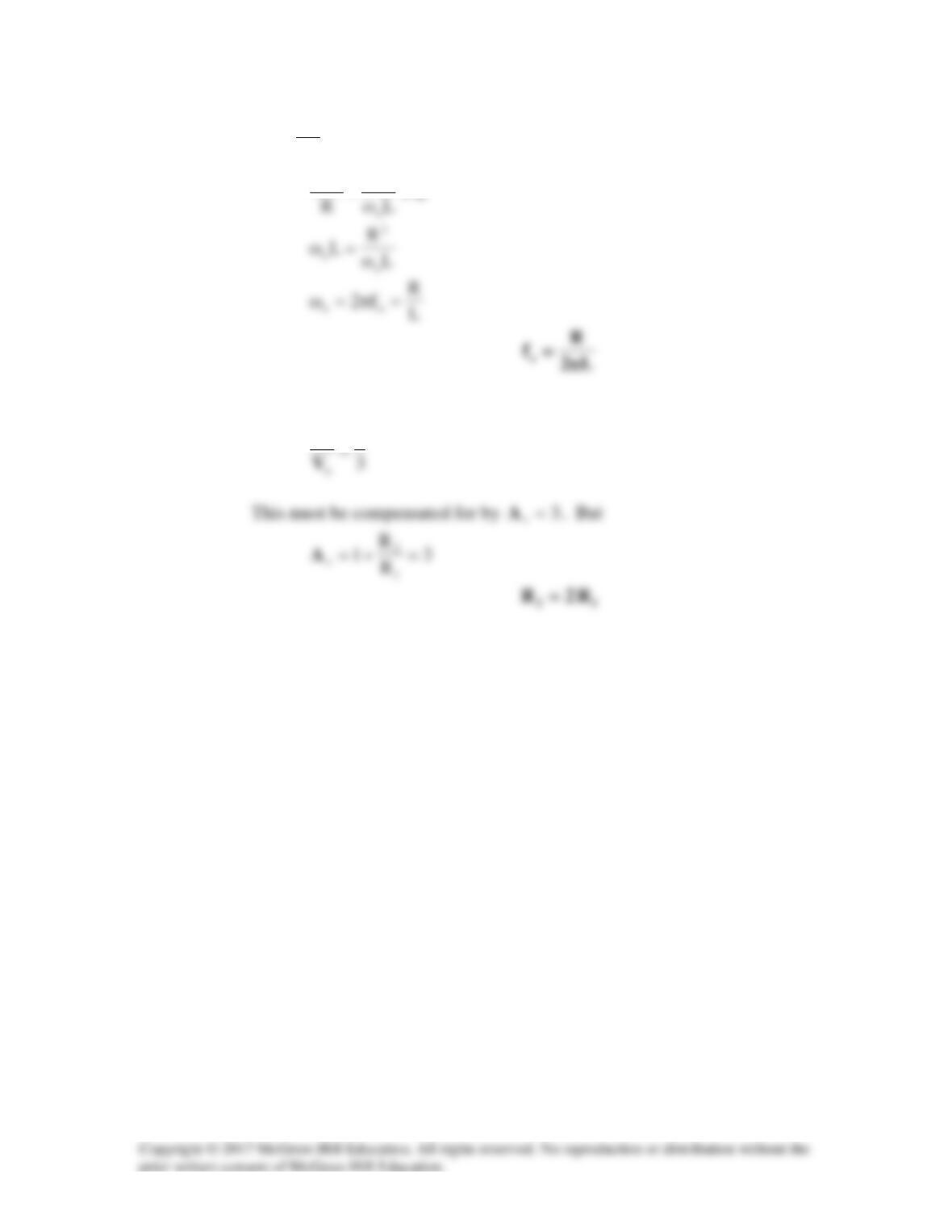
Solution 10.91
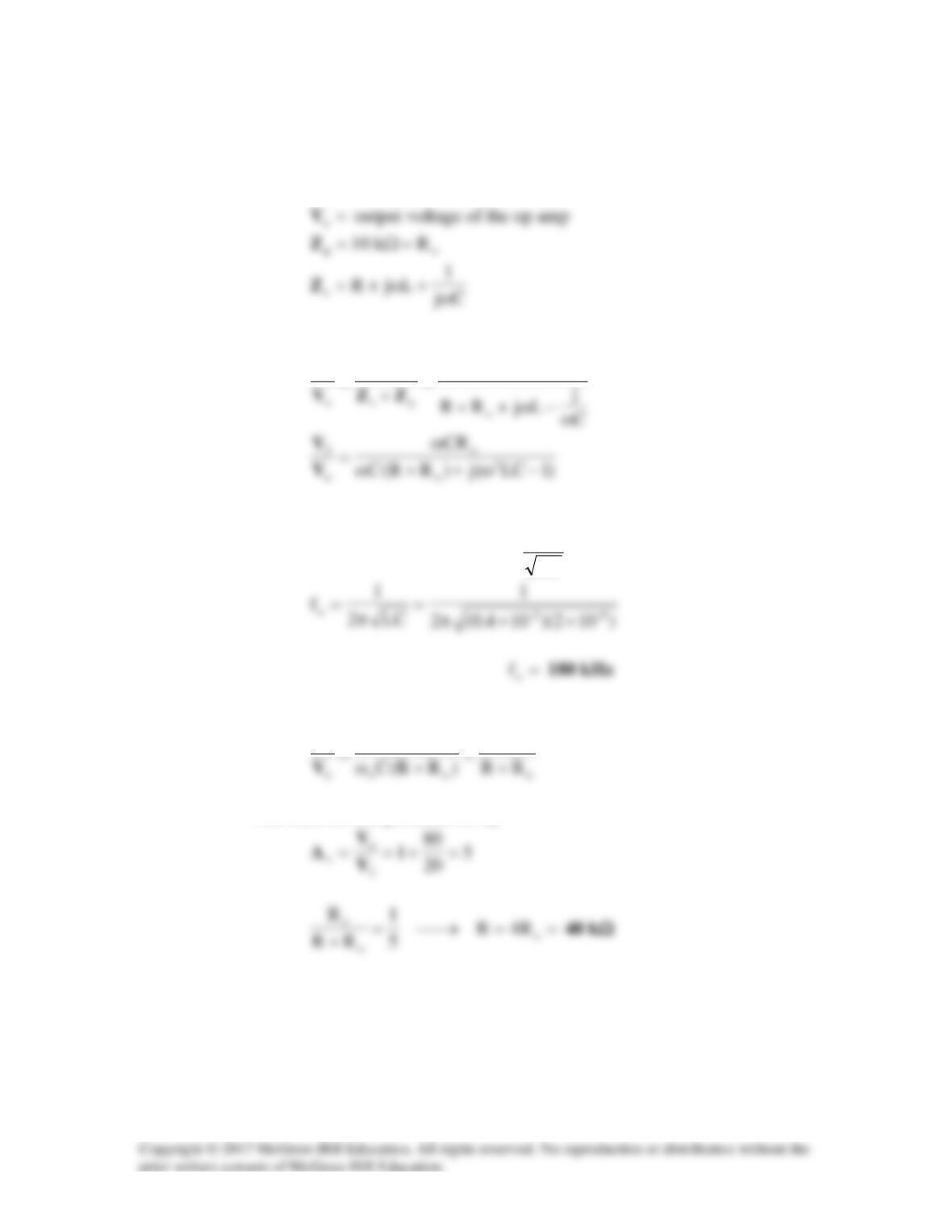
(a) Let
=
2
V
voltage at the noninverting terminal of the op amp
As in Section 10.9,
R
o
p
2
Z
V
For this to be purely real,
LC
1
01LC o
2
o=ω→=−ω
(b) At oscillation,
o
oo
2
R
CR
ω
V
This must be compensated for by
Solution 10.92
Let
=
2
V
voltage at the noninverting terminal of the op amp
As in Section 10.9,
)1LC(jRL
RL
2
p
2
−ω+ω
ω
Z
V
For this to be purely real,
LC2
1
f1LC
o
2
o
π
=→=ω
(a) At
o
ω=ω
,
o
2
R
RL
ω
V
This must be compensated for by
Hence,
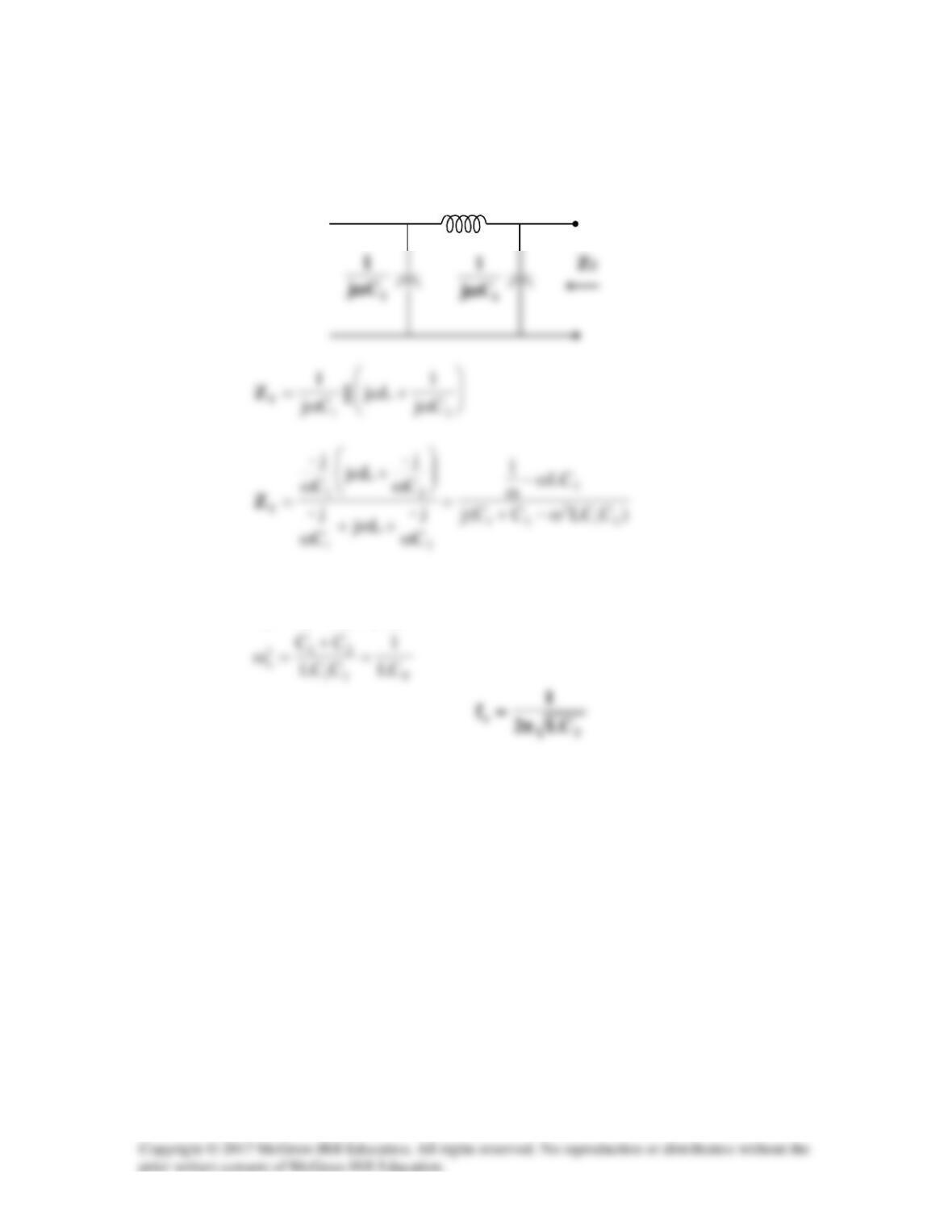
Solution 10.93
As shown below, the impedance of the feedback is
In order for
T
Z
to be real, the imaginary term must be zero; i.e.
0CLCCC 21
2
o21 =ω−+
jωL
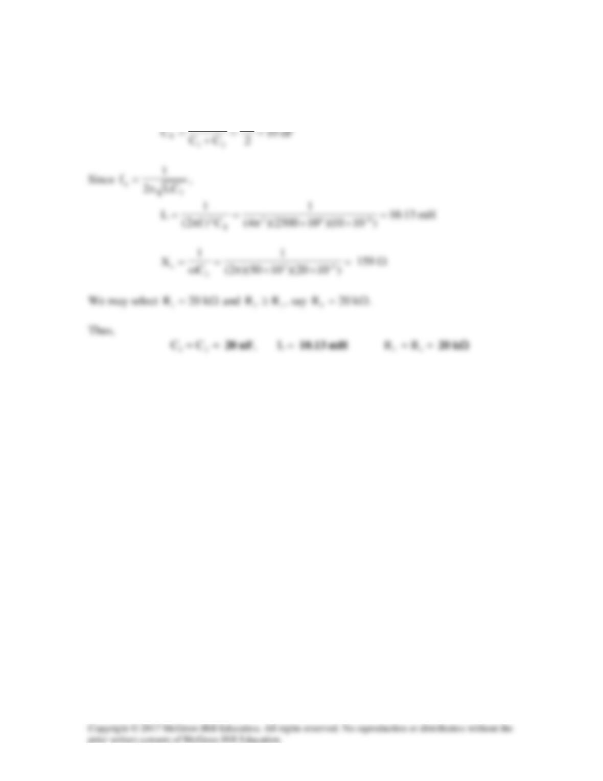
Solution 10.94
If we select
nF20CC
21
==
C
CC
21
Solution 10.95
First, we find the feedback impedance.
In order for
T
Z
to be real, the imaginary term must be zero; i.e.
01)LL(C 21
2
o=−+ω
C
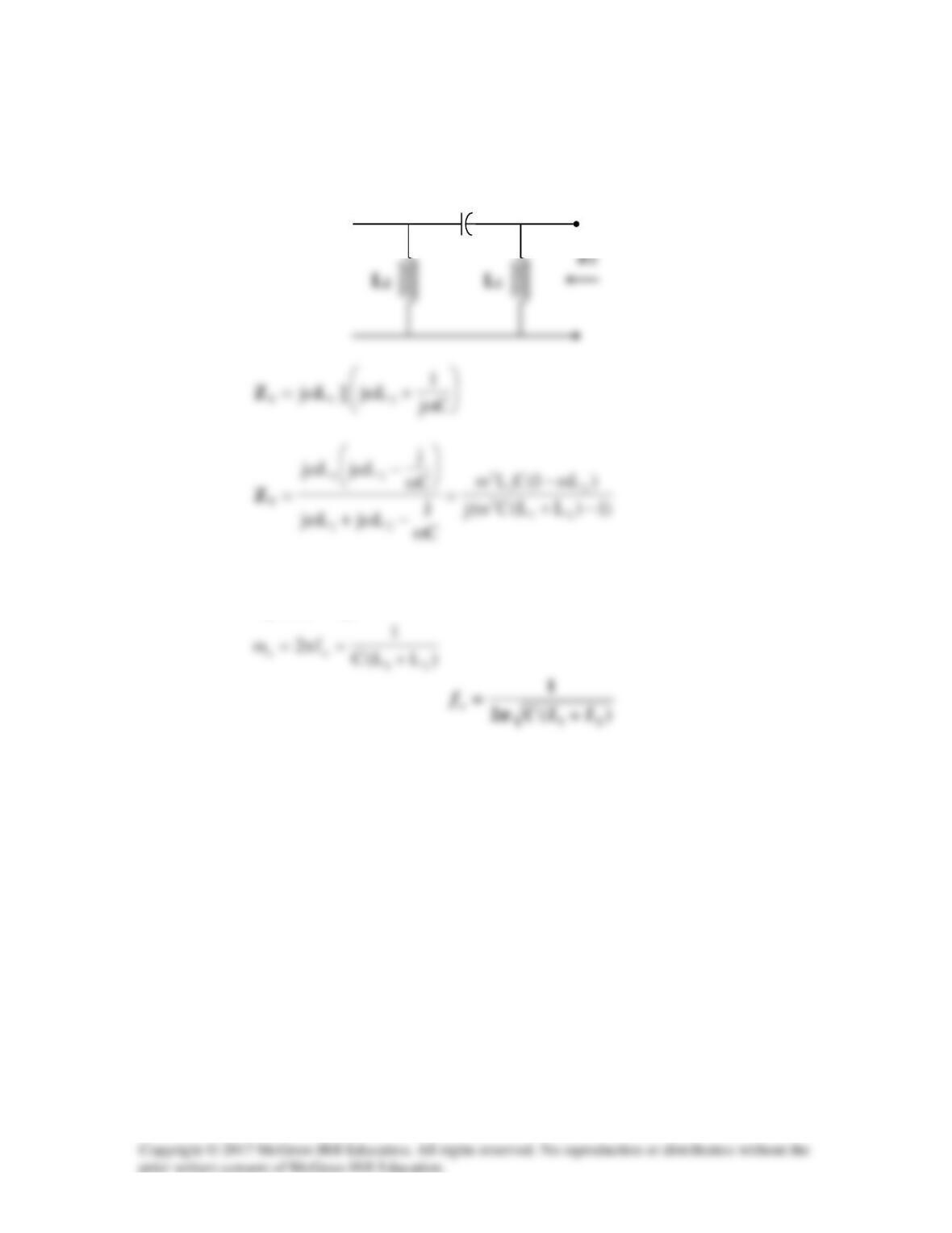
Solution 10.96
(a) Consider the feedback portion of the circuit, as shown below.
Applying KCL at node 1,
11
1o
−VV
VV
(2)
From (1) and (2),
22
LRL2j
LjR VV
ω−ω
ω+
1
2
V
R
V1
V2
jωL
(b) Since the ratio
o
2
V
V
must be real,
R
L
o
ω
(c) When
o
ω=ω
1
2
V