Unlock document.
This document is partially blurred.
Unlock all pages and 1 million more documents.
Get Access
NAME PASSWORD DATE
(signature)
READINESS TEST - UNIT 1 - FORM A
Please answer the following questions carefully without any reference to outside notes. Check your an-
swers before you turn in your paper since an essentially perfect score is required before you go on to the
next unit.
1. Multiply in binary: 11011
× 1011
4. If possible, construct an 1-4-2-3 weighted code for decimal digits. If not possible, explain why. If
possible, express 673 decimal in 1-4-2-3 code.
IV. SAMPLE UNIT TESTS
352
NAME_______________________________PASSWORD__________DATE______________
(signature)
READINESS TEST - UNIT 2R - FORM A
(Issue a theorem sheet with this test)
1. Using a truth table, prove that
(XY)(X′ + Z′) = XYZ′
2. Simplify each of the following expressions
(A′C + B′ + DF′)[A + C′ + B′ + DF′] =
3. Factor as much as possible: (Your answer should be in product-of-sums form)
Z + XYQ + XYP =

NAME______________________________ PASSWORD___________ DATE____________
(signature)
READINESS TEST - UNIT 3R - FORM A
1. Is the following statement always true? Justify your answer.
3. Each time you apply a theorem, mark your paper clearly to indicate which terms were used to add or delete
4. Simplify to obtain a sum of 3 terms:
(A ≡ B’)(CD ⊕ B’) + ABCD

354
NAME PASSWORD DATE
(signature)
READINESS TEST - UNIT 4 - FORM A
1. A switching circuit has three inputs (A, B, C) and one output (Z). If A= 0, the output Z is the
exclusive-OR of B and C. If A = 1, the output is the equivalence of B and C.
2. Without using a truth table, find (a) the minterm and maxterm expansions for F in algebraic and
3. Write an equation for the following sequence (use only 3 variables for the right-hand side) : The
4. Design a 4-bit adder/subtracter using four full adders and four exclusive-OR gates. When Su = 1, the
circuit should output A - B, otherwise it should output A + B. Remember that B' = B ⊕ 1. (Assume
that negative numbers are represented in 2’s complement).
355
NAME _______________________________ PASSWORD _________ DATE __________
(signature)
READINESS TEST - UNIT 5R - FORM A*
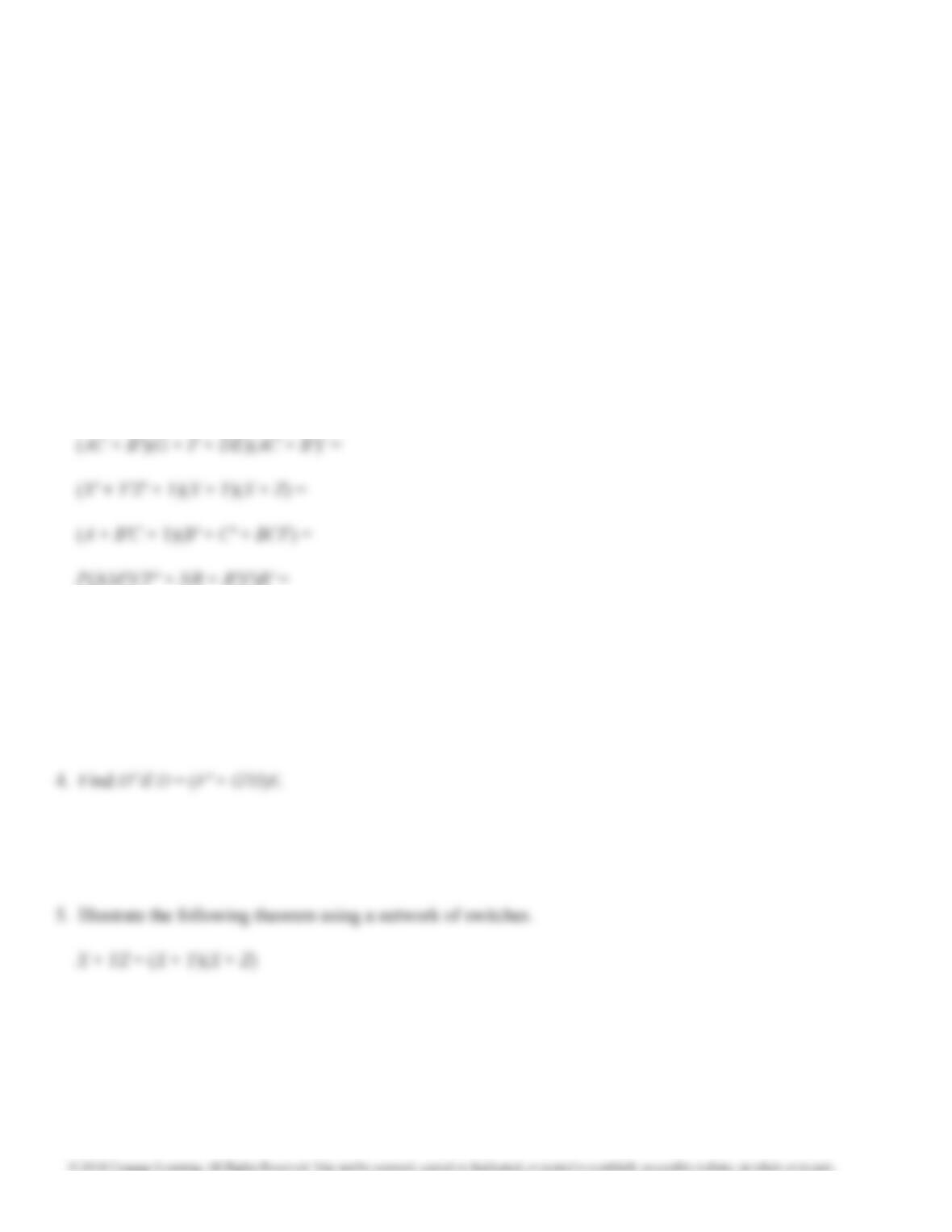
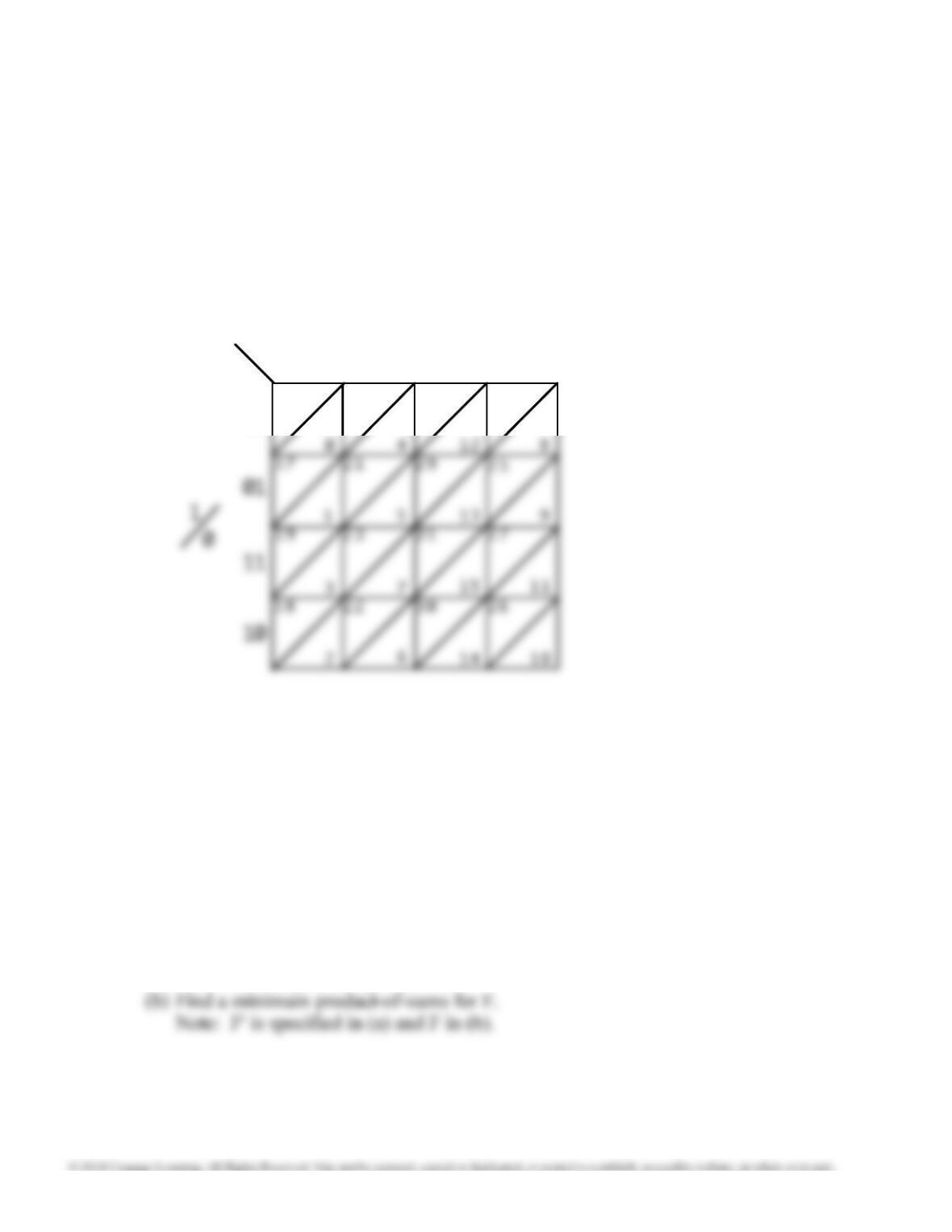
1. F(a, b, c, d, e) = Σ m(0, 1, 2, 6, 7, 8, 16, 17, 19, 20, 25, 26, 29, 31) + Σ d(3, 5, 18, 27)
(a) Find the essential prime implicants of F and indicate the minterm which makes each one
essential.
(b) Find a minimum sum-of-products expression for F.
20 28 24
16
00 01
10
00
11
2. F(a, b, c, d) = Σ m(7, 11, 12, 14) + Σ d(0, 10)
(a) Find all of the prime implicants of F'.

NAME PASSWORD DATE
(signature)
READINESS TEST - UNIT 6 - FORM A
1. Find two different minimum sum-of-products expresstions for F using the Quine-McCluskey proce-
dure:
2. What theorem is used when combining terms in the Quine-McCluskey procedure?
3. Find a minimum sum of products for G using a 4-variable Karnaugh map.
G = A'BD' + A'C'D' + A'BDE + ABD'F + AC'D'F

NAME ________________________________ PASSWORD ________DATE __________
(signature)
READINESS TEST - UNIT 7R - FORM A
1. Find a minimum 3-level NOR circuit to realize
2. (a) Design a minimum 2-level NOR-NOR circuit to realize
3. Find a minimum 2 level NAND gate circuit to simultaneously realize
F1(A, B, C, D) = Σ m(1, 3, 5, 7, 8, 9, 13)
358
NAME _______________________________ PASSWORD _________ DATE __________
(signature)
READINESS TEST - UNIT 9R - FORM A*
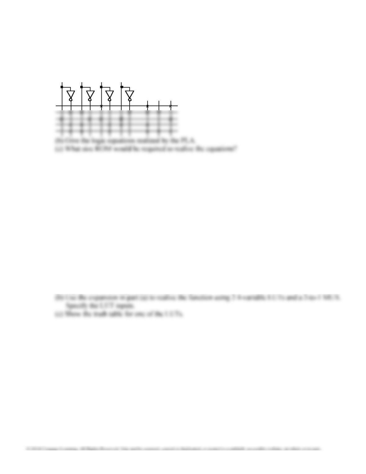
1. (a) Given the following PLA connection diagram, specify the PLA contents in table form.
2. (a) Write the logic equation for the output of an 8-to-1 MUX with control inputs B, C, D.
(b) Implement a 4-to-1 MUX having control inputs A, B using gates.
(c) Implement a 4-to-1 MUX using a 2-to-4 decoder and tri-state
buffers to select one of the decoder
outputs.
3. Z(a,b,c,d,e) = a′b′cd′ + ac′de′ + a′bd′e + bde
(a) Expand the above expression about the variable a.
DB CA
F
1
F
2
F
3
NAME _______________________________ PASSWORD _________ DATE __________
(signature)
READINESS TEST - UNIT R1R - FORM A
TIME LIMIT 60 MINUTES
1. For the following function, find the simplest sum-of-products form algebraically: (Hint: Minimum
2. Find a minimum 2-level multiple output NOR-NOR realization for the two functions given by the
PLA table below. (Hint: Minimum solution has seven gates.)
w
x
y
z
f
1
f
2
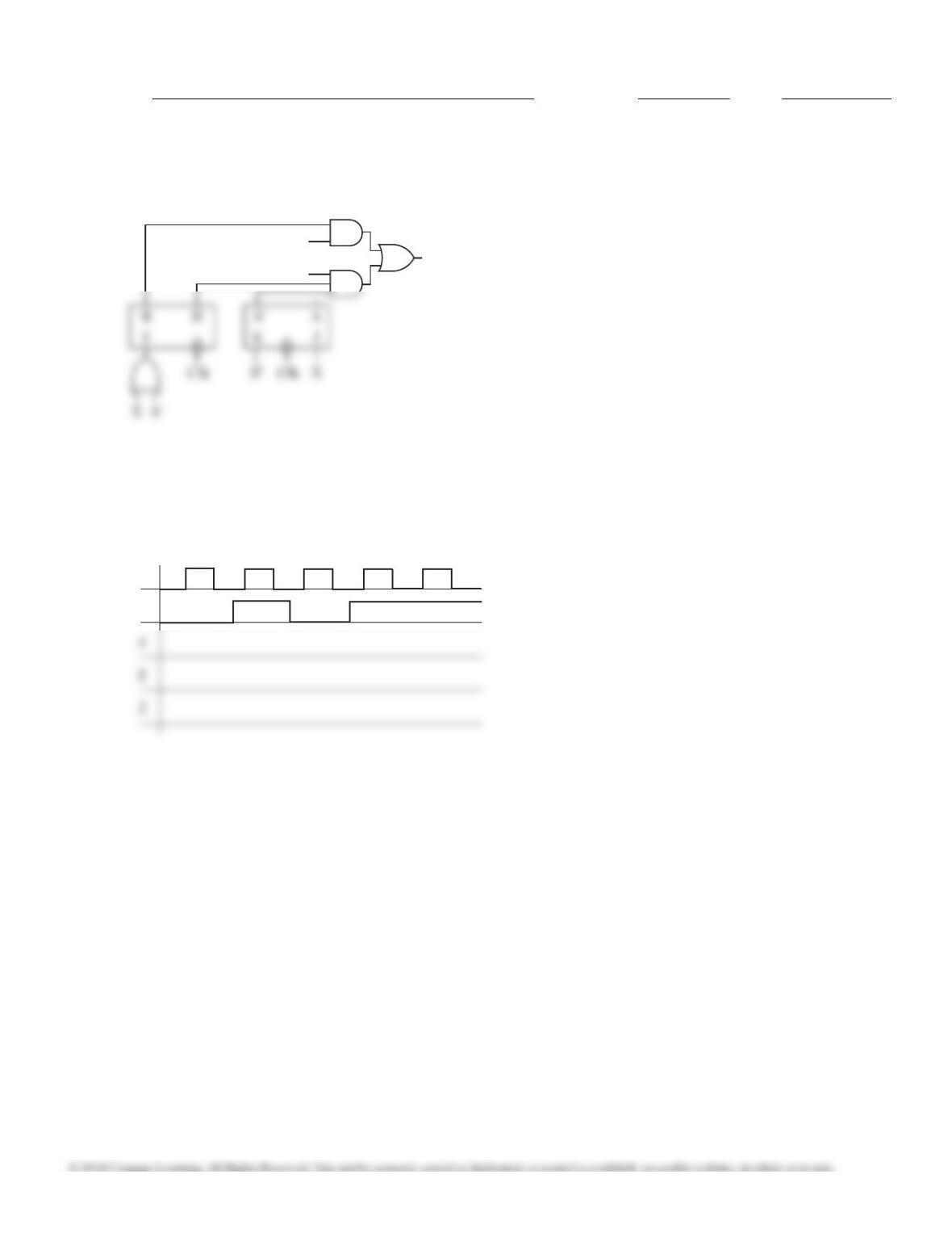
4. B and C are initially zero. Assume 10 ns gate delays and complete the timing diagram below.
A
A
B
NAME_______________________________ PASSWORD____________ DATE__________
(signature)
READINESS TEST - UNIT 10 - FORM A
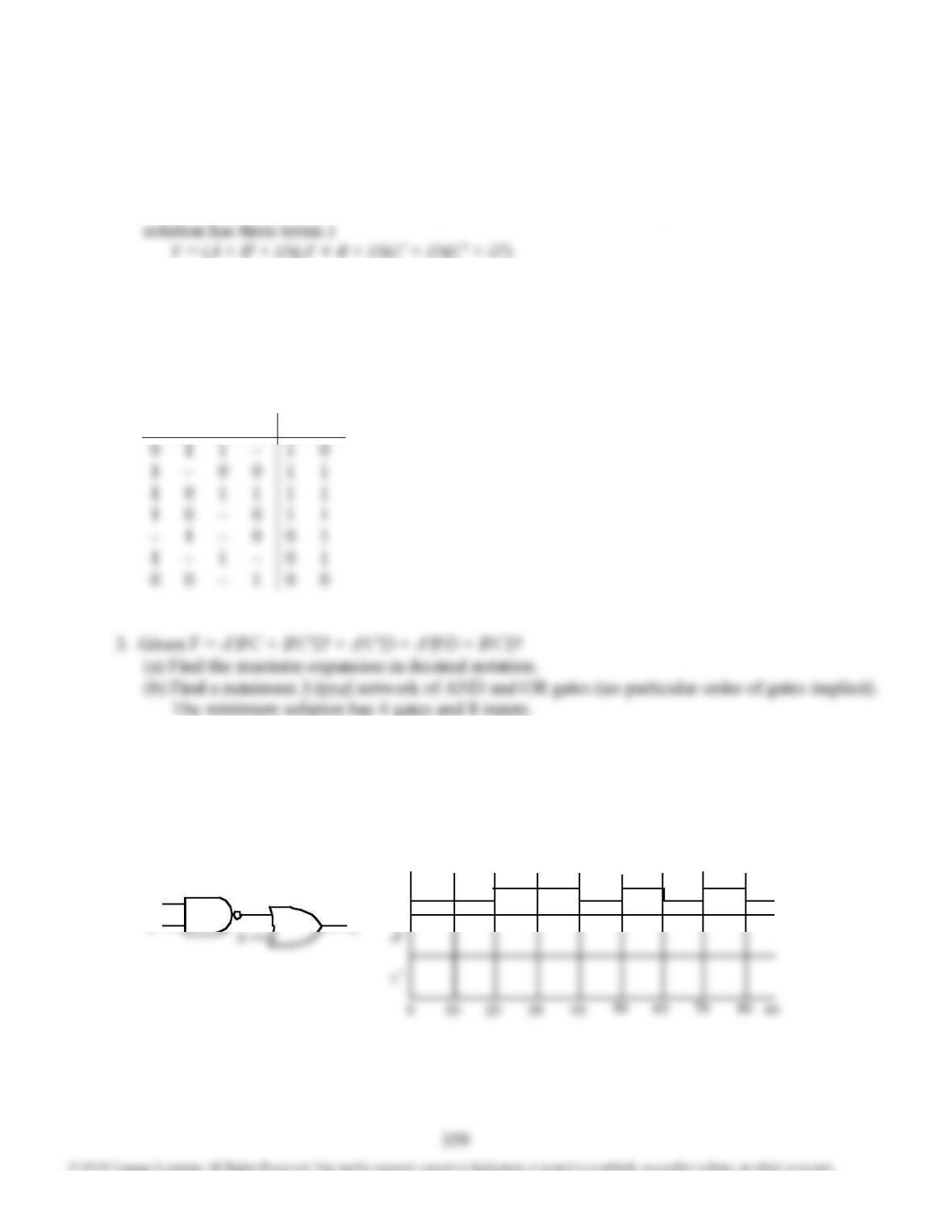
1. Write a conditional signal assignment statement that represents the following network.
2. Draw a network that implements the following VHDL code:
A <= B or not C and not D;
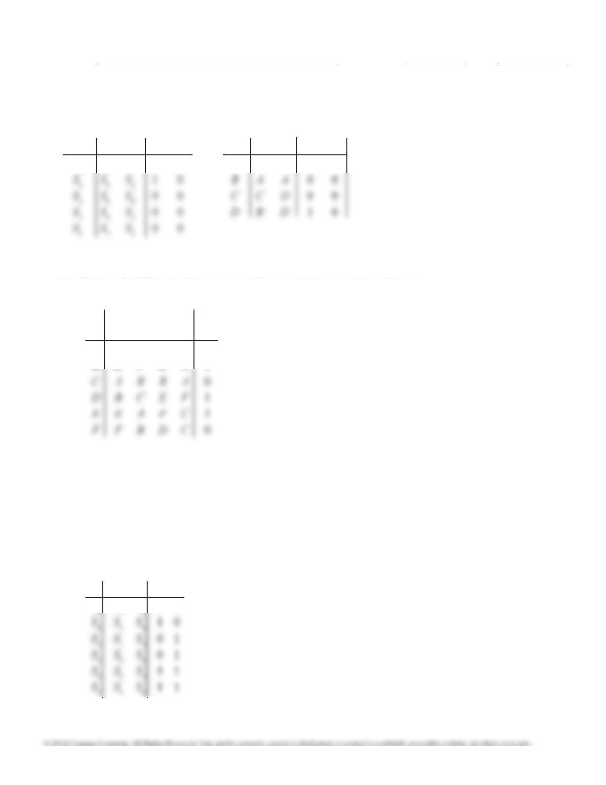
3. A 3-to-8 decoder can be represented by a truth table with inputs X1 X2 X3 and outputs D7 D6 D5 D4 D3
D2 D1 D0. Write a complete VHDL module that implements the decoder using an 8 words X 8 bits
ROM.
4. Evaluate the following expression for A = “010” and B = “110”: (TEST is of type Boolean)
TEST <= (A & B or not (B & A)) < (B & A and not A & A)
0
A
X
1
D
7
NAME_______________________________ PASSWORD____________ DATE__________
(signature)
READINESS TEST - UNIT 11R - FORM A
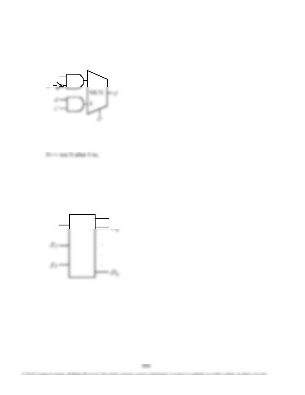
1. An M-N flip-flop behaves as follows:
If MN = 11, the flip-flop is set to Q = 0.
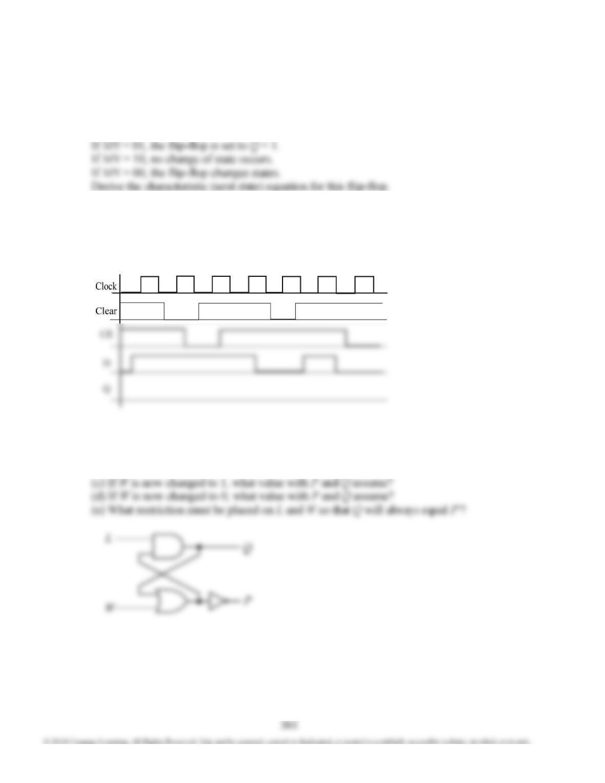
2. Complete the following timing diagram for a rising edge triggered D-CE flip-flop with a clear input.
3. For the latch given below,
(a) If L = W = 0, what value with P and Q assume?
(b) If L is now changed to 1, what value with P and Q assume?
NAME_________________________________ PASSWORD_________ DATE___________
(signature)
READINESS TEST - UNIT 12R - FORM A
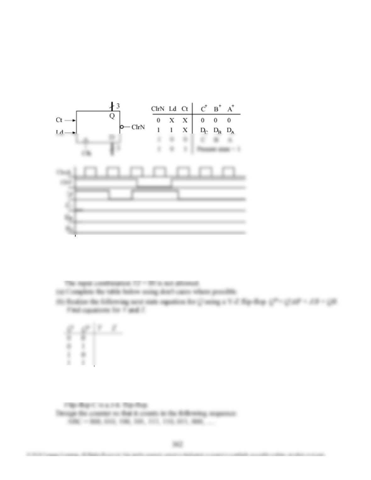
1. Consider the following Loadable Counter with an Asynchronous Clear. Assuming that Count (Ct
) is 1
throughout-and that DCDBDA are 010-complete the timing diagram.
2. A Y-Z flip-flop behaves as follows:
If YZ = 01, the flip-flop does not change state.
If YZ = 11, the flip-flop is set to Q = 1.
If YZ = 10, the flip-flop changes state.
3. A 3-bit counter uses three different types of flip-flops as follows:
Flip-flop A is a D flip-flop.
Flip-flop B is a T flip-flop.
363
NAME PASSWORD DATE
(signature)
READINESS TEST - UNIT 13 - FORM A
1. (a) For the given circuit, construct a transition table and a state graph.
Z
X'
X
(b) Complete the following timing chart. Indicate at what times Z has the correct value and specify
the correct output sequence. Initially A = B = 0.
Clock
X
2. Draw a general model of a Moore circuit with m inputs, n outputs, and k D ip-ops.

NAME PASSWORD DATE
(signature)
READINESS TEST - UNIT 14 - FORM A
1. A Mealy sequential circuit has one input and two outputs. When the fourth input is received, the
circuit outputs Z1 = 1 if the majority of the inputs are 0’s, Z2 = 1 if the majority are 1’s, and Z1 = Z2 =1
2. A Moore circuit has one input and one output. The output is initially zero. The output is the same
as the input just received, unless the input sequence 1011 occurs, in which case the output remains 1
365
NAME PASSWORD DATE
(signature)
READINESS TEST - UNIT 15 - FORM A
1. State tables for circuits N1 and N2 are given below. Are the circuits equivalent? Justify your answer.
N10 1 0 1 N20 1 0 1
S0S3S10 0 A C D 0 0
2. Reduce the following Moore state table to a minimum number of states.
X1 X2
00 01 11 10 Z
A C D D F 0
3. (a) The following state table is to be realized using D ip-ops. Make a suitable state assignment
which will lead to an economical circuit. Assign 000 to S0 and 010 to S2. Show how you arrived
at your state assignment.
(b) For the assignment obtained in (a) derive the input equations for the ip-ops and the output
equation.
0 1 0 1
S0S1S50 0
NAME PASSWORD DATE
(signature)
READINESS TEST - UNIT 17 - FORM A
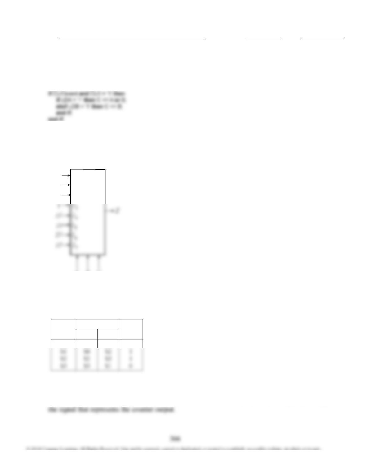
1. Draw a diagram to show the hardware that the following VHDL code represents. Use a D-CE ip-op
and gates.
2. Write a VHDL process using a case statement that represents the following MUX:
A
B
I2
I1
I0
C
1
D
0
3. Write a VHDL code module that implements the following state table. Assume that all state changes
occur on the rising edge of the clock. Use two processes. Use a case statement with if-then-else state-
ments.
Present
State
Next State
Output
X = 0 X = 1
S0
S0
S2
0
4. Write a VHDL process to represent a 4-bit counter that will increment on every falling edge of the
clock. The counter has an asynchronous, active low reset that overrides the clock. Specify the type of
NAME PASSWORD DATE
(signature)
READINESS TEST - UNIT 18 - FORM A
1. This problem concerns the design of a serial adder/subtracter with accumulator for 4-bit numbers as
shown below.
y3y2y1y0
Full
Adder
xin
yin
carry
sum
x3x2x1x0
Control
Circuit
Clock
St
SI
Sh
Sh SI
Sh
0
Combinational
Logic
Circuit
xout
y
out
Clock
(a) Construct a state graph for the control circuit (3 states). The operation should begin when St is set
to 1. St may be 1 for one clock cycle, or it might remain 1 for many clock cycles, even after the
addition is completed. Make sure that the circuit does not begin again after it is finished! The start
signal must be changed back to 0 to reset the control circuit.
(b) Design the control unit using D ip-ops and any kinds of gates.
(c) Design the combinational logic circuit.
2. (a) Draw a block diagram for a parallel divider which is capable of dividing a positive 8-bit binary
number by a positive 4-bit binary number to give a 4-bit quotient. Use a 9-bit dividend register, a
368
NAME PASSWORD DATE
(signature)
READINESS TEST - UNIT 19 - FORM A
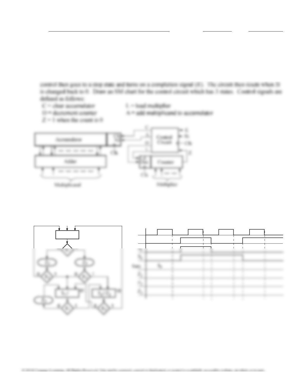
1. This problem concerns the design of a digital system which multiplies two binary numbers by the re-
peated addition method. The block diagram of the system is shown below. When a start signal (St) is
set to 1, the accumulator is cleared and the multiplier is loaded into a counter. The multiplicand is then
added to the accumulator and the counter is decremented until the multiplication is complete. The
2 (a) Realize the following SM chart using a PLA and D ip-ops that trigger on the falling edge of the
clock pulse. Draw a block diagram and give the PLA table. (Do not simplify the equations.)
(b) Complete the timing diagram.
S / Z
0 1
00
Clock
X
1


