Unit 8 Design Solutions
Problems 8.A through 8.S are combinational logic design problems using NAND and NOR gates.
Problems 8.A through 8.R are of approximately equal difficulty so that different students in the
class can be assigned different problems. We ask our students to use the following procedure:
(1) Derive a truth table for the assigned problem.
(2) Use Karnaugh maps to derive logic equations in sum-of-products or product-of-sums form
depending on whether NAND gates or NOR gates are required.
(3) Enter the truth table into LogicAid, derive the logic equations, and check the answers
In Unit 10, we ask our students to implement the same design problem using VHDL, synthesize it
and download it to a CPLD or FPGA on a hardware board that has switches, LEDs, and 7-segment
indicators.
For each design problem, the solutions that follow show a SimUaid circuit that meets the problem
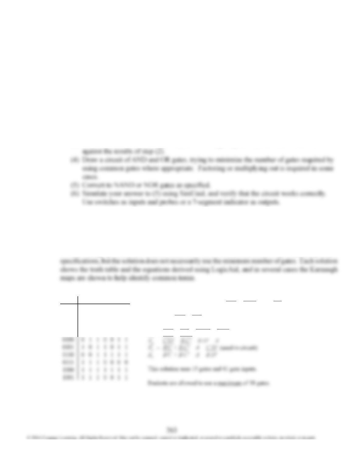
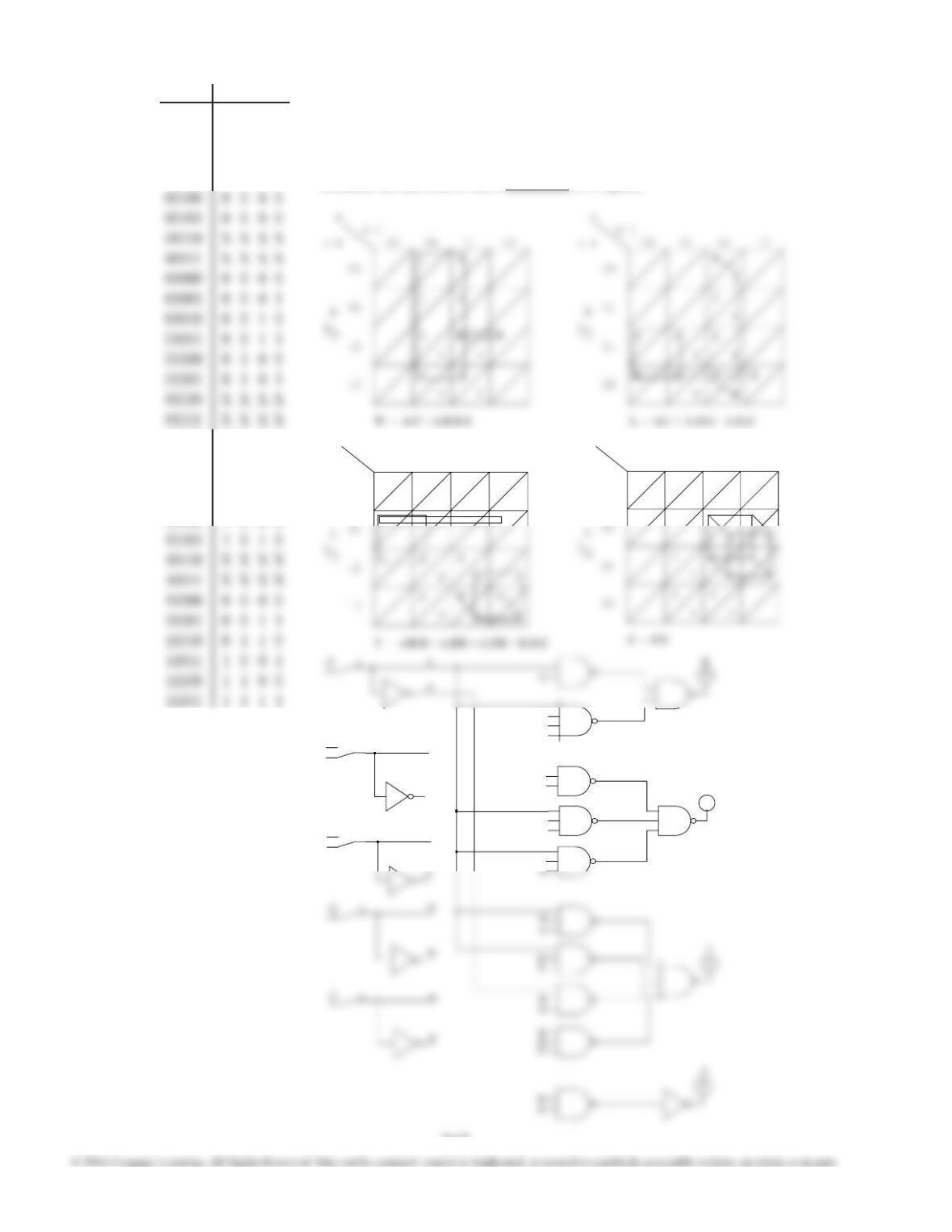
8.A X1 = B’D’ + B D + A + C D = B’D’ + BC’D + A + CD (used in circuit)
X1 = B’D’ + B D + A + B’C
X2 = B’ + C’D’ + C D
X3 = C’ + D + B
X4 = B’D’ + B’C + B C’D + C D’
X5 = B’D’ + C D’
0000 1 1 1 1 1 1 0
0001 0 1 1 0 0 0 0
0010 1 1 0 1 1 0 1
0011 1 1 1 1 0 0 1
ABCD X
1
X
2
X
3
X
4
X
5
X
6
X
7
III. SOLUTIONS TO DESIGN, SIMULATION,
AND LAB EXERCISES
Solutions to Unit 8 Design Problems
Unit 8 Design Solutions
264
X
A B
C D 00 01 11 10
00
01
1
1
1
X
X
4X
A B
C D 00 01 11 10
00
01
1
1
X
X
5
X
A B
C D 00 01 11 10
00
01
1
1
1
1
X
X
7
7
X
A B
C D 00 01 11 10
00
01
1
1
1
1
X
X
1
X
A B
C D 00 01 11 10
00
01
1
1
1
1
1
X
X
2X
A B
C D 00 01 11 10
00
01
1
1
1
1
1
1
X
X
3
8.A
(cont.)
X
A B
C D 00 01 11 10
00
01
1 1
1
1
1
X
X
6
1
00
1
00
A
A’
B
B’
1
D
B’
D’
B
C’
D
BX2
C’
D’
X1
Unit 8 Design Solutions
265
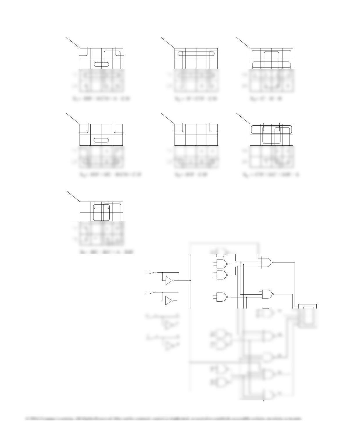
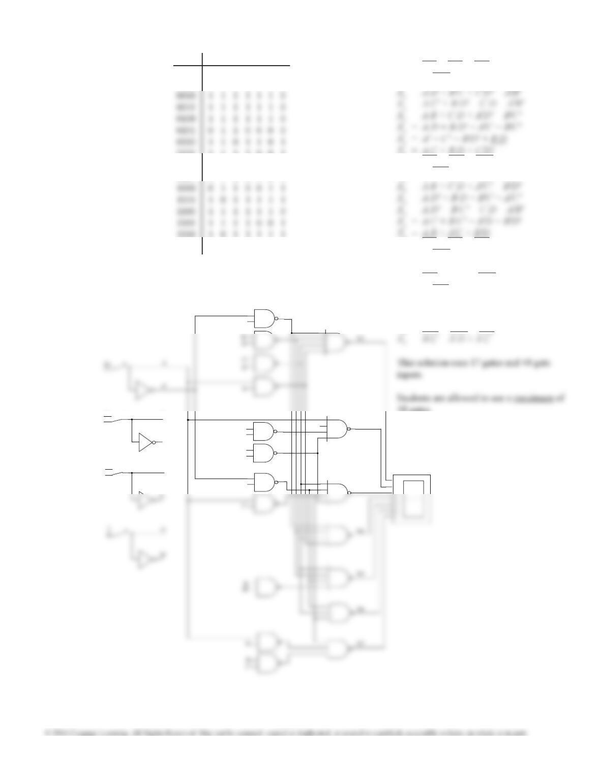
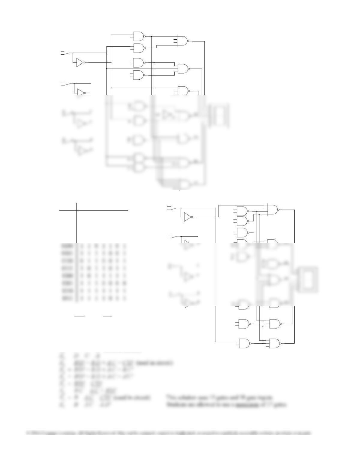
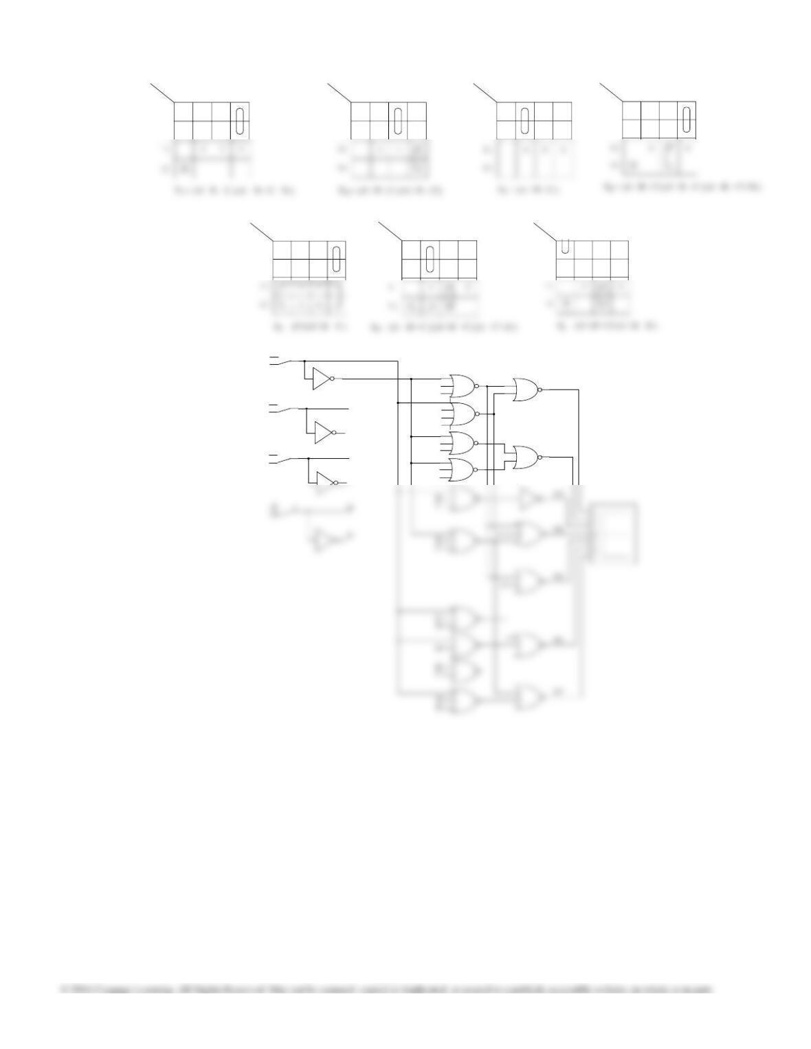
8.B X1 = B’ + C’D + C D’ + A
X2 = C + B
X3 = D’ + C + A (used in circuit)
X3 = D’ + C + B’
X4 = C’D + B’D + B C D’ + A C’ (used in circuit)
BX1
B’
C’
X2
C’
D
X3
C’
D
C
D’
1
00
1
00
A
A’
B
0000 X X X X X X X
0001 X X X X X X X
0010 X X X X X X X
0011 1 1 1 1 1 1 0
ABCD X
1
X
2
X
3
X
4
X
5
X
6
X
7
Unit 8 Design Solutions
266
B’
E’
Z
B’
B’
D’
E’
00
1
00
D’
E
E’
0
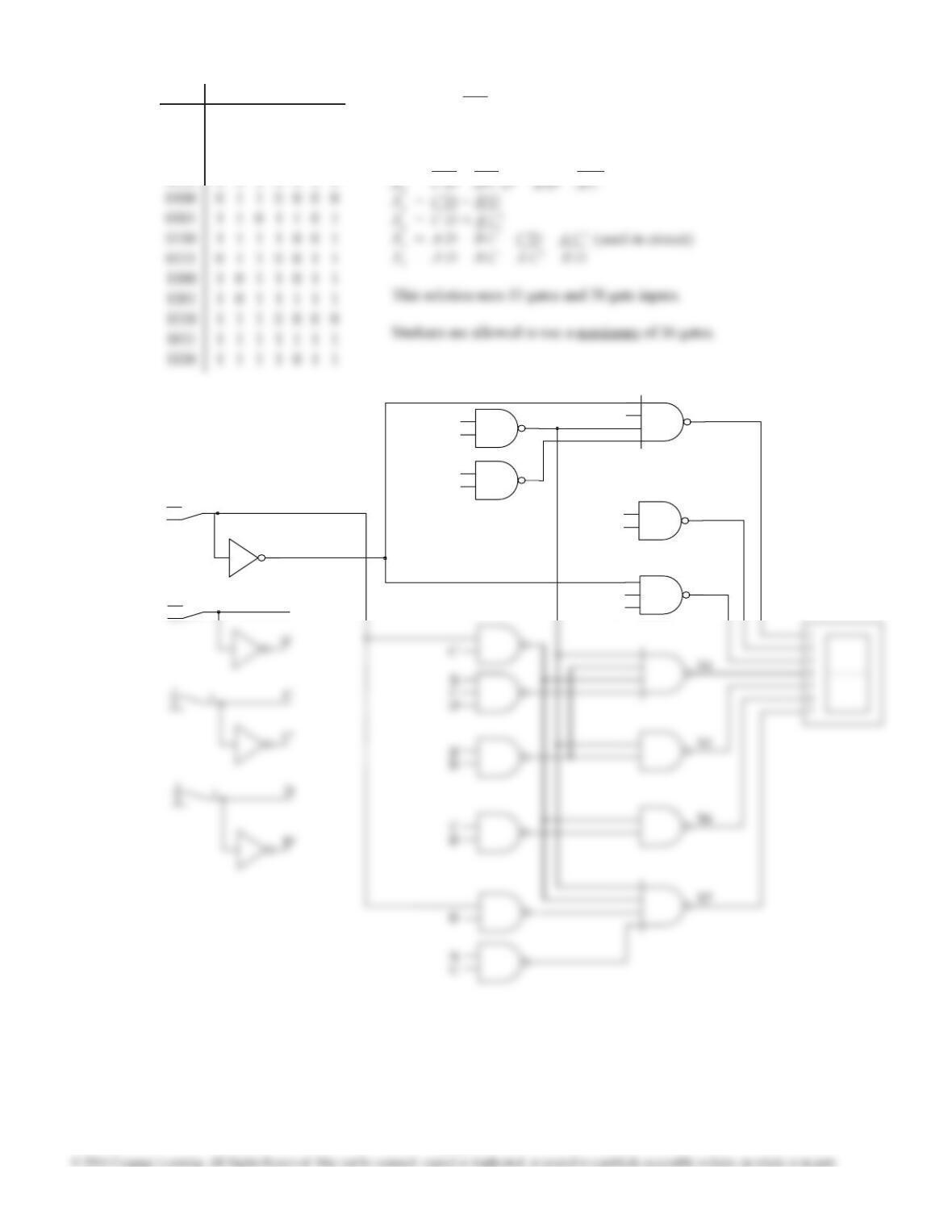
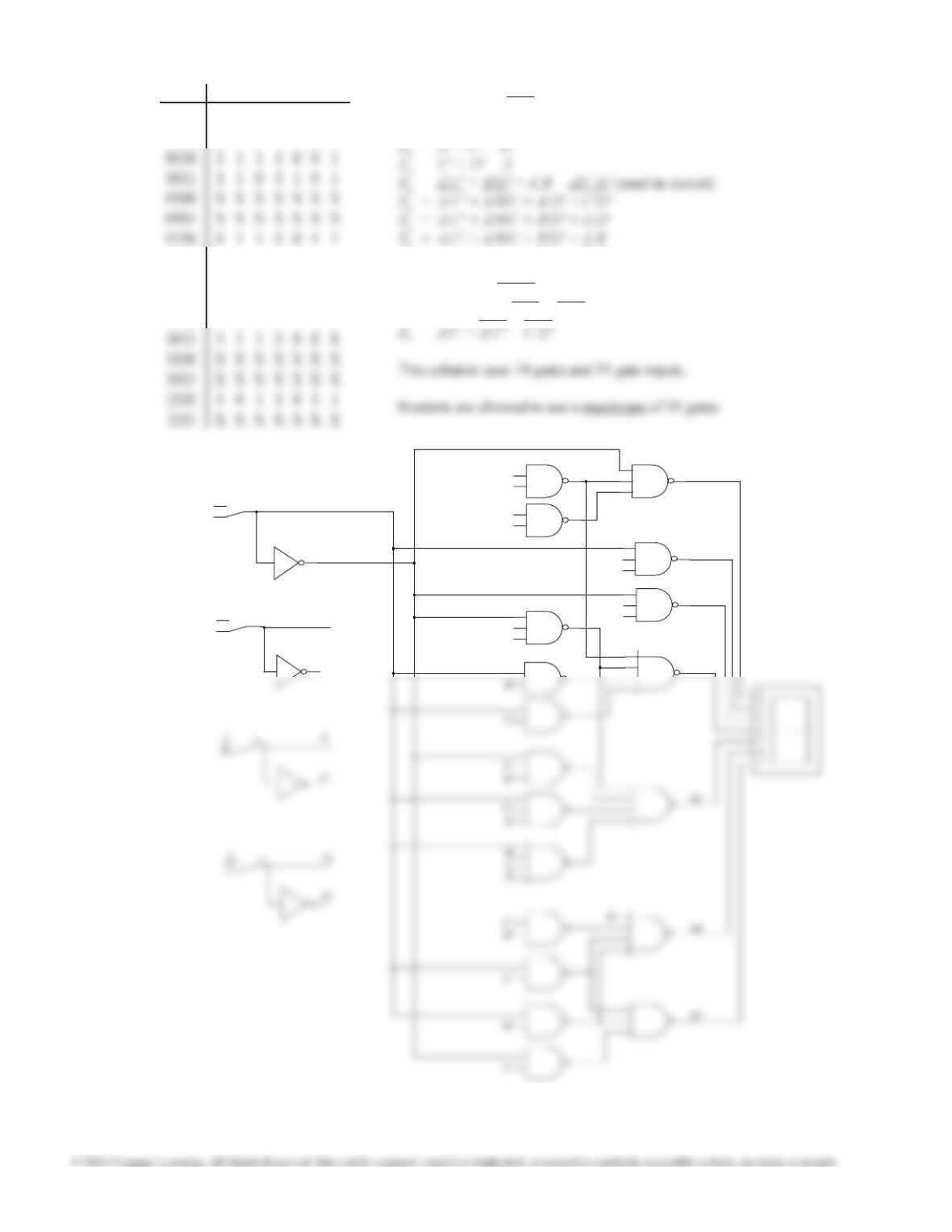
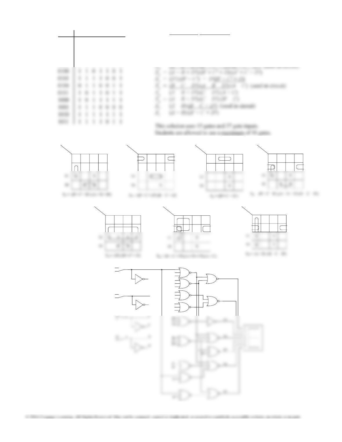
8.C W = A(C + D) (B + C) (C + E) = A(C + BDE) (used in circuit)
W = A(C + D) (B + C) (D’ + E)
W = A(C + D) (C + E) (B + D’)
W = A(C + D) (B + D’) (D’ + E)
X = (C + D) (B’ + C + E’) (A + C) (B + C’) =
Z = B E
This solution uses 14 gates and 32 gate inputs.
Student are allowed to use a maximum of 15 gates.
00000 0 0 0 0
00001 0 0 0 0
00010 0 0 0 0
00011 0 0 0 0
01101 0 1 0 1
01110 X X X X
01111 X X X X
10000 0 0 0 0
10001 0 0 1 0
10010 0 1 0 0
10011 0 1 1 0
10100 1 0 0 0
ABCDE W X Y Z
Unit 8 Design Solutions
267
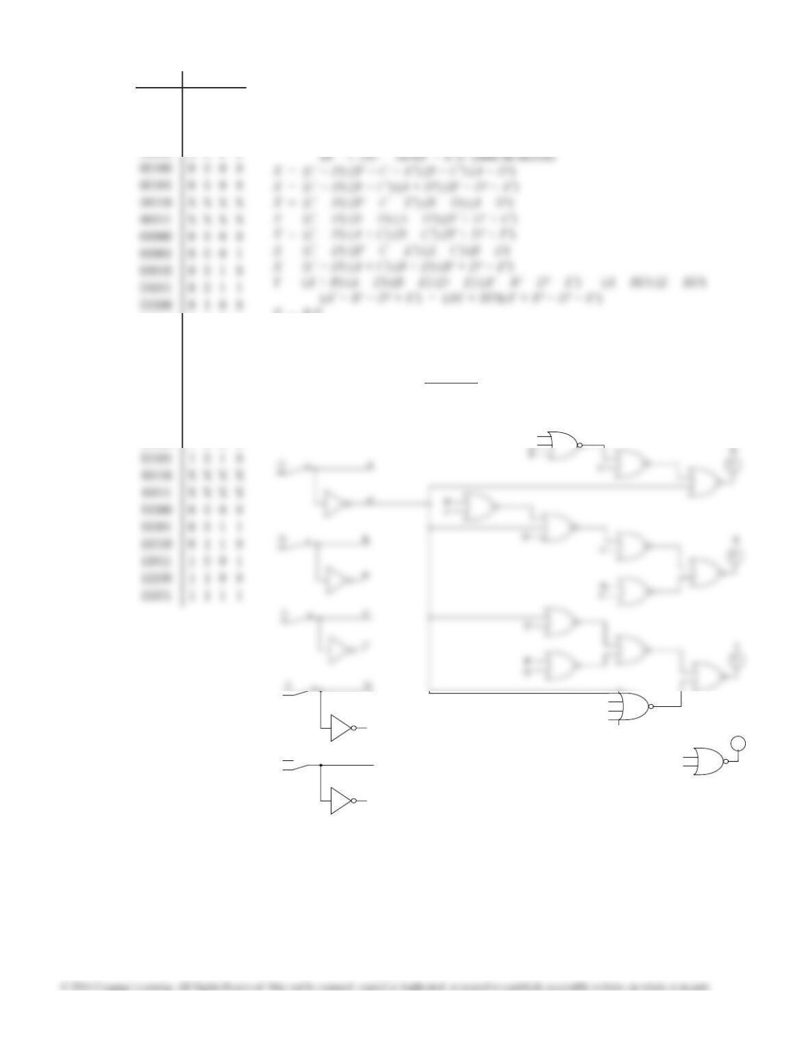
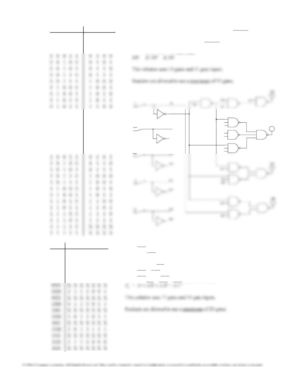
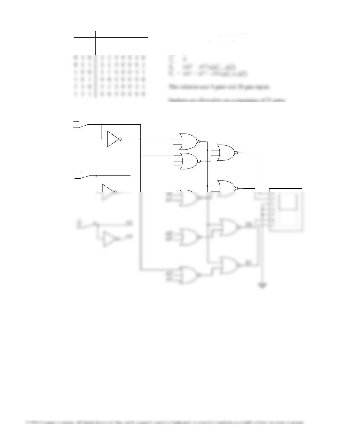
8.D W = A C + A B D E
X = B C + A B’D + A D E’
Y = A’B D + A B’E + A D’E + B D E’
Z = B E
This solution uses 14 gates and 38 gate inputs.
Students are allowed to use a maximum of 14 gates.
Y
B C
D E
00 01 11 10
00
1
1
1
1
Z
B C
D E
00 01 11 10
00
1
1
00000 0 0 0 0
00001 0 0 0 0
00010 0 0 0 0
00011 0 0 0 0
10000 0 0 0 0
10001 0 0 1 0
10010 0 1 0 0
10011 0 1 1 0
ABCDE W X Y Z
X
B
D
E
B’
D
D
B
C
1
00
1
00
B
B’
C
0
Unit 8 Design Solutions
268
8.E X1 = A B + A’C + B’D +
C’D’ (used in circuit)
X1 = A C’ + B C + B’D + A’D’
A’B’ (used in circuit)
X3 = A B + B’C + A’D + C’D’
C’D’ (used in circuit)
X4 = X1
X5 = B’D + B D’ + C’D’ +
A’B’ (used in circuit)
X5 = B’D + B D’ + C’D’ + A’D’
X5 = B’D + B D’ + A’D’ + B’C’
X5 = B’D + B D’ + A’B’ + B’C’
X6 = A’B’ + C’D’ + A C
18 gates.
1
2
CX2
X3
C
B’
D’
B
D
B’
1
00
1
00
B
B’
C
0000 1 1 1 1 1 1 0
0001 1 1 1 1 1 1 0
0111 1 1 1 1 0 0 1
1000 1 1 1 1 1 1 0
1001 1 1 0 1 1 0 1
1111 1 1 1 1 0 1 1
ABCD X
1
X
2
X
3
X
4
X
5
X
6
X
7
Unit 8 Design Solutions
269
8.F X1 = A + B’C + B’D’ (used in circuit)
X1 = A + B’C + C’D’
X1 = A + B’D’ + C D
X4 = A C’ + B’D’ + A D’ + A’C D
X5 = A’C’D’ + A’C D + A C’D + A B’C D’
X6 = C’D’ + B + A C’ + A D’
X7 = A’C + A C’ + A D’ (used in circuit)
0000 1 1 1 1 1 1 0
0001 0 1 1 0 0 0 0
0111 X X X X X X X
1000 1 1 1 1 0 1 1
1001 1 1 1 1 1 1 1
1010 1 0 1 1 1 1 1
ABCD X
1
X
2
X
3
X
4
X
5
X
6
X
7
X1
C
D’
X2
C
D
X3
B’
D’
B’
C
C
D
X4
1
00
1
00
A
A’
B
B’
Unit 8 Design Solutions
270
8.G
M2
N2′
N1
N2
N1′
N2
N0′
1
00
1
K’
N3
N3′
0
8.H X1 = A’C’ + D + B + A C
X2 = A’ + B’C’ + B C
X3 = B’ + C + A
X4 = X5 + D + A’B + A B’C
X5 = A’C’ + B C’
X6 = B’C’ + D + A B’ + A C’
X7 = D + A’B + A B’ + B C’ (used in circuit)
0000 1 1 1 1 1 1 0
0001 1 1 1 1 1 1 1
0010 0 1 1 0 0 0 0
0011 1 1 1 1 0 1 1
0100 1 1 0 1 1 0 1
ABCD X
1
X
2
X
3
X
4
X
5
X
6
X
7
M3 = N2 N1 N0 + N3 + K N2 N1 = N3 + N2 N1(K + N0)
M2 = N2 N1′ + K’N2 N0′ + N2’N1 N0 + K N2′ N1
= N2 N1′ + K’ N2 N0′ + N2′ N1(K + N0)
M1 = K’N1 N0′ + K N1′ + N1’N0
= K’ N1 N0′ + N1′(K + N0)
0 0 0 0 0 0 0 0 1
0 0 0 0 1 0 0 1 0
0 0 0 1 0 0 0 1 1
0 1 1 0 0 1 1 0 1
0 1 1 0 1 1 1 1 0
0 1 1 1 0 1 1 1 1
0 1 1 1 1 X X X X
1 0 0 0 0 0 0 1 0
1 0 0 0 1 0 0 1 1
1 0 0 1 0 0 1 0 0
K N3 N2 N1 N0 M3 M2 M1 M0
Unit 8 Design Solutions
271
B’
D’
X1
X2
B
C’
X3
D’
C’
C
B’
C’
B
C
1
00
1
00
A
A’
B
B’
8.H
(cont.)
8.I
X1 = B’D’ + C’ + B D + A
X2 = B’C + C’D + B D’ (used in circuit)
X2 = B’C + A’D’ + C’D
X2 = B’D + C D’ + B C’
X2 = B’D + A’C’ + C D’
X3 = D + C + B’ (used in circuit)
0000 X X X X X X X
0001 X X X X X X X
0010 1 1 1 1 1 1 0
0011 0 1 1 0 0 0 0
ABCD X
1
X
2
X
3
X
4
X
5
X
6
X
7
CX1
X6
B’
X7
B’
D’
B
D
B’
C
D’
B
C
C
1
00
1
00
A
A’
B
Unit 8 Design Solutions
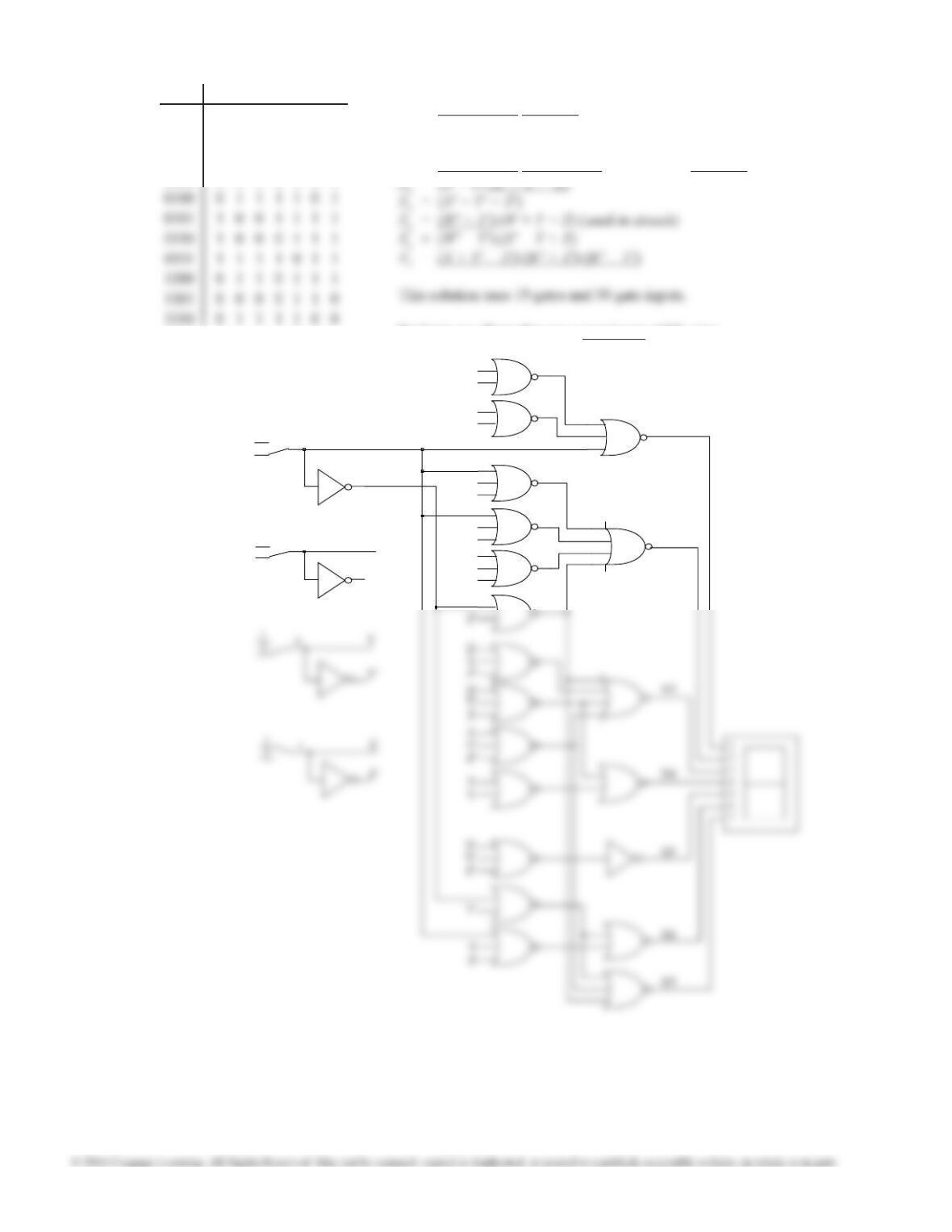
8.J W = (A + B + C) (C + D) (B’ + C + E) (used in circuit)
W = (A + B + C) (C + D) (A + C + E)
Z = (A + B) (C + E) (A + D + E) (used in circuit)
Z = (A + B) (C + E) (B’ + D + E)
This solution uses 17 gates and 51 gate inputs.
Y
Z
B’
C
E
C
E’
B’
C
D’
E’
C
D
B
E
D
E
B
C
E
00
1
00
A’
D
D’
E
E’
0
0
00110 1 1 0 0
00111 1 1 1 0
01000 0 0 0 0
01111 1 1 1 1
10000 0 0 0 0
10001 0 1 0 1
10010 1 0 1 0
ABCDE W X Y Z
Unit 8 Design Solutions
273
8.K W = A B
X = B C + A B’
Y = B’C D + A’B C’ + A B’D + A C
W
Y
C
B
C’
B’
D
B’
C
1
00
B’
C
C’
0
0
00000 0 0 0 0
01000 0 0 1 0
01001 0 0 1 1
01010 0 0 1 1
01011 0 0 1 1
10010 0 1 1 0
10011 0 1 1 0
10100 0 1 1 0
10101 0 1 1 1
10110 0 1 1 1
ABCDE W X Y Z
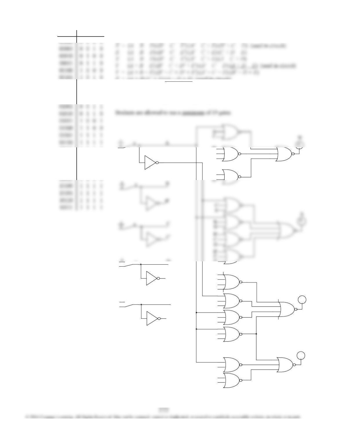
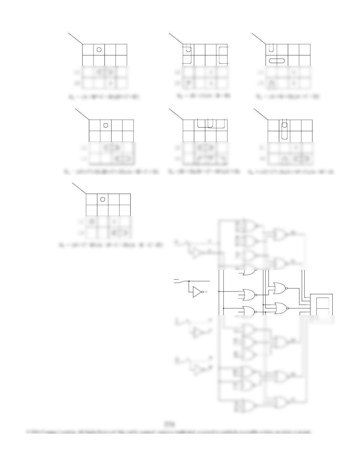
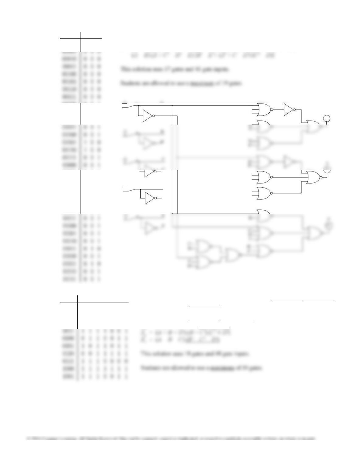
8.L X1 = (A + B’ + C + D) (B’ + C’ + D’)
X2 = (B + C) (A + B + D)
X3 = (A + B + D) (A + C + D’)
X4 = (A + B’ + C + D) (B’ + C’ + D’) (A’ + C’ + D)
X5 = (B’ + D) (B’ + C’) (A’ + D) = (B’ + D) (B’ + C’ + D’) (A’ + D)
X6 = (A’ + C’ + D) (A + B’ + D) (A + B’ + C) (used in circuit)
X6 = (A’ + C’ + D) (A + B’ + C) (B’ + C’ + D)
0000 1 0 0 1 1 1 1
0001 1 0 0 1 1 1 1
0010 1 0 0 1 1 1 1
0011 1 1 1 1 1 1 0
0100 0 1 1 0 0 0 0
ABCD X
1
X
2
X
3
X
4
X
5
X
6
X
7
Unit 8 Design Solutions
A B
C D 00 01 11 10
00
01
0
X
A B
C D 00 01 11 10
00
01
0
0
0
0X
A B
C D 00 01 11 10
00
01
0
0
0 X
A B
C D 00 01 11 10
00
01
0
X
A B
C D 00 01 11 10
00
01
0
0
0
X
A B
C D 00 01 11 10
00
01
0
0
X
A B
C D 00 01 11 10
00
01
0
X
8.L
(cont.)
1
2
3
4
5
X3
X4
B
D
C
D’
C’
1
00
B
B’
Unit 8 Design Solutions
275
8.M X1 = W’(X + Z) (Y + Z)
X2 = (X’ + Y + Z’) (W’ + Z’) (W + Y’ + Z ) (W + X + Y’) (used in circuit)
X2 = (X’ + Y + Z’) (W’ + Z’) (W + X + Y’) (X’ + Y’ + Z)
X2 = (X’ + Y + Z’) (W’ + Z’) (W + Y’ + Z) (X + Y’ + Z’)
X3 = (X + Y’ + Z’) (X’ + Y + Z’) (X’ + Y’ + Z) (W’ + Z’)
Students are allowed to use a maximum of 22 gates.
0000 X X X X X X X
0001 1 1 1 0 1 1 1
0010 0 0 1 1 1 1 1
0011 1 0 0 1 1 1 0
WXYZ X
1
X
2
X
3
X
4
X
5
X
6
X
7
X1
X2
X
Z
Y
Z
X
Y’
Y’
Z
X’
Y
Z’
1
00
1
00
W
W’
X
X’
Unit 8 Design Solutions
276
X
B’
C’
C
D
C’
D’
00
1
00
A
A’
C’
D
D’
0
8.O X1 = (A + B + C + D’) (B’ + D) = (A + B + C + D’) (B’ + C’ + D) (B’ + C + D)
X2 = (B’ + C + D’) (B’ + C’ + D)
X3 = (B + C’ + D)
X4 = (B + C + D’) (B’ + C + D) (B’ + C’ + D’)
X5 = D’ (B’ + C) = D’ (B’ + C + D)
0000 1 1 1 1 1 1 0
0001 0 1 1 0 0 0 0
0010 1 1 0 1 1 0 1
ABCD X
1
X
2
X
3
X
4
X
5
X
6
X
7
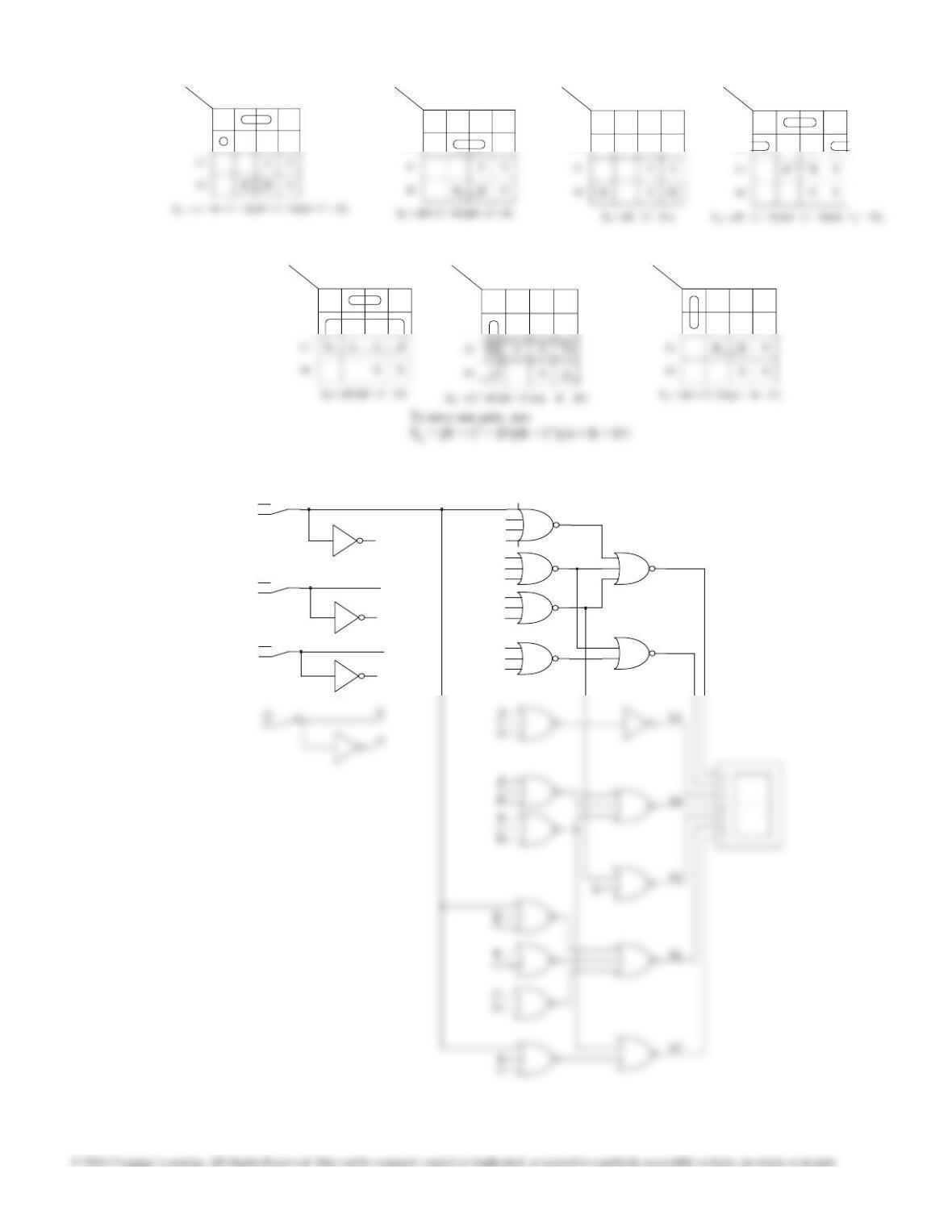
8.N X = A’BC(D + E) (D’ + E’)
Y = ABE(C + D) (C’ + D’)
Z = (A + B) (A + C’ + D’ + E) (A’ + B’ + C + D’ + E’) (B’ + C’ + D + E’)
00000 0 0 0
01000 0 0 1
01001 0 0 1
01010 0 0 1
10001 0 0 1
10010 0 0 1
10011 0 0 1
10100 0 0 1
10101 0 0 1
10110 0 0 1
ABCDE X Y Z
Unit 8 Design Solutions
277
A B
C D 00 01 11 10
00
01
0
0
X
X
A B
C D 00 01 11 10
00
01
0
X
X
A B
C D 00 01 11 10
00
01
X
X
A B
C D 00 01 11 10
00
01
0
0
0
X
X
A B
C D 00 01 11 10
00
01
0
0
0
0
X
X
A B
C D 00 01 11 10
00
01
0
0
X
X
A B
C D 00 01 11 10
00
01
0
X
X
8.O
(cont.)
X1
X2
B
C
D’
B’
C’
D
B’
C
D
B’
C
D’
1
00
1
00
1
00
A
A’
B
B’
C
C’
Unit 8 Design Solutions
278
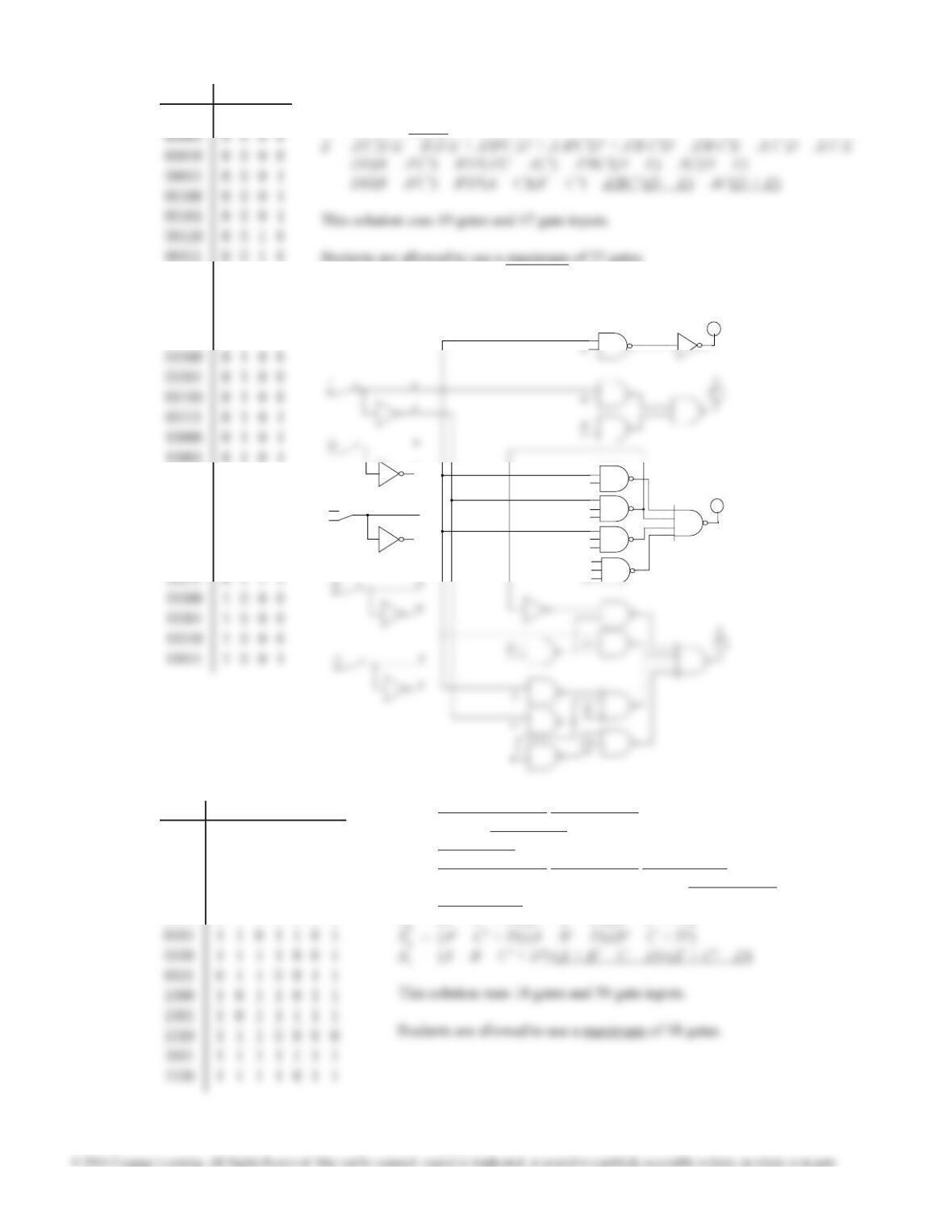
8.P X1 = (A + C + D’) (A + B’)
X2 = (A’ + C’ + D)
X3 = (A + C’ + D’)
Students are allowed to use a maximum of 21 gates.
3
4
5
6
7
X4
B
X5
B’
C’
D’
C
C’
D
C
D’
1
00
1
00
A
A’
D
D’
0000 1 1 1 1 1 1 0
1000 1 1 1 1 0 1 1
1001 1 1 1 1 1 1 1
1010 1 0 1 1 1 1 1
1011 1 1 1 0 0 0 0
ABCD X
1
X
2
X
3
X
4
X
5
X
6
X
7
8.Q X1 = (A + B + C’ + D) (A’ + B + C)
X2 = (A’ + B + C’) (A’ + B’ + C)
X3 = (A + B’ + C)
X4 = (A + B + C’ + D) (A’ + B + C) (A’ + B’ + C’)
X5 = C’(A’ + B) = C’(A’ + B + C)
X6 = (A + C’ + D) (A + B’ + C) (A’ + B’ + C’)
0000 1 1 1 1 1 1 0
0001 1 1 1 1 1 1 1
0010 0 1 1 0 0 0 0
0011 1 1 1 1 0 1 1
ABCD X
1
X
2
X
3
X
4
X
5
X
6
X
7
Unit 8 Design Solutions
279
X
A B
C D 00 01 11 10
00
01
X
0
X
X
1X
A B
C D 00 01 11 10
00
01
X
X
0
X
2X
A B
C D 00 01 11 10
00
01
0
X
X
X
3X
A B
C D 00 01 11 10
00
01
X
0
X
X
4
X
A B
C D 00 01 11 10
00
01
X
0
X
X
5
A B
C D 00 01 11 10
00
01
0
X
X
X
X
A B
C D 00 01 11 10
00
01
0
X
X
X
7
8.Q
(cont.)
X1
X2
B
C
B
C’
D
B
C’
B’
C
1
00
1
00
1
00
A
A’
B
B’
C
C’
Unit 8 Design Solutions
280
X1
X2
B
D’
B’
C’
D
B’
C’
D’
B
C
D
1
00A
A’
1
00
B
B’
A B
C D 00 01 11 10
00
01
X
X
X
X
A B
C D 00 01 11 10
00
01
X
X
0X
X
A B
C D 00 01 11 10
00
01
X
X
0 X
X
A B
C D 00 01 11 10
00
01
X
X
0
X
X
A B
C D 00 01 11 10
00
01
X
X
0
0
X
X
A B
C D 00 01 11 10
00
01
X
X
0
0 0
X
X
A B
C D 00 01 11 10
00
01
X
X
0
X
X
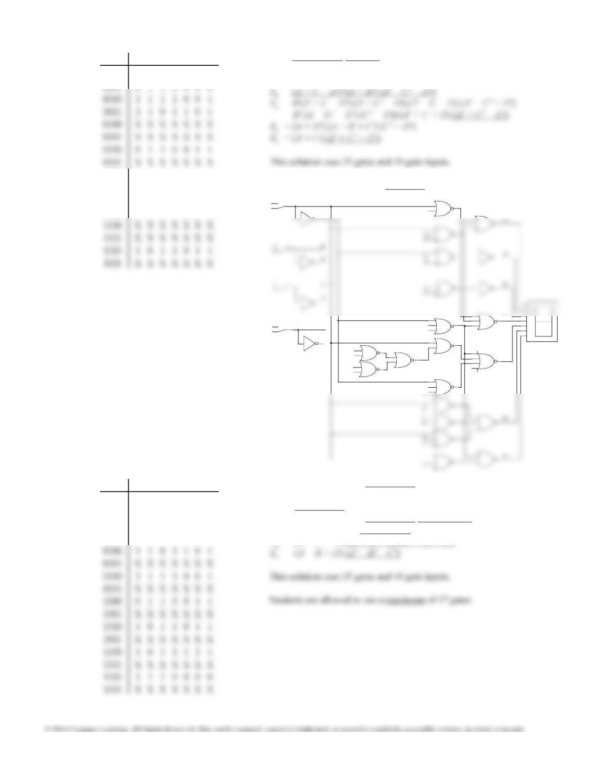
8.R X1 = (A + B + D’) (B’ + C’ + D)
X2 = (B’ + C’ + D’) (B + C + D) (used in circuit)
X2 = (B’ + C’ + D’) (A’ + C + D)
X3 = (B’ + C + D) (used in circuit)
X3 = (A + C + D)
0000 X X X X X X X
0001 X X X X X X X
0010 1 1 1 1 1 1 0
0011 0 1 1 0 0 0 0
ABCD X
1
X
2
X
3
X
4
X
5
X
6
X
7
Unit 8 Design Solutions
281
X1
X2
A3′
A2
A3
1
00A1
A1′
1
00
A2
A2′
8.S X1 = (A1 + A2 + A3) (A1′ + A3′)
X2 = (A2 + A3′) (A1′ + A3′)
X3 = 0
X4 = 0
0 0 0 0 1 0 0 0 1 1
0 0 1 1 0 0 0 0 1 1
A1 A2 A3 X
1
X
2
X
3
X
4
X
5
X
6
X
7

Unit 8 Design Solutions
282