22
1. Draw the entire schematic with .020 in. (0.5 mm) wide lines
and dashed stage lines .028 in. (0.7 mm) wide.
2. Do all lettering .12 in. (3 mm) high with titles .24 in. (6mm) high.
3. Reference designators are not shown; use the left-to-right
and top-to-bottom labeling system, using coding as de-
scribed in this chapter: R1, R2, R3 . . . , C1, C2. . . .
4. Label horizontal components above and vertical compo-
nents to the right.
5. Place connection dots as necessary.
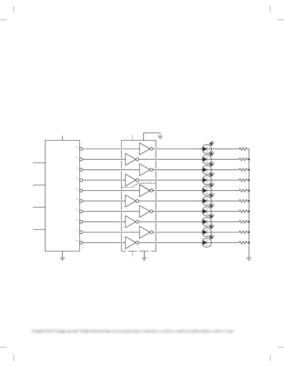
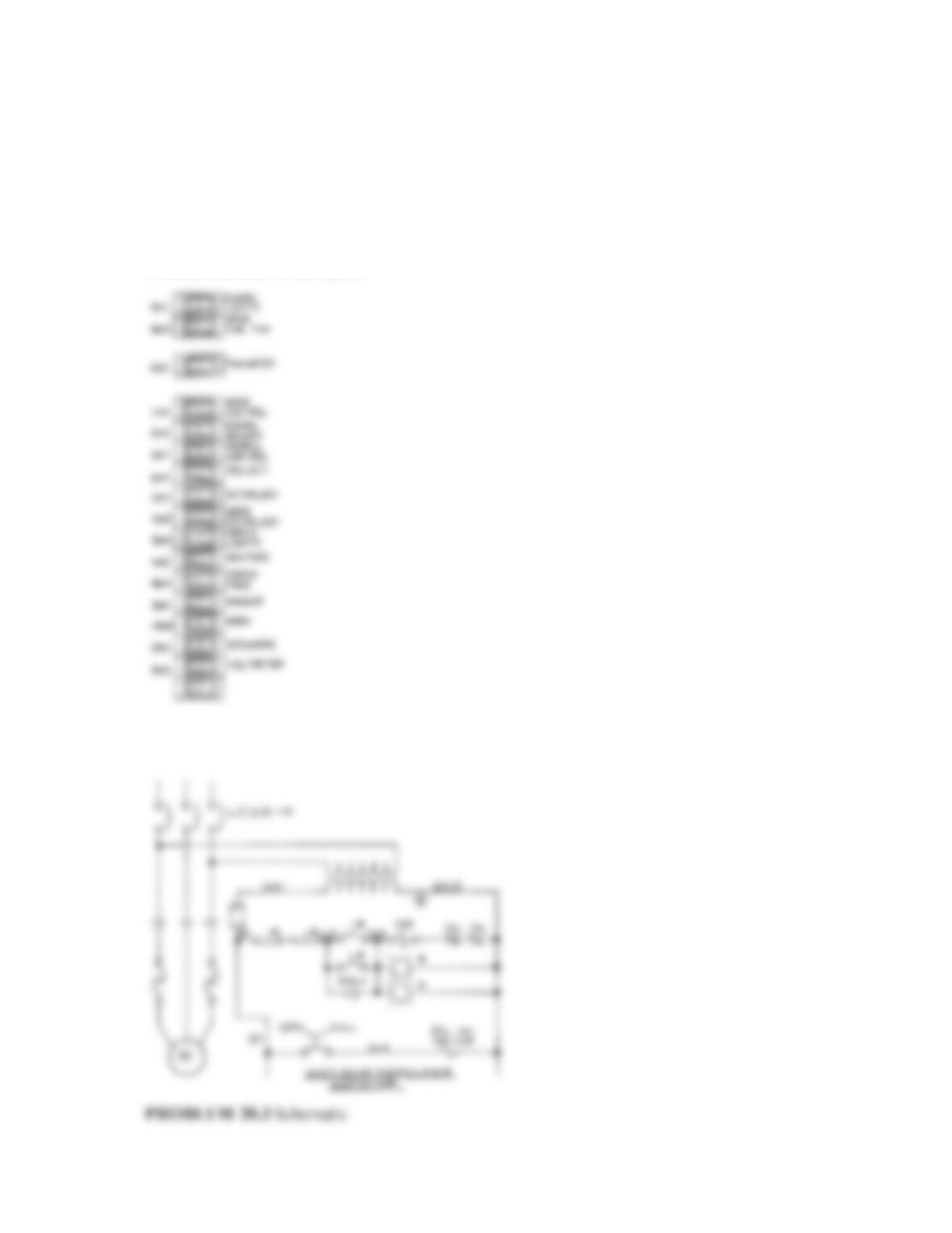
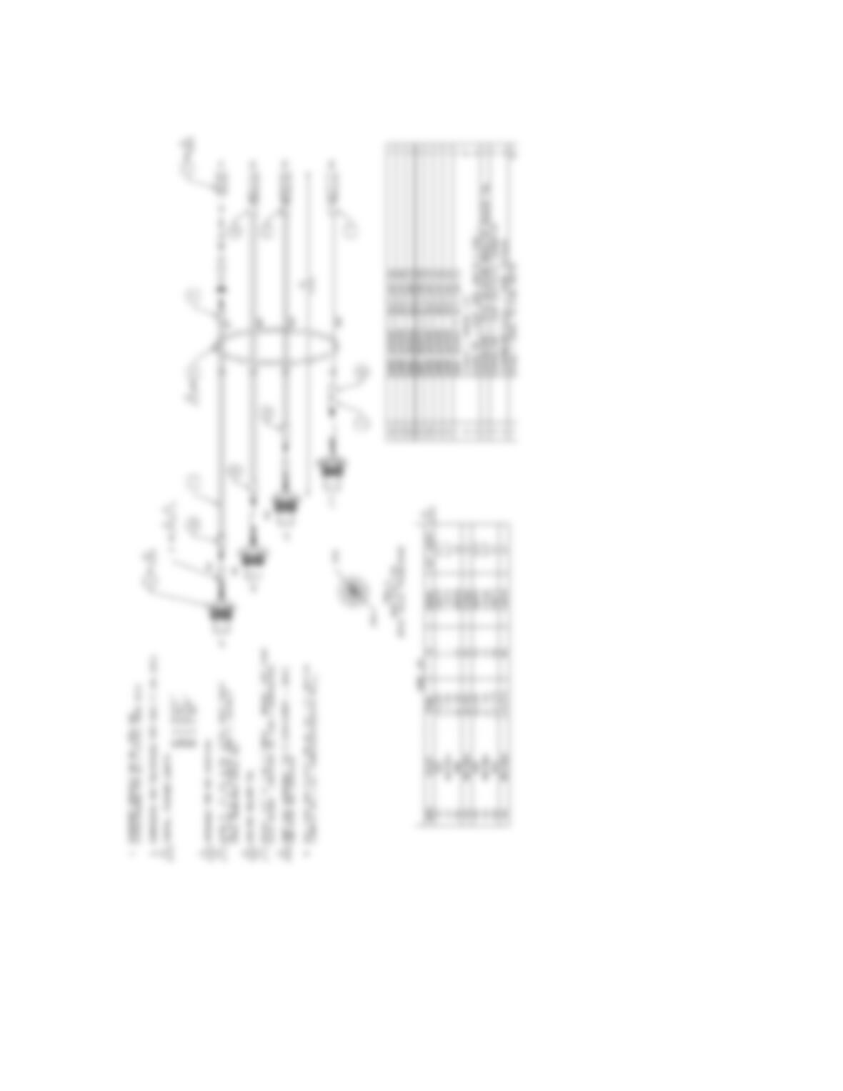
PROBLEM 20.45 Schematic diagram
Given the schematic engineering sketch, make a schematic dia-
gram using 17 3 22 (A2 metric) size. There is no scale, and the
drawing must be balanced, uncluttered, and easy to read. Use the
following instructions unless otherwise specified by your
instructor:
1. Draw the entire schematic with .020 in. (0.5 mm) wide lines
and dashed stage lines .028 in. (0.7 mm) wide.
2. Do all lettering .12 in. (3 mm) high with titles .24 in. (6mm) high.
3. Reference designators are not shown; use the left-to-right
and top-to-bottom labeling system, using coding as de-
scribed in this chapter: R1, R2, R3 . . . , C1, C2. . . .
4. Label horizontal components above and vertical compo-
nents to the right.
5. Place connection dots as necessary.
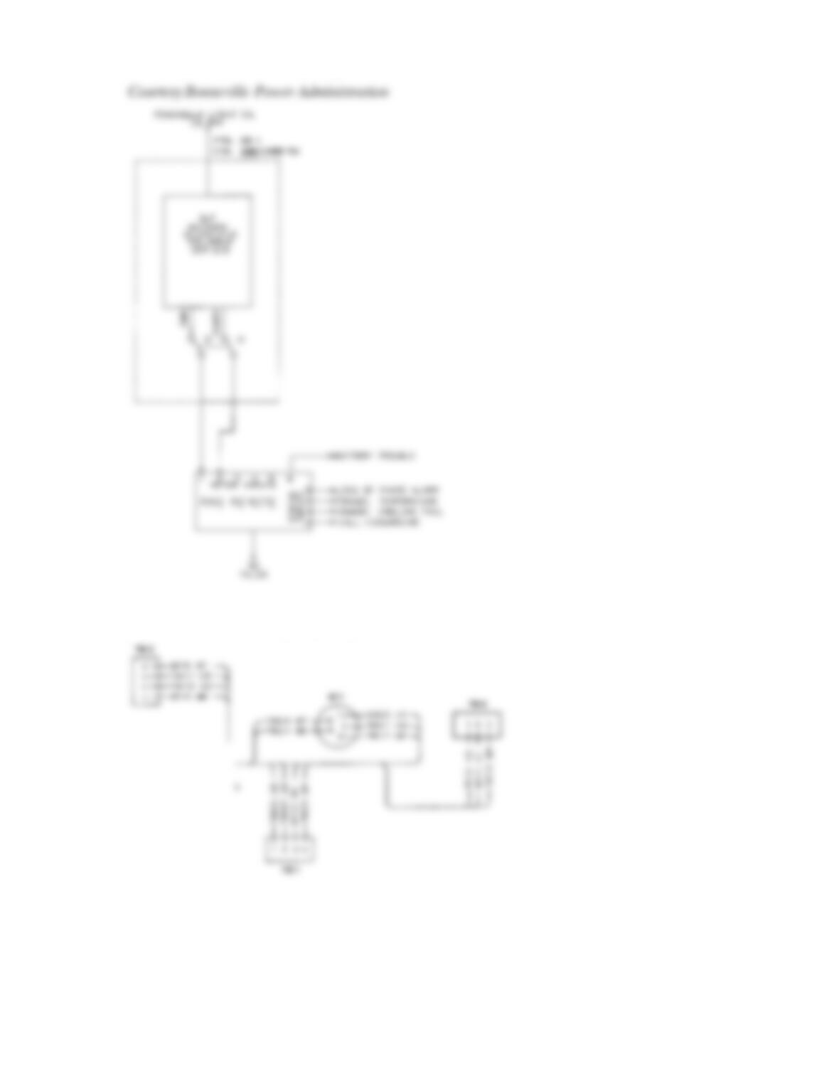
Courtesy RCA Consumer Electronics
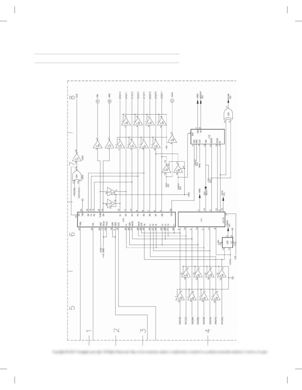
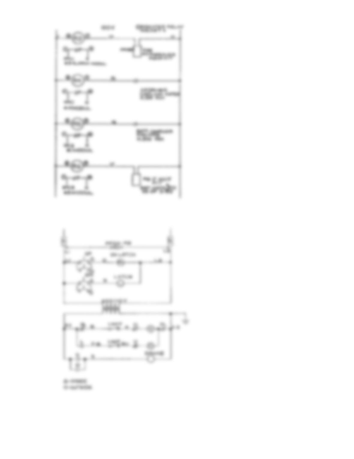
0
7
14
15V
14 7
15V
15V
8
6
10
12
8
6
10
4
12
2
1
16
Vcc
DECODER
(7442)
U1
GND
2
3
4
5
6
7
A
B
1s
2s
4s
8s
C
D
15
14
13
BINARY
INPUT
12
9
10
11
1. REFERENCE DESIGNATORS ARE FOR REFERENCE ONLY AND MAY NOT APPEAR ON PART.
2. RESISTOR VALUES ARE IN DHMS.
3. FOR PWB/COMPONENT ASSEMBLY, SEE DWG. 100/01.
4. FOR PARTS, SEE SPL 100/02.
5. FOR PRINTED WIRING BOARD, SEE DWG. 100/03.
0
1
2
3
4
5
6
7
8
9
8
9
U3
7404
5
11
13
9
5
11
3
13
1
1
2
3
4
5
6
7
8
9
R1
DECIBAL OUTPUT
150
R2
150
R3
150
R4
150
R5
150
R6
150
R7
150
R8
150
R9
150
R10
DR 10
XC556R
DR 9
XC556R
DR 8
XC556R
DR 7
XC556R
DR 6
XC556R
DR 5
XC556R
DR 4
XC556R
DR 3
XC556R
DR 2
XC556R
DR 1
XC556R
150
U2
7404
NOTES:
59728_ch20_EOC_ptg01.indd 22 22/02/16 10:50 am
23
ADVANCED PROBLEMS
Part 5: Problems 20.46 Through 20.52
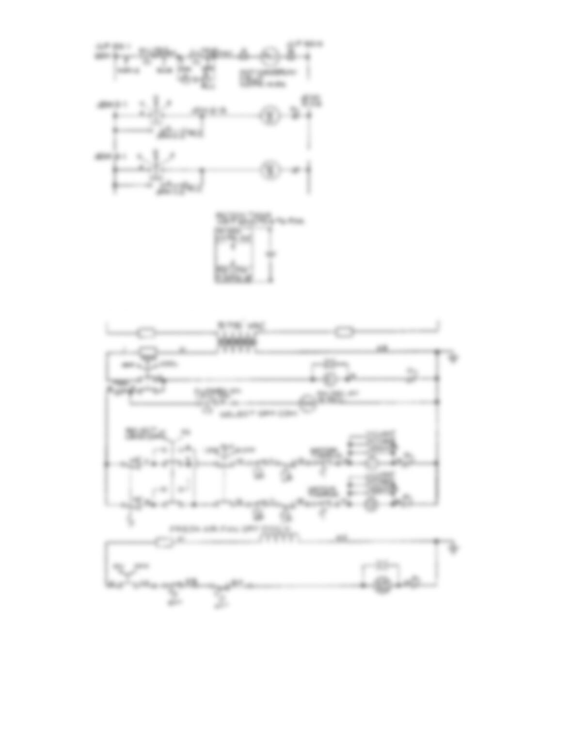
PROBLEM 20.46 Schematic diagram
59728_ch20_EOC_ptg01.indd 23 22/02/16 10:50 am
24
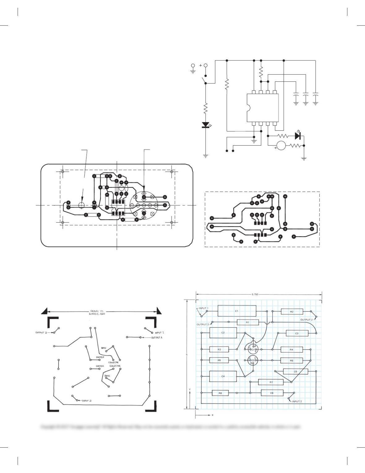
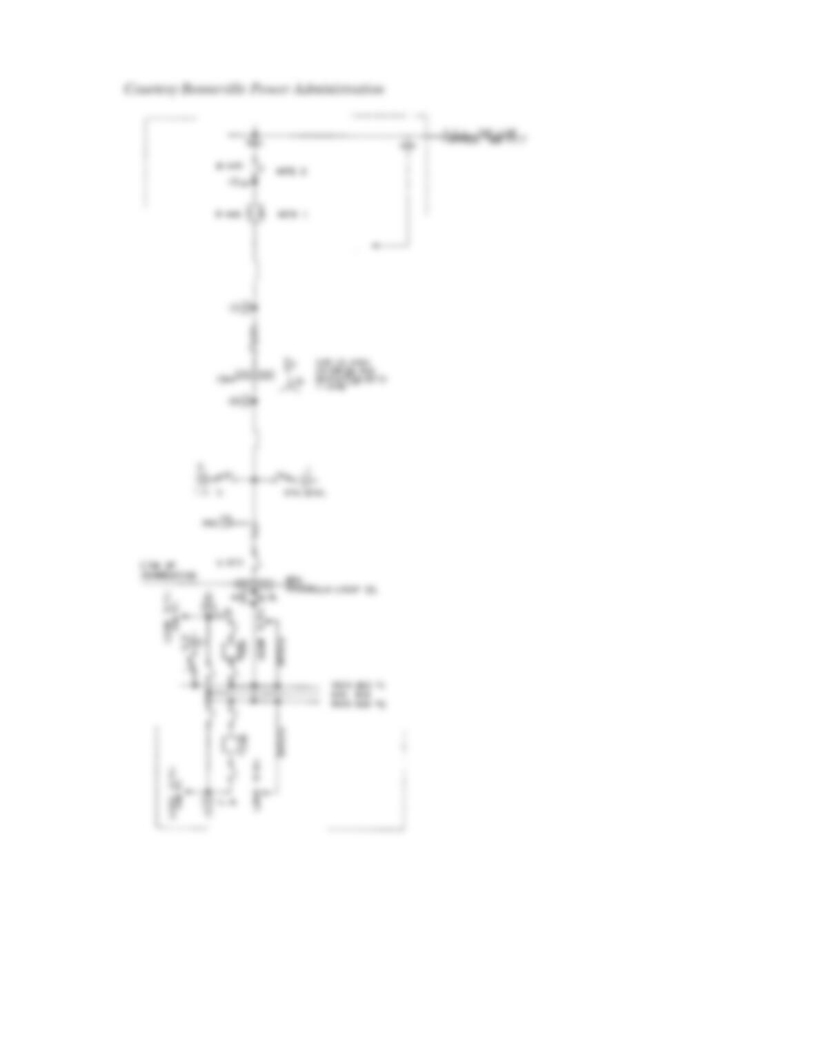
PROBLEM 20.47 Continuity tester
Given a schematic layout, create a schematic drawing, silk screen
artwork, drilling drawing, and circuit side and component side
board. Use 5/320 (4 mm) high lettering. All through hole compo-
nents have AWB 24 size. There are four #35 mount holes that are
.125 in. (3 mm) from each side at each corner. The finished size
of the board is 1-1/20 3 2-1/160 (33 3 52 mm) dimensions.
Reprinted from TECH DIRECTIONS, April 1999, Ann Arbor,
MI. Courtesy Harry M. Hawkins, Professor Emeritus, Oswego State
University of New York.
9V
10k
47 pF 10 uF
1k
555
1234
6758
PROBE
22 ohm
47k
1k
LED
(GREEN)
LED
(RED)
ELECTRONIC
BUZZER
ON/OFF
0.1 uF
CONTINUITY TESTER
(a)
_
+
.1uF
1k
10k
47 pF
10uF
RED GREEN
1k
555
+
22 ohm
+
47k
9V
ELECTRONIC
BUZZER
PROBES
CONTINUITY
Ø3/16 DRILL #35 (15 HOLES)
COMPONENT SIDE
(
b
)(
c
)
FOIL SIDE
TESTER
PROBLEM 20.48 Printed circuit board layout
Given the “component side” engineer’s sketch of a printed circuit
board, make a printed circuit board layout on the “back side” at
2:1 scale. Use the following instructions unless otherwise speci-
fied by your instructor:
1. Use PCB graphics or CADD software.
2. Use teardrop pads with fi llet radius, .2000 (5 mm) OD and
.0320 (0.8 mm) ID.
3. Use .0800 (2 mm) trace line width.
59728_ch20_EOC_ptg01.indd 24 22/02/16 10:50 am
25
PROBLEM 20.49 Silk screen artwork
Given the PCB layout sketch from Problem 20.48, make a silk
screen artwork at 1:1 scale. Use 5/320 (4 mm) high lettering with
ink and mechanical lettering device or rub-on letters, unless
otherwise specified by your instructor.
PROBLEM 20.50 Drilling drawing
Given the PCB layout from Problem 20.48 and the dimension
table shown here, prepare a drilling drawing using tabular di-
mensioning. Refer to Chapter 10, Dimensioning and Tolerancing.
The holes may be shown using centerline “cross” at the center
locations without drawing the actual circles. The 0,0 location is
at the lower left corner of the PCB. Number the holes from top to
bottom and left to right as coordinated with the given table.
NOTE: Dimensions are given from component
side.
Hole No. X Y Diameter
1 .500 4.500 .032
2 3.250 4.500 .032
3 3.500 4.500 .032
4 5.250 4.500 .032
5 5.500 4.250 .032
6 .750 4.000 .032
7 1.500 4.000 .032
8 3.500 4.000 .032
9 .250 3.500 .032
10 2.250 3.500 .032
11 3.750 3.500 .032
12 5.500 3.500 .032
13 2.625 3.250 .032
14 .250 2.750 .032
15 1.875 2.750 .032
16 2.250 2.750 .032
17 3.000 2.750 .032
18 3.500 2.750 .032
19 5.250 2.750 .032
20 .250 2.250 .032
21 1.875 2.250 .032
22 2.250 2.250 .032
23 3.000 2.250 .032
24 3.500 2.250 .032
25 5.250 2.250 .032
26 2.625 1.750 .032
27 3.625 1.750 .032
28 5.500 1.750 .032
29 .250 1.500 .032
30 2.250 1.500 .032
31 2.500 1.250 .032
32 4.375 1.250 .032
33 .250 .750 .032
34 1.875 .750 .032
35 2.500 .750 .032
36 4.500 .750 .032
37 4.250 .500 .032
Pictorial Drawing
Given the engineer’s layout, make a pictorial drawing using any
one of the specific shading techniques discussed in Chapter 14,
Pictorial Drawings and Technical Illustrations. Scale the engi-
neer’s layout directly to determine dimensions. Increase the size
of your final drawing. Place all labels on the final drawing in ink
using mechanical lettering devices, or prepare a CADD plot if
available.
PROBLEM 20.51 Exploded technical illustration
Given the exploded technical illustration shown in Figure 20.90
on page 709, select and draw the pictorial of any one subassem-
bly unless otherwise specified by your instructor. Make your
drawing larger but proportional to the given drawing.
PROBLEM 20.52 Pictorial schematic
Given the semipictorial schematic engineering layout shown in
Figure 20.91 on page 710, make a formal drawing.
ENVIRONMENTAL REPORT
Part 6: Problem 20.53
PROBLEM 20.53 Write and give a 250 word oral report with
graphics covering electrical generation from wind power.
MATH PROBLEMS
Part 7: Problems 20.54 Through 20.63
Convert these numbers to power of ten form:
PROBLEM 20.54 243
PROBLEM 20.55 14,000
PROBLEM 20.56 .004
59728_ch20_EOC_ptg01.indd 25 22/02/16 10:50 am

26
Convert these numbers to regular form:
PROBLEM 20.57 6.7 3 103
PROBLEM 20.58 9 3 106
PROBLEM 20.59 6.2 3 1023
Perform these calculations:
PROBLEM 20.60 (4 3 106) (3 3 1013)
PROBLEM 20.61 25 3 1017/5 3 1011
PROBLEM 20.62 (7 3 1026) (5 3 1022)
PROBLEM 20.63 2.8 3102
6
8.
131
0
5
59728_ch20_EOC_ptg01.indd 26 22/02/16 10:50 am
350
Chapter 20
Electrical and Electronic Drafting
Solutions to End-of-Chapter Problems
Part 1: Problems 20.1 Through 20.10
PROBLEM 20.1 Switch panel
PROBLEM 20.2 Schematic
351
PROBLEM 20.4 Schematic
PROBLEM 20.5 Schematic
352
PROBLEM 20.6 Schema tic
353
PROBLEM 20.7 Block diagram
354
PROBLEM 20.8 Elementary diagram
PROBLEM 20.9 Highway diagram
355
PROBLEM 20.10 Wireless diagram
356
Part 2: Problems 20.11 Through 20.15
PROBLEM 20.11 Cable diagram
357
PROBLEM 20.12 Wiring diagram
358
PROBLEM 20.13 Wireless diagram
359
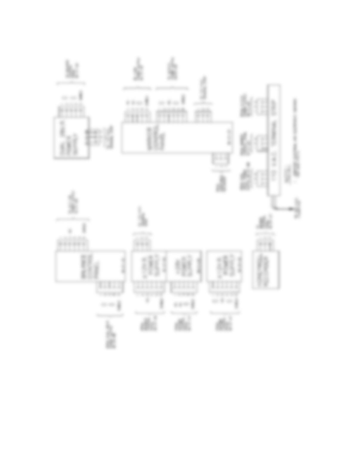
PROBLEM 20.14 Block diagram
360
PROBLEM 20.15 Block diagram
361
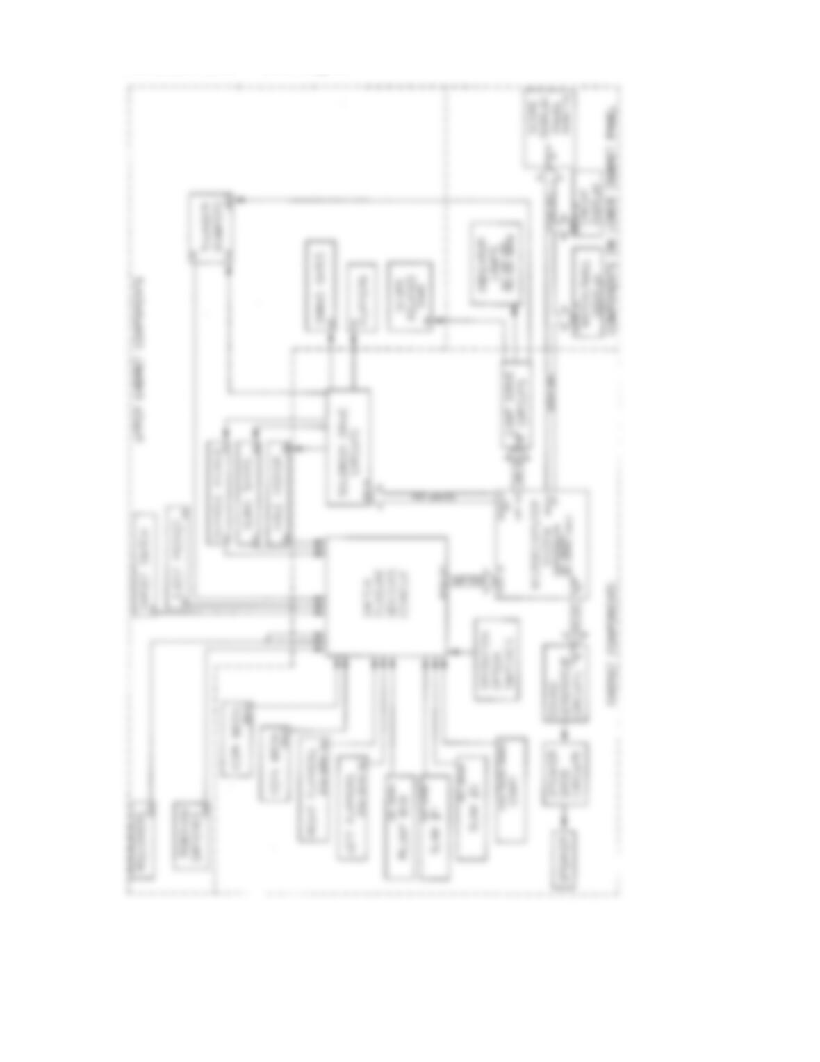
Part 3: Problems 20.16 Through 20.34
PROBLEM 20.16 Wiring harness
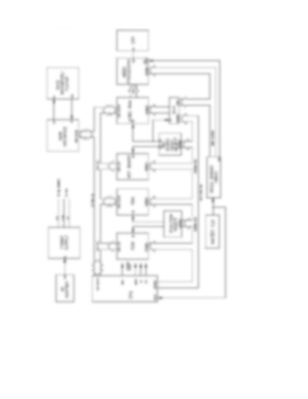
362
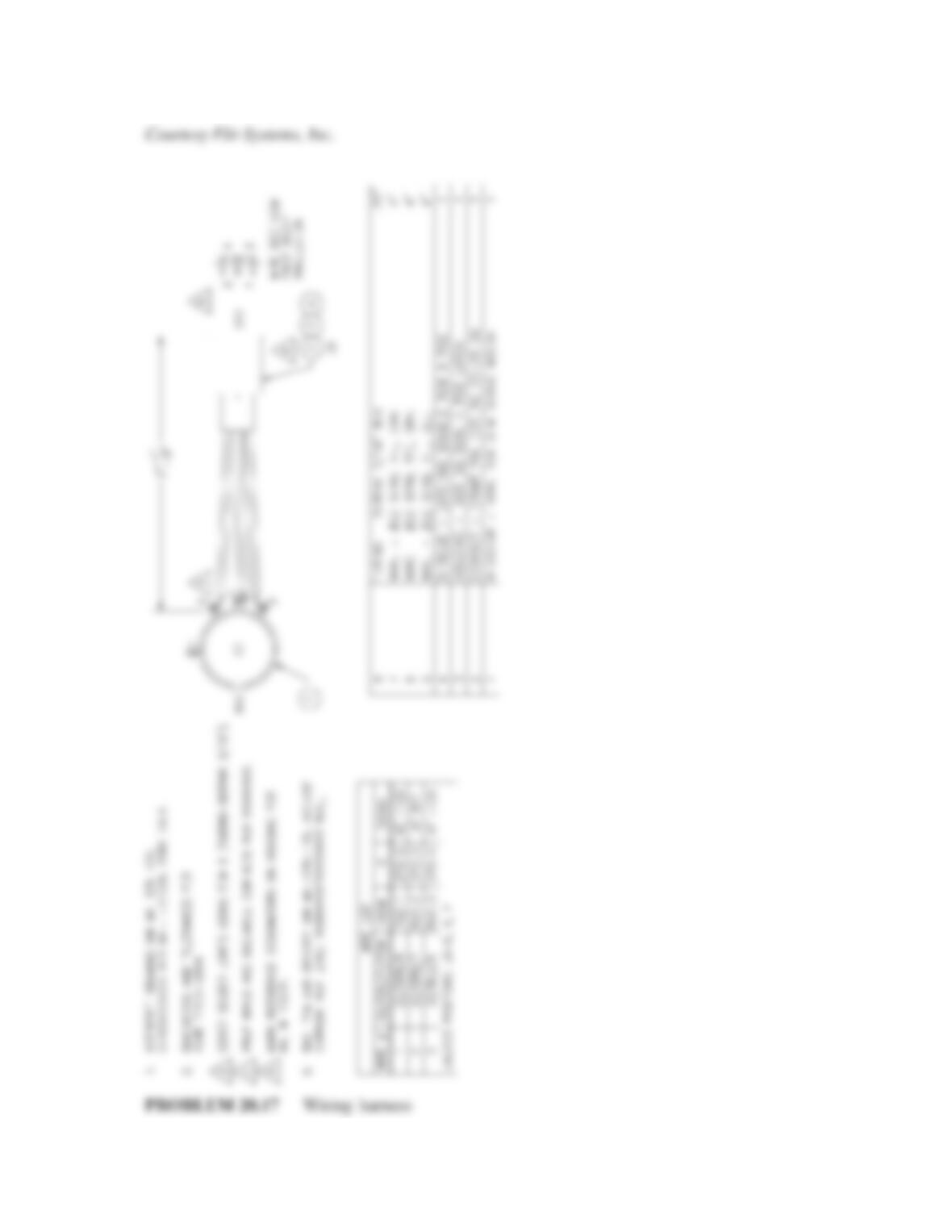
Courtesy Flir Systems, Inc.
363
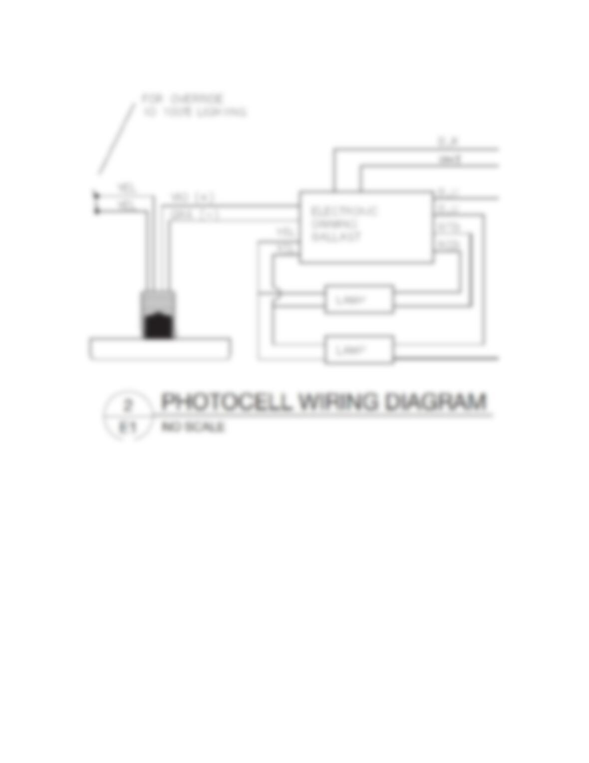
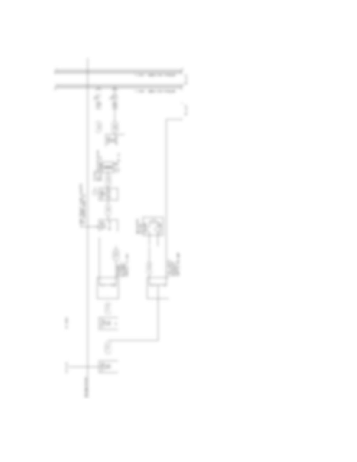
PROBLEM 20.18 Photo cell wiring diagram
364
PROBLEM 20.19 Block diagram