LAB 3-1, SEMICONDUCTOR FUNDAMENTALS
Definitions
1. Germanium: A gray-white element recovered from the ash of certain types of coal.
2. Silicon: Mineral recovered from silicon dioxide, found extensively in the earth’s crust.
3. Intrinsic material: Pure material.
4. Covalent bonding: The process of sharing valence electrons.
9. Pentavalent: Atoms with five valence electrons.
10. Trivalent: Atoms with three valence electrons.
11. Donor: An atom that gives up an electron.
12. Majority carrier: Either electrons or holes, whichever there are more of in a material.
1. Semiconductor material is doped with arsenic or other pentavalent material to provide extra
electrons in the material.
2. N-type material has extra electrons; P-type material has a deficiency in electrons.
LAB 3-2, PN JUNCTION DIODES
Definitions
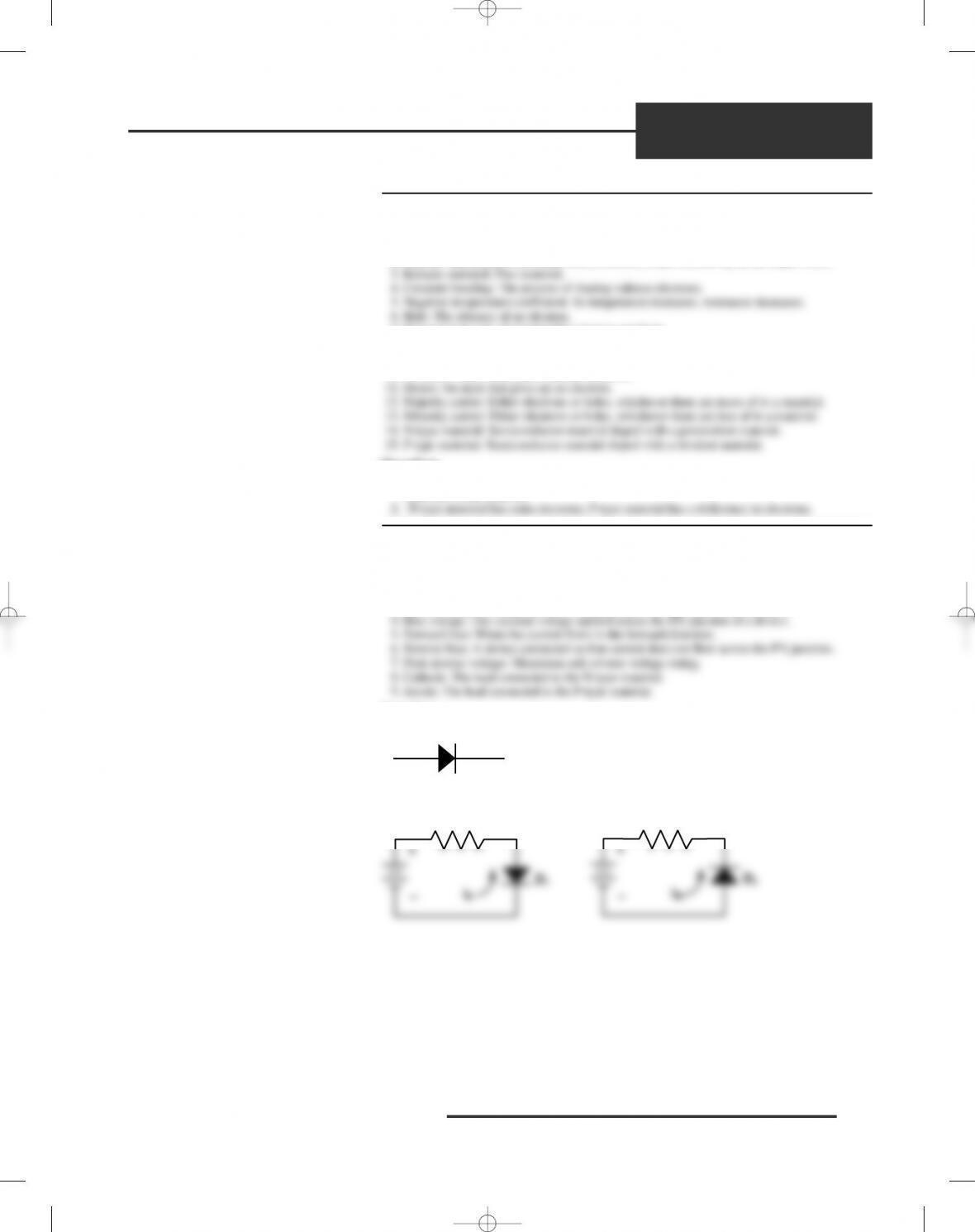
1. Diode: A semiconductor device that allows current to flow only one way.
2. Depletion region: Region near the junction of N-type and P-type material.
3. Barrier voltage: Voltage created by the junction of P-type and N-type material.
4. Bias voltage: The external voltage applied across the PN junction of a device.
5. Forward bias: When the current flows in the forward direction.
1.
2. 3.
+
–IR
RS
D1
+
–IF
RS
D1
Anode Cathode
Introduction to Electronics INSTRUCTOR’S GUIDE 69
ANSWERS
Lab Manual
28553_LM ans_rev02.qxd 4/6/11 3:32 PM Page 69
ANSWERS
Lab Manual
LAB 3-3, TESTING PN JUNCTION DIODES
Table 3-3-1
LAB 3-4, ZENER DIODES
Definitions
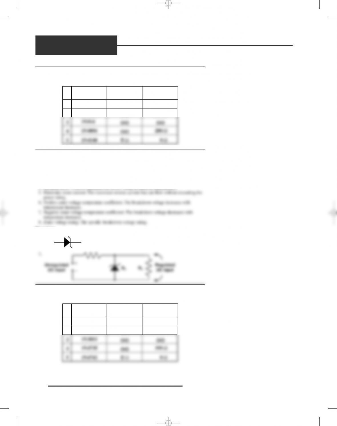
1. Zener diode: Diode designed to operate at voltages that exceed breakdown voltage.
2. Zener region: Region above breakdown, where zener diodes operate.
3. Breakdown voltage: The point at which an applied reverse voltage breaks down
and starts to conduct.
4. Derating factor: Used to determine the power rating at different temperatures.
5. Maximum zener current: The maximum reverse current that can flow without exceeding the
power rating.
1.
2.
LAB 3-5, TESTING ZENER DIODES
Table 3-5-1
Identification
Number
1
2
3
4
5
Reverse
Resistance
Forward
Resistance
1N4735
1N4742
1N3011
1N4735
1N4742
∞
∞
∞
∞
0 Ω
3308 Ω
2688 Ω
∞
399 Ω
0 Ω
–D1R1
Regulated
DC Input
Unregulated
DC Input
Anode Cathode
Identification
Number
1
2
3
4
5
Reverse
Resistance
Forward
Resistance
1N4006
1N5624
1N914
1N4006
1N4148
∞
∞
∞
∞
0 Ω
2175 Ω
1983 Ω
∞
280 Ω
0 Ω
70 Introduction to Electronics INSTRUCTOR’S GUIDE
28553_LM ans_rev02.qxd 4/6/11 3:32 PM Page 70
LAB 3-6, BIPOLAR TRANSISTORS
Definitions
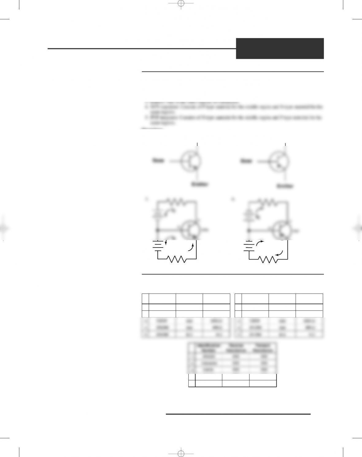
1. Bipolar transistor: A semiconductor device capable of amplifying voltage or power.
2. Base: The middle region of a transistor.
3. Emitter: One of the outer regions of a transistor.
4. NPN transistor: Consists of P-type material for the middle region and N-type material for the
1. 2.
3. 4.
LAB 3-7, TESTING BIPOLAR TRANSISTORS
See Table 3-7-1
IC
IB
IE
B
C
E
PNP
IB
IE
B
C
E
NPN
Collector
Emitter
Base
Collector
Emitter
Base
Introduction to Electronics INSTRUCTOR’S GUIDE 71
ANSWERS
Lab Manual
Identification
Number
1
2
3
4
5
Reverse
Resistance
Forward
Resistance
2N2222
Unknown
T1P29
2N1304
2N1305
∞
∞
∞
∞
0 Ω
2824 Ω
2192 Ω
∞
100 Ω
0 Ω
Identification
Number
1
2
3
4
5
Reverse
Resistance
Forward
Resistance
2N2222
Unknown
T1P29
2N1304
2N1305
∞
∞
∞
∞
0 Ω
2802 Ω
2161 Ω
100 Ω
0 Ω
3104 Ω
Identification
Number
1
2
3
4
5
Reverse
Resistance
Forward
Resistance
2N2222
Unknown
T1P29
2N1304
2N1305
∞
∞
∞
∞
∞
∞
∞
∞
∞
∞
28553_LM ans_rev02.qxd 4/6/11 3:32 PM Page 71
ANSWERS
Lab Manual
LAB 3-8, FIELD EFFECT TRANSISTORS (FETS)
Definitions
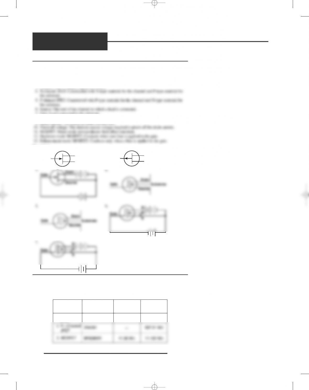
1. Junction FET: Field effect transistor that can provide amplification.
2. Substrate: Forms the base for a semiconductor device.
3. Channel: The U-shaped region of a JFET.
4. N-channel JFET: Constructed with N-type material for the channel and P-type material for
the substrate.
9. Drain current: The source-to-drain current (ID).
10. Pinch-off voltage: The drain-to-source voltage required to pinch off the drain current.
11. MOSFET: Metal oxide semiconductor field effect transistor.
1. 2.
3. 4.
S
LAB 3-9, TESTING FETS
Table 3-9-1
Gate-Source
Identification
Number
Forward
Resistance
Type Reverse
Resistance
1. N—Channel
JFET
2. P—Channel
JFET
3. MOSFET
2N3498
2N4381
BF908WR 11.38 MΩ
587.59 MΩ
567.01 MΩ
11.132 MΩ
∞
∞
S
Drain
Gate
Drain
Source
Gate
Drain
Source
Gate
72 Introduction to Electronics INSTRUCTOR’S GUIDE
28553_LM ans_rev02.qxd 4/6/11 3:32 PM Page 72
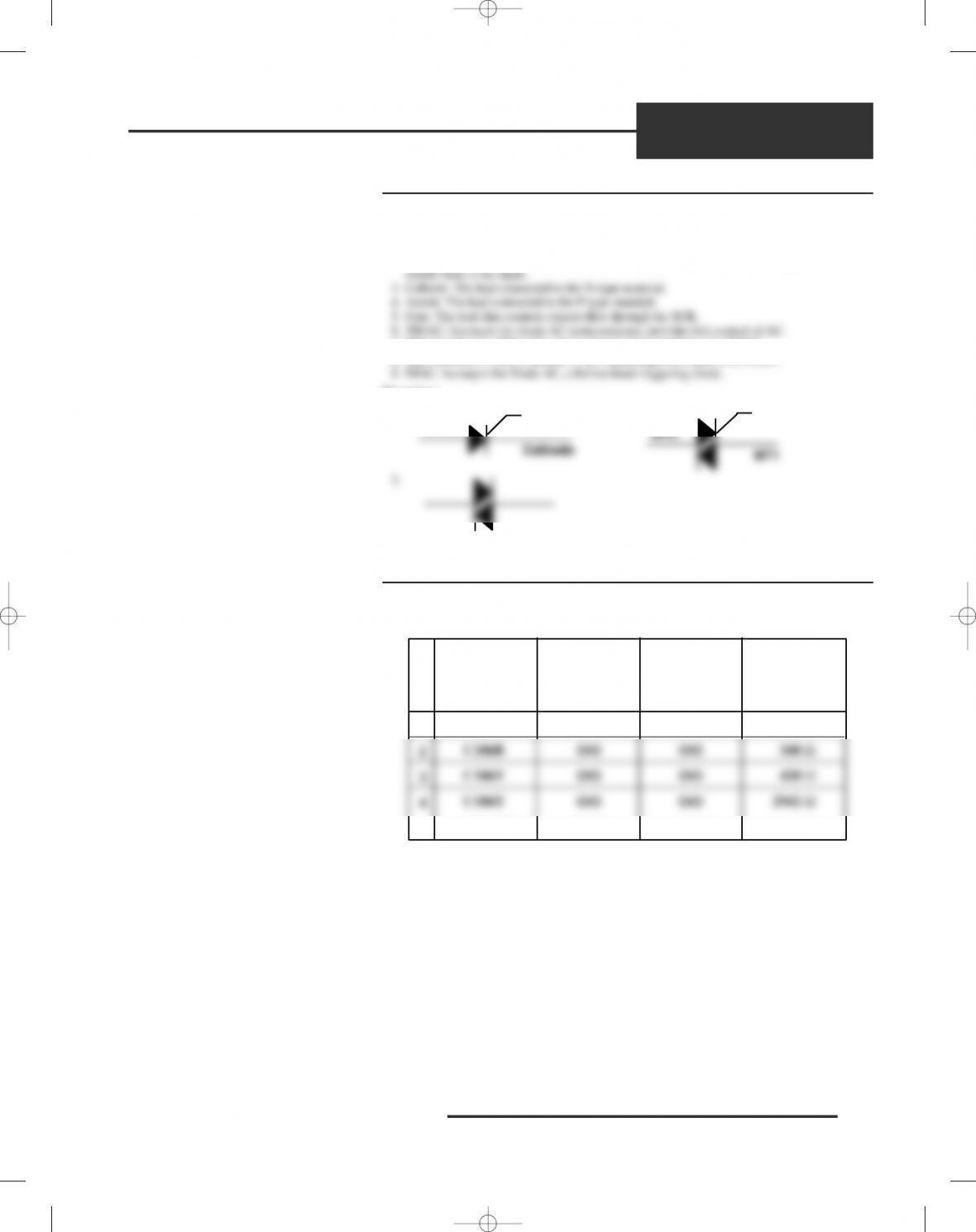
LAB 3-10, THYRISTORS
Definitions
1. Silicon controlled rectifier: A thyristor that controls current flow in only one direction.
2. Regenerative feedback: A method of obtaining an increased output by feeding part of the
output back to the input.
3. Cathode: The lead connected to the N-type material.
9. DIAC: Acronym for Diode AC, a bidirectional triggering diode.
Drawings
1. 2.
3.
LAB 3-11, TESTING SCRS
Table 3-11-1
Identification
Number
1
2
3
4
5
Reverse
Resistance
Forward
Resistance
C106B
C106B
C106Y
C106Y
GED152
∞
∞
∞
∞
69 kΩ69 kΩ
Resistance
with Gate
Short
to Anode
2726 Ω
340 Ω
2942 Ω
0 Ω
∞
∞
∞
∞
420 Ω
MT2
MT1
Gate
Anode
Cathode
Gate
Introduction to Electronics INSTRUCTOR’S GUIDE 73
ANSWERS
Lab Manual
28553_LM ans_rev02.qxd 4/6/11 3:32 PM Page 73
ANSWERS
Lab Manual
LAB 3-12, INTEGRATED CIRCUITS
Definitions
1. Integrated circuit: (IC) A complete electronic circuit in a small package.
2. Monolithic: Constructed on one plane.
3. Thin film: Constructed of a thin film of metal and oxide on a substrate of glass.
4. Thick film: Constructed using a screen-printing process.
5. Hybrid: Constructed using monolithic, thin film, thick film, and discrete components.
11. Medium scale integration: Between 100 and 1,000 transistor equivalents integrated on a
single chip of silicon.
12. Large scale integration: More than 1,000 transistor equivalents integrated on a single chip of
silicon.
1. Small, Low power consumption, Fast, Reliable, Inexpensive, Simple maintenance
2. Can not be repaired, Can not handle large currents, Internal components limited
LAB 3-13, IC IDENTIFICATION
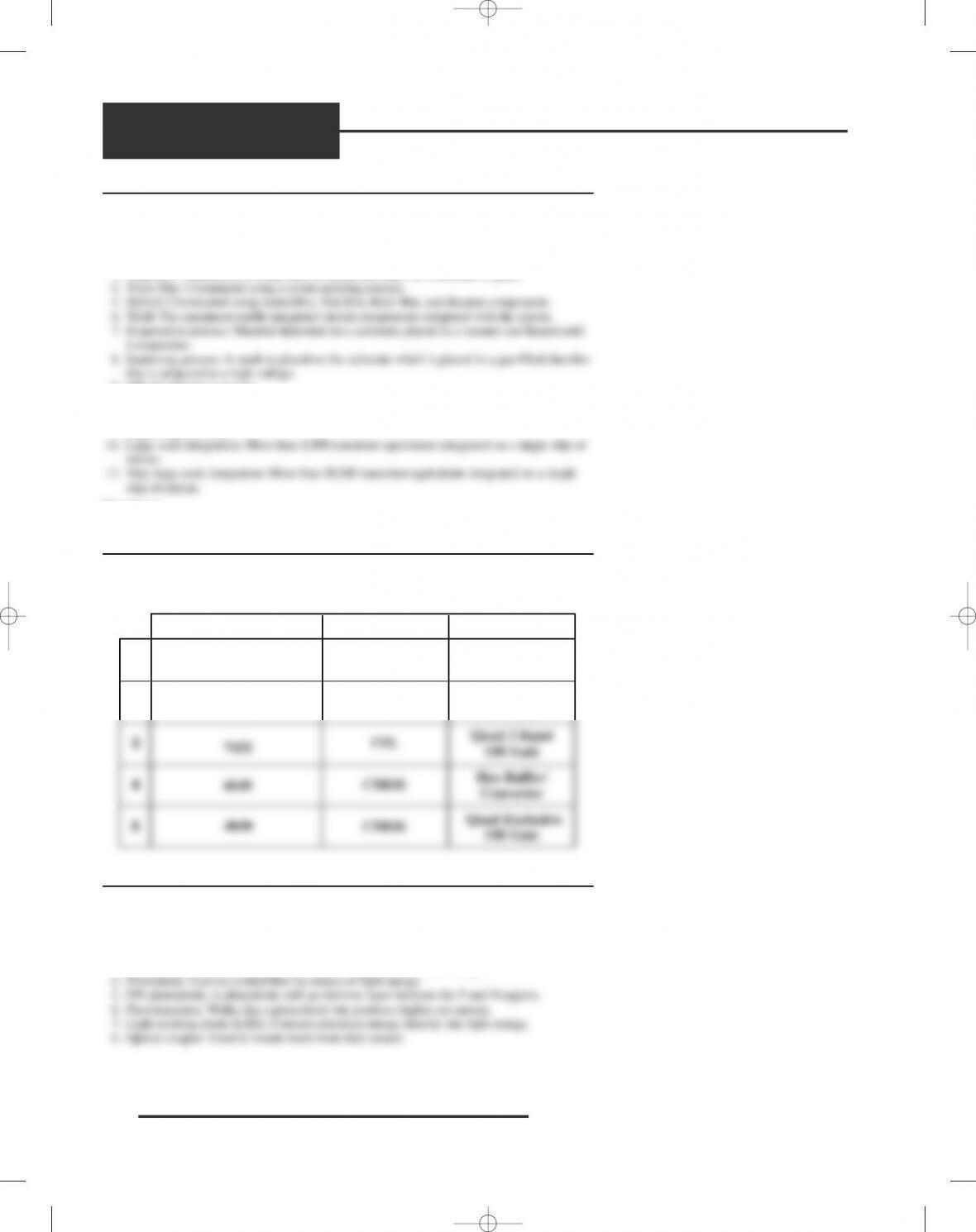
Table 3-13-1
LAB 3-14, OPTOELECTRIC DEVICES
Definitions
1. Light: Electromagnetic radiation that is visible to the human eye.
2. Photoconductive cell: Photo cell, has internal resistance that changes with light intensity.
3. Photovoltaic cell: Solar cell, converts light energy into electrical energy.
4. Photodiode: Used to control flow by means of light energy.
5. PIN photodiode: A photodiode with an intrinsic layer between the P and N regions.
IC Family TypeIdentification Number
1
2
3
4
5
IC Function
TTL
CMOS
CMOS
TTL
TTL
Quad 2 Input
NAND Gate
Quad Exclusive
OR Gate
Hex Buffer/
Converter
Quad 2 Input
OR Gate
Quad 2 Input
AND Gate
7400
7408
7432
4049
4030
28553_LM ans_rev02.qxd 4/6/11 3:32 PM Page 74
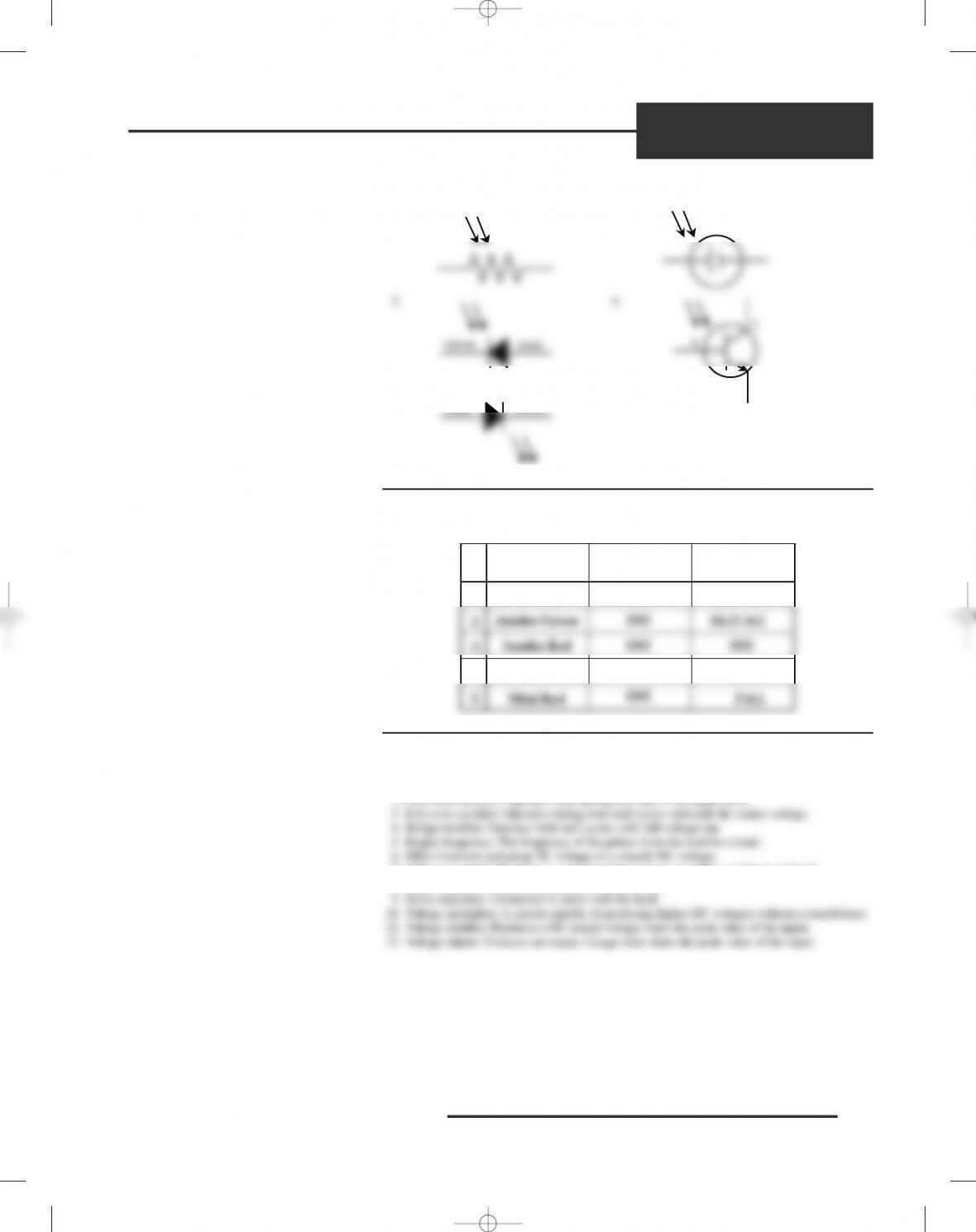
Drawings
1. 2.
3. 4.
5.
LAB 3-15, TESTING LEDS
Table 3-15-1
LAB 4-1, POWER SUPPLIES
Definitions
1. Transformer: A device for transferring energy from one circuit to another.
2. Half-wave rectifier: Operates only during one-half of the input cycle.
3. Full-wave rectifier: Operates during both half cycles with half the output voltage.
4. Bridge rectifier: Operates both half cycles with full voltage out.
9. Series regulator: Connected in series with the load.
10. Voltage multiplier: A circuit capable of producing higher DC voltages without a transformer.
Identification
Number
1
2
3
4
5
Reverse
Junction
Forward
Resistance
Jumbo Yellow
Jumbo Green
Jumbo Red
Jumbo Red
Mini Red
∞
∞
∞
∞
12.98 kΩ
14.21 kΩ
∞
10 kΩ
5 kΩ
∞
Anode Cathode
E
B
Cathode Anode
Introduction to Electronics INSTRUCTOR’S GUIDE 75
ANSWERS
Lab Manual
28553_LM ans_rev02.qxd 4/6/11 3:32 PM Page 75
ANSWERS
Lab Manual
13. Over-voltage protection circuit: Protects a load from voltage increases above a predetermined
level.
14. Fuse: A device designed to fail if an overload occurs.
15. Circuit breaker: A device that performs the same function as a fuse but does not have to be
1.
2.
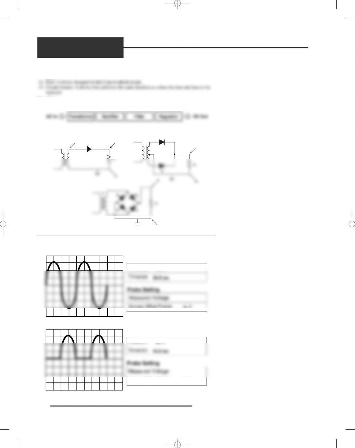
LAB 4-2, POWER SUPPLY RECTIFIERS
Figure 4-2-2
Figure 4-2-3
Time/cm
Volts/cm
Scope Setting
Across What Points
Measured Voltage
Probe Setting
45 V
16.8 ms
B, C
Time/cm
Volts/cm
Scope Setting
Across What Points
Measured Voltage
Probe Setting
90 V
16.8 ms
A, C
A B
C
D1
T1
R1
A
B
T1
D1
D2
R1
A
B
D1
D3
D2
D4
R1
T1
AC In DC Out
Transformer Rectifier Filter RegulatorRegulator
28553_LM ans_rev02.qxd 4/6/11 3:32 PM Page 76
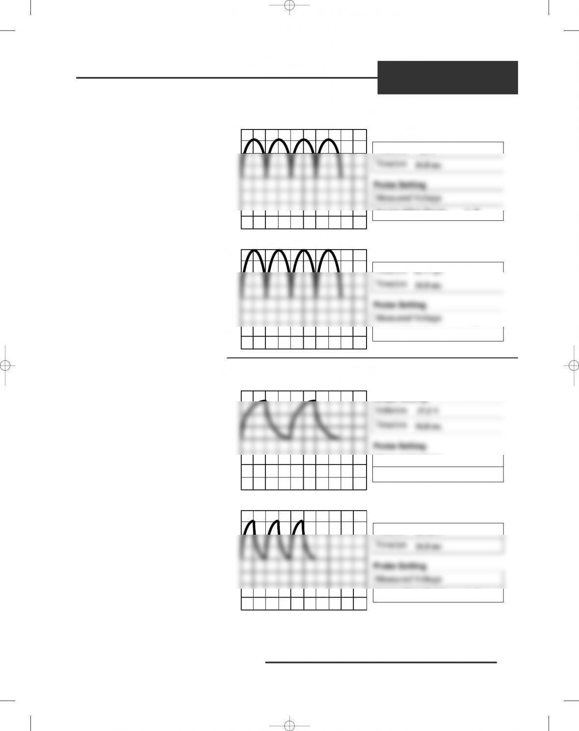
Figure 4-2-5
Figure 4-2-7
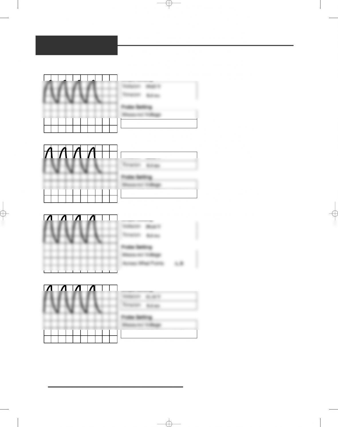
LAB 4-3, POWER SUPPLY FILTERS
Figure 4-3-2
Figure 4-3-3
Time/cm
Volts/cm
Scope Setting
Across What Points
Measured Voltage
Probe Setting
41.76 V
16.8 ms
A, B
Time/cm
Volts/cm
Scope Setting
Across What Points
Measured Voltage
Probe Setting
37.5 V
16.8 ms
A, B
Time/cm
Volts/cm
Scope Setting
Across What Points
Measured Voltage
Probe Setting
42 V (p)
16.8 ms
A, B
Time/cm
Volts/cm
Scope Setting
Across What Points
Measured Voltage
Probe Setting
21 V
16.8 ms
A, B
Introduction to Electronics INSTRUCTOR’S GUIDE 77
ANSWERS
Lab Manual
28553_LM ans_rev02.qxd 4/6/11 3:32 PM Page 77
ANSWERS
Lab Manual
Figure 4-3-5
Figure 4-3-6
Figure 4-3-8
Figure 4-3-9
Time/cm
Volts/cm
Scope Setting
Across What Points
Measured Voltage
Probe Setting
41.44 V
8.4 ms
A, B
Time/cm
Volts/cm
Scope Setting
Across What Points
Measured Voltage
Probe Setting
39.64 V
8.4 ms
A, B
Time/cm
Volts/cm
Scope Setting
Across What Points
Measured Voltage
Probe Setting
20.82 V
8.4 ms
A, B
Time/cm
Volts/cm
Scope Setting
Across What Points
Measured Voltage
Probe Setting
19.83 V
8.4 ms
A, B
28553_LM ans_rev02.qxd 4/6/11 3:32 PM Page 78
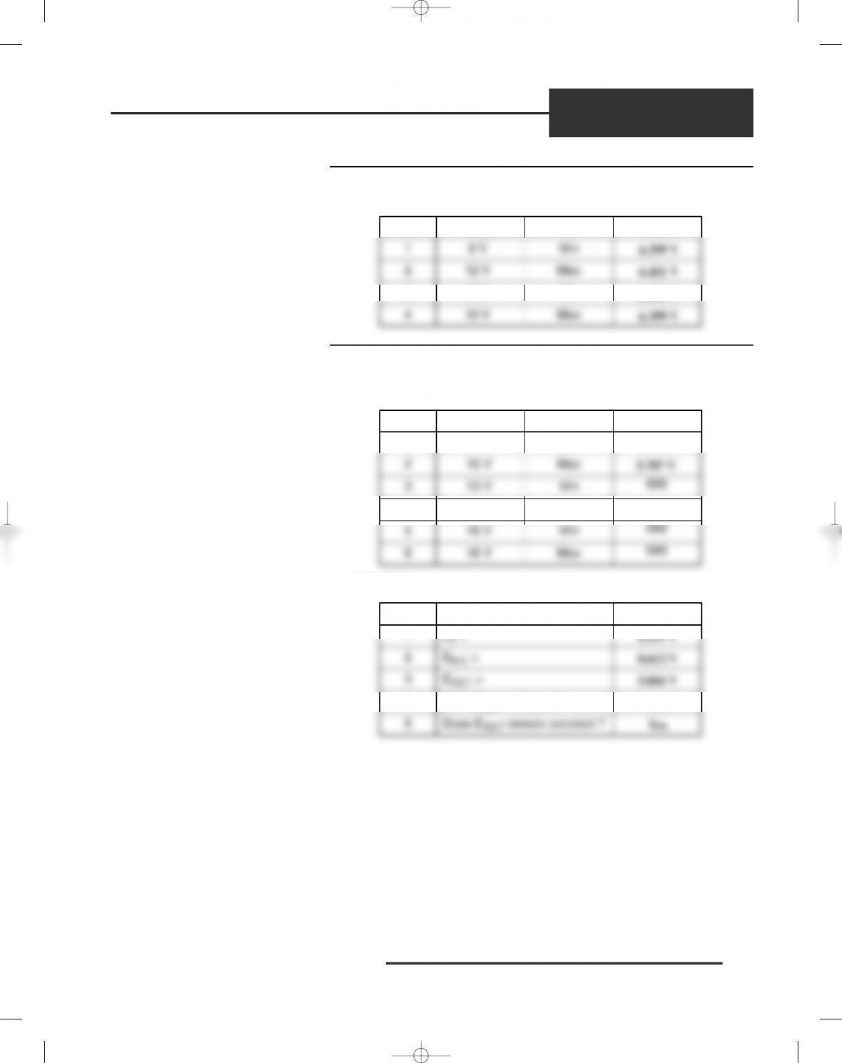
LAB 4-4, SHUNT VOLTAGE REGULATION
Table 4-4-1
LAB 4-5, SERIES VOLTAGE REGULATION:
EMITTER-FOLLOWER REGULATOR
Table 4-5-1
Table 4-5-2
EZ =
EB-E =
EOUT =
Does EOUT = EB—E ?
Step
1
2
3
4
5 Does EOUT remain constant ?
6.399 V
Yes
5.844 V
0.613 V
Yes
Question Answer
Min
Min
Min
Max
10 V
10 V
13 V
13 V
Line #
1
2
3
4
5
6
16 V
16 V
Max
Max
5.84 V
∞
∞
5.787 V
∞
∞
EIN R3EOUT
Min
Min
Max
8 V
12 V
10 V
10 V
Line #
1
2
3
4 Max
6.399 V
6.401 V
6.431 V
6.399 V
EIN R3EOUT
ANSWERS
Lab Manual
28553_LM ans_rev02.qxd 4/6/11 3:32 PM Page 79
ANSWERS
Lab Manual
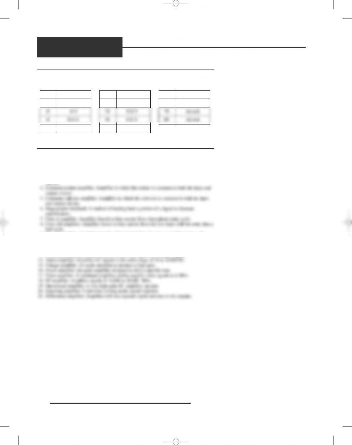
LAB 4-6, SERIES VOLTAGE REGULATION: SERIES FEEDBACK REGULATOR
Table 4-6-1
LAB 4-7, AMPLIFIERS
Definitions
1. Amplifier: Electronic circuit used to increase the amplitude of an electronic signal.
2. Amplification: Providing an output signal that is larger than the input.
3. Common-base amplifier: Amplifier in which the base is common to both the input and output
circuits.
4. Common-emitter amplifier: Amplifier in which the emitter is common to both the input and
11. Coupling: Joining of two amplifier circuits together.
12. Direct-coupled amplifier: Provides amplification of low frequencies to DC voltage.
13. Differential amplifier: Amplifier that subtracts one signal from another signal.
14. Audio amplifier: Amplifies AC signals in the audio range of 20 to 20,000 Hz.
15. Voltage amplifier: An audio amplifier to produce a high gain.
Answer
Step
5
9
Answer
Step
11
17
Answer
Step
12
5 V
9 V
6 V
6 V
32 mA
80 Introduction to Electronics INSTRUCTOR’S GUIDE
28553_LM ans_rev02.qxd 4/6/11 3:32 PM Page 80
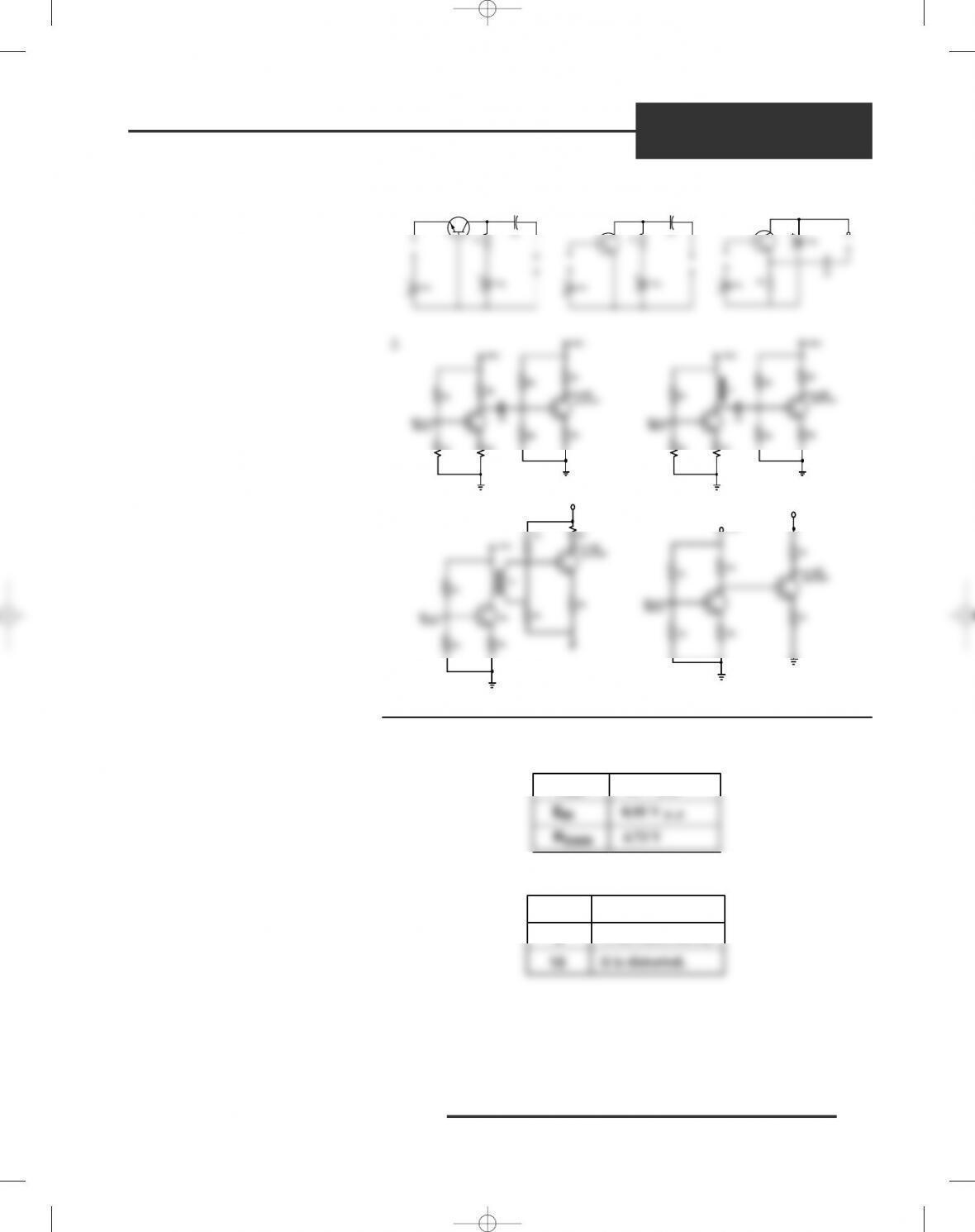
Drawings
1.
2.
LAB 4-8, COMMON EMITTER AMPLIFIER
Table 4-8-1
Table 4-8-2
Step
Answer
EIN
RGAIN
EOUT
0.95 V P–P
4.73 V
4.5 V P–P
INPUT
R1
R2
R3
R4
R5
R6
R7
R8
OUTPUT
C1
+VCC
+VCC
INPUT
R1
R2R4
R5
R6
R7
R8
OUTPUT
L1
+VCC
+VCC
C1
INPUT
R1
R2R4
Q1
+VCC
R5
R6
R7
R8
OUTPUT
+VCC
T1
INPUT
R1
R2
R3
R4
R5
R6
OUTPUT
+VCC
+VCC
VCC
CC
RL
VBB
VCC
CC
RL
VBB
VCC
CC
VBB RL
Introduction to Electronics INSTRUCTOR’S GUIDE 81
ANSWERS
Lab Manual
28553_LM ans_rev02.qxd 4/6/11 3:32 PM Page 81
ANSWERS
Lab Manual
LAB 4-9, OSCILLATORS
Definitions
1. Oscillator: A circuit that generates a repetitive AC signal.
2. Tank circuit: Formed by connecting an inductor and a capacitor in parallel.
3. Positive feedback: Feeding back a part of the output signal that is in phase.
4. Sinusoidal oscillator: Oscillator that produces sine wave outputs.
5. Crystal: Material that converts mechanical energy into electrical energy.
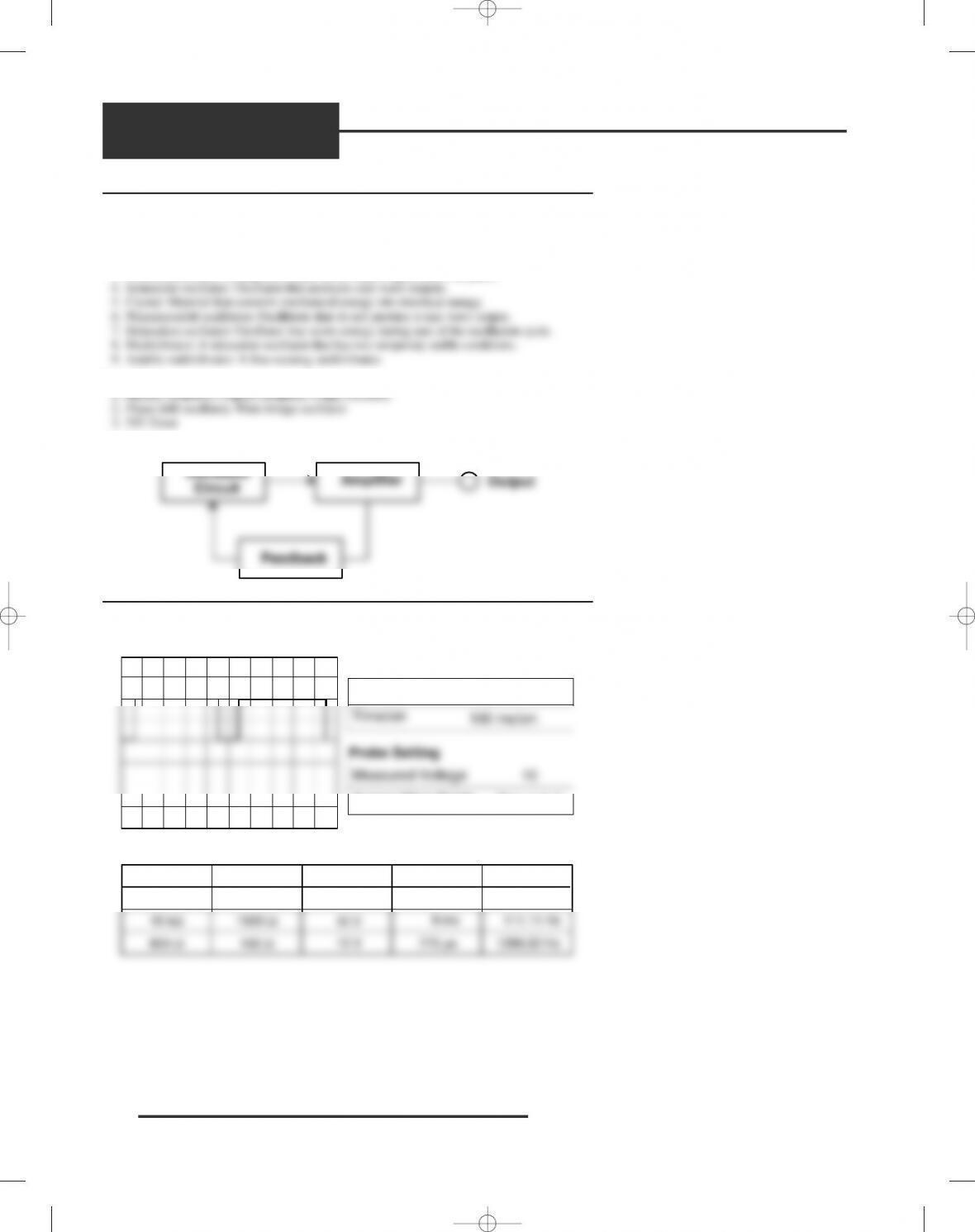
1. Hartley oscillator, Colpitts oscillator, Clapp oscillator
2. Phase shift oscillator, Wien-bridge oscillator
1.
LAB 4-10, 555 TIMER
Figure 4-10-2
Table 4-10-1
R1R2EOUT tf
68 kΩ470 kΩ
1500 Ω10 kΩ
150 Ω820 Ω
10 V
10 V
10 V
420 ms
9 ms
775 µs
2.38 Hz
1290.32 Hz
111.11 Hz
Time/cm
Volts/cm
Scope Setting
Across What Points
Measured Voltage
Probe Setting
5 V/cm
100 ms/cm
10
Pins 1 & 3
Oscillator
Circuit Amplifier Output
Feedback
28553_LM ans_rev02.qxd 4/6/11 3:32 PM Page 82