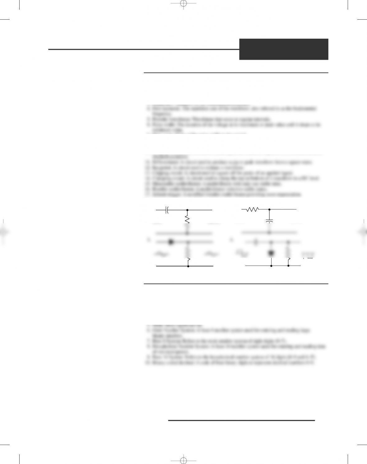
LAB 4-11, WAVESHAPING CIRCUITS
Definitions
1. Time domain: All waveforms can be changed from one shape to another using circuits.
2. Frequency domain: All period waveforms are made of sine waves.
3. Harmonics: Multiples of the fundamental frequency.
4. First harmonic: The repetition rate of the waveform; also referred to as the fundamental
frequency.
9. Undershoot: Occurs when the trailing edge of the waveform exceeds the minimum value.
10. Ringing: Dampened oscillations occurring as the transient response of a resonant circuit to
shocked excitation.
11. Differentiator: A circuit used to produce a pip or peak waveform from a square wave.
1. 2.
3. 4.
LAB 5-1, BINARY NUMBER SYSTEM
Definitions
1. Binary number system: A base 2 number system with digits 0 and 1.
2. Base 2 System: Refers to the binary number system of two digits (0–1).
3. Bit: A term derived from the words binary digit.
4. LSB: Least significant bit.
5. MSB: Most significant bit.
6. Octal Number System: A base-8 number system used for entering and reading large
OUTPUTINPUT
OUTPUTINPUT
Introduction to Electronics INSTRUCTOR’S GUIDE 83
ANSWERS
Lab Manual
28553_LM ans_rev02.qxd 4/6/11 3:32 PM Page 83
LAB 5-2, BINARY AND DECIMAL CONVERSION
Convert – binary to decimal
1. 155
10
2. 242
10
3. 85
10
4. 142
10
5. 36,710
10
1. 1 111 011
2
2. 111 011 000 000
2
3. 100 000 010 010 110
2
4. 1 000 100 111 010 110
2
5. 1 100 010 101
2
LAB 5-3, OCTAL NUMBER CONVERSION
Convert – binary to octal
1. 233
8
2. 362
8
3. 125
8
4. 216
8
1. 218
10
2. 179
10
3. 2,701
10
4. 3,156
10
1. 173
8
2. 3300
8
3. 40226
8
ANSWERS
Lab Manual
84 Introduction to Electronics INSTRUCTOR’S GUIDE
28553_LM ans_rev02.qxd 4/6/11 3:32 PM Page 84
Convert – octal to binary
1. 11 111 111
2
2. 1 000 101 010
2
3. 111 011 101 110
2
4. 101 000 111 011 100
2
LAB 5-4, HEXADECIMAL NUMBER CONVERSION
Convert – binary to hexadecimal
1. 11B
16
2. F2
16
3. 55
16
4. 8E
16
1. 930
10
2. 621
10
3. 24,159
10
4. 27,437
10
1. 7B
16
2. 6C0
16
3. 4096
16
4. 89D6
16
1. 0011 0111 1011
2
2. 0001 1010 1100 0010
2
3. 0111 0011 0101 1010
2
4. 0101 000 1101 0011 1111
2
5. 0010 1100 0110 0011 1110 0010
2
Introduction to Electronics INSTRUCTOR’S GUIDE 85
ANSWERS
Lab Manual
28553_LM ans_rev02.qxd 4/6/11 3:32 PM Page 85
ANSWERS
Lab Manual
LAB 5-5, BASIC LOGIC GATES
Definitions
1. Truth table: Summary of gate operation.
2. NOT gate: Performs the logic function of inversion; inverter.
3. AND gate: Performs the basic logic operation of multiplication.
4. OR gate: Performs the logic operation of addition.
5. NAND gate: A combination of an inverter and an AND gate.
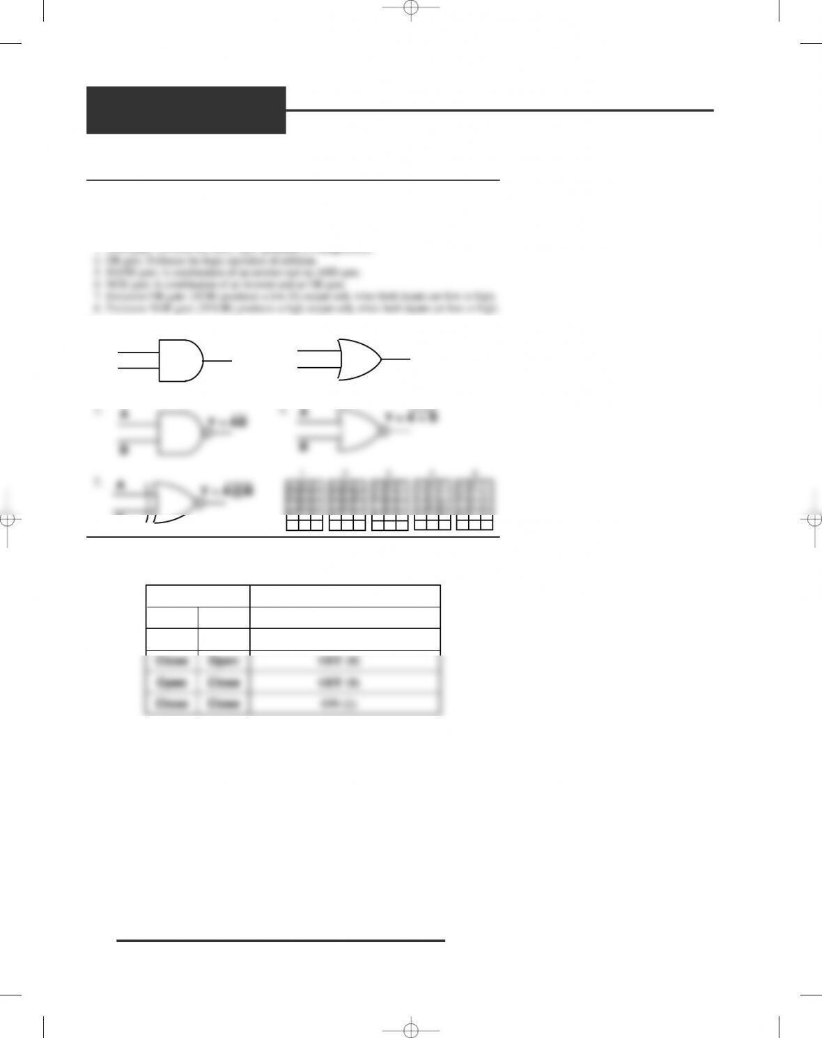
1. 2.
3. 4.
A
Y = A + B
LAB 5-6, BASIC LOGIC CIRCUITS
Table 5-6-1
Switch Position
A
Condition of Light
OFF (0) or ON (1)
B
Open Open
Close Open
Open Close
Close Close
OFF (0)
OFF (0)
OFF (0)
ON (1)
B
A
Y = A + B
AY = AB
A
B
Y = A + B
A
B
Y = AB
86 Introduction to Electronics INSTRUCTOR’S GUIDE
28553_LM ans_rev02.qxd 4/6/11 3:32 PM Page 86
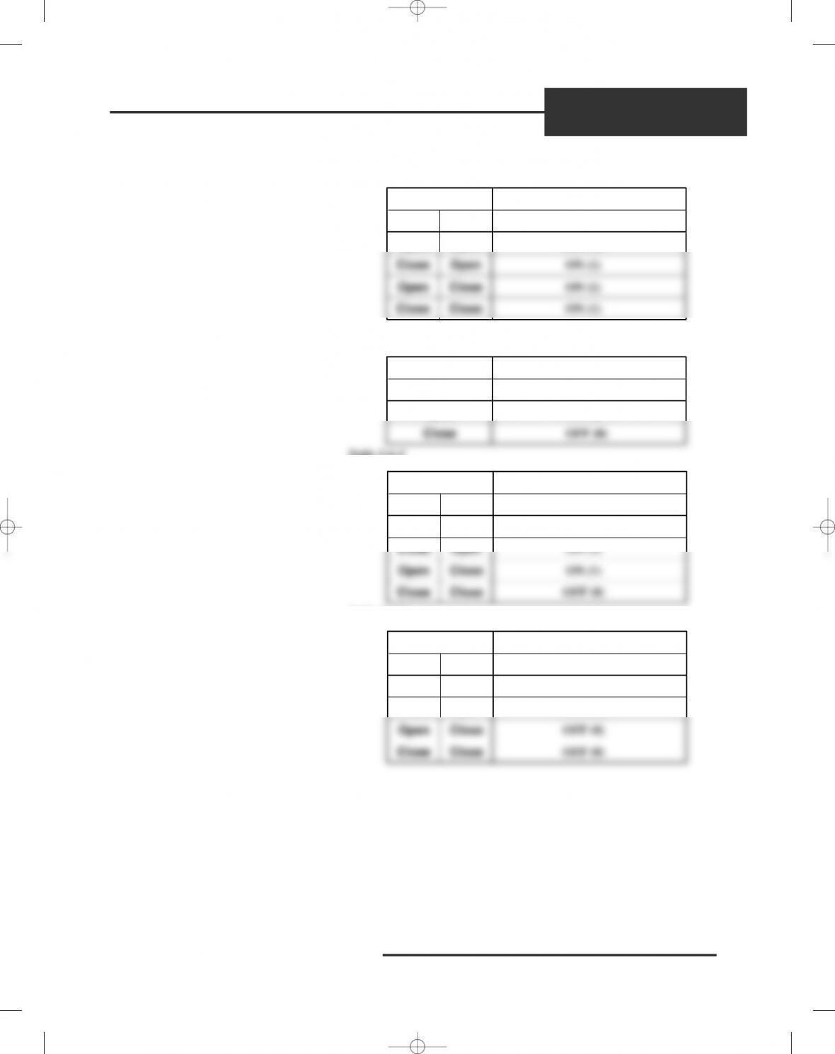
Table 5-6-2
Table 5-6-3
Table 5-6-4
Table 5-6-5
Switch Position
A
Condition of Light
OFF (0) or ON (1)
B
Open Open
Close Open
Open Close
Close Close
ON (1)
OFF (0)
OFF (0)
OFF (0)
Switch Position
A
Condition of Light
OFF (0) or ON (1)
B
Open Open
Close Open
Open Close
Close Close
ON (1)
ON (1)
ON (1)
OFF (0)
Switch Position
A
Condition of Light
OFF (0) or ON (1)
Open
Close
ON (1)
OFF (0)
Switch Position
A
Condition of Light
OFF (0) or ON (1)
B
Open Open
Close Open
Open Close
Close Close
OFF (0)
ON (1)
ON (1)
ON (1)
Introduction to Electronics INSTRUCTOR’S GUIDE 87
ANSWERS
Lab Manual
28553_LM ans_rev02.qxd 4/6/11 3:32 PM Page 87
ANSWERS
Lab Manual
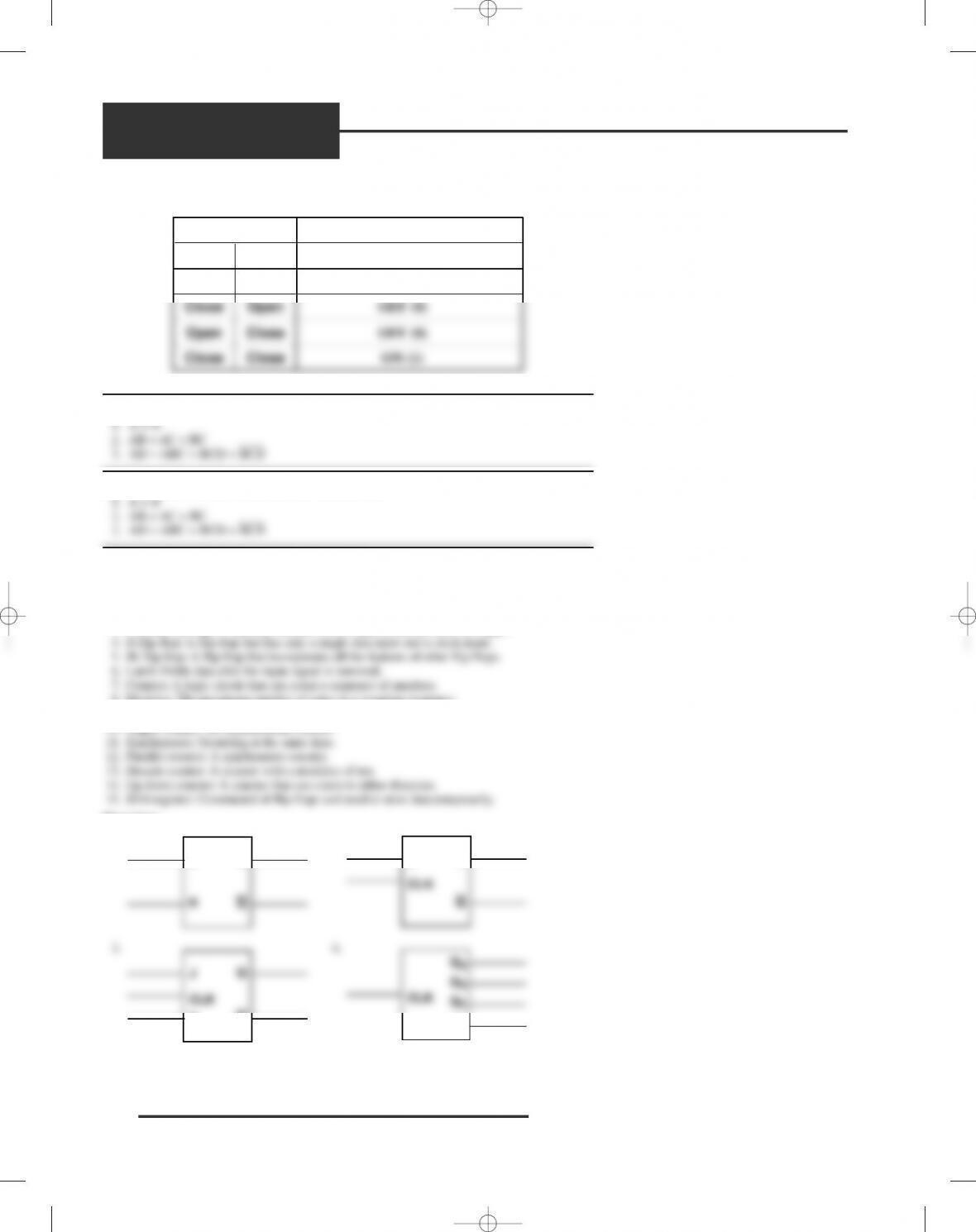
Table 5-6-6
LAB 5-7A, SIMPLIFYING LOGIC CIRCUITS
1. A + B
2. AB + AC + BC
LAB 5-7B, SIMPLIFYING LOGIC CIRCUITS
1. A + B
2. AB + AC + BC
LAB 5-8, SEQUENTIAL LOGIC CIRCUITS
Definitions
1. Flip-flop: A bistable multivibrator whose output is either a high or a low.
2. RS flip-flop: A flip-flop with a set and reset input.
3. Clocked flip-flop: A flip-flop that has a third input called the clock or trigger.
4. D flip-flop: A flip-flop that has only a single data input and a clock input.
5. JK flip-flop: A flip-flop that incorporates all the features of other flip-flops.
10. Ripple counter: An asynchronous counter.
11. Synchronous: Occurring at the same time.
12. Parallel counter: A synchronous counter.
1. 2.
3. 4.
CLK
QA
CLK
DQ
Q
R
SQ
Q
Switch Position
A
Condition of Light
OFF (0) or ON (1)
B
Open Open
Close Open
Open Close
Close Close
ON (1)
OFF (0)
OFF (0)
ON (1)
28553_LM ans_rev02.qxd 4/6/11 3:32 PM Page 88
LAB 5-9, COMBINATIONAL LOGIC CIRCUITS
Definitions
1. Encoder: A logic circuit of one or more inputs that generates a binary output.
2. Priority encoder: Receives two inputs simultaneously, generates an output according to the
highest order input.
3. Decoder: Processes complex binary codes into recognizable characters.
4. Multiplexer: Selects and routes one of several inputs to a single output.
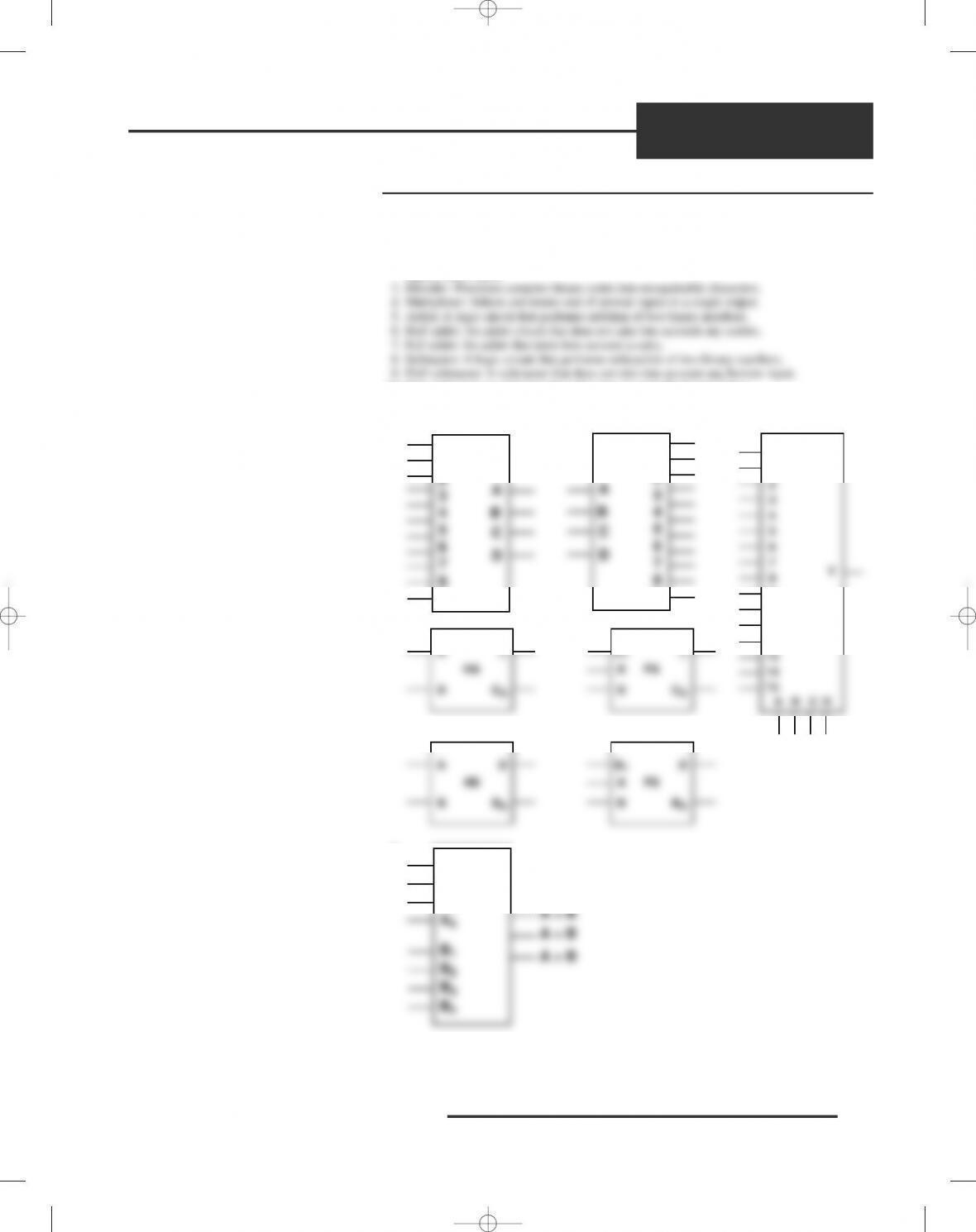
Drawings
1. 2. 3.
4.
5.
6.
A < B
A = B
A > B
A1
A2
A3
A4
B1
B2
A
B
D
BO
HS
B1
B
D
BO
FSA
A
B
∑
CO
HA
C1
B
∑
CO
FAA
0
1
2
3
4
5
6
7
8
9
10
11
12
13
14
15
Y
A B C D
0
1
2
3
4
5
6
7
8
9
A
B
C
D
0
1
2
3
4
5
6
7
8
9
A
B
C
D
ANSWERS
Lab Manual
28553_LM ans_rev02.qxd 4/6/11 3:32 PM Page 89
ANSWERS
Lab Manual
LAB 5-10, MICROCOMPUTER BASICS
Definitions
1. Digital computer: A device that automatically processes data using digital techniques.
2. Control: Decodes each instruction as it enters the computer.
3. Arithmetic logic unit: (ALU) performs math logic and decision-making operations in the
8. ROM: Random access read only memory.
9. Microprocessor: Contains ALU, timing, control, and decoding circuitry for the computer.
10. Accumulator: The most used register in a microprocessor.
11. Condition code register: A register that keeps track of the status of the microprocessor.
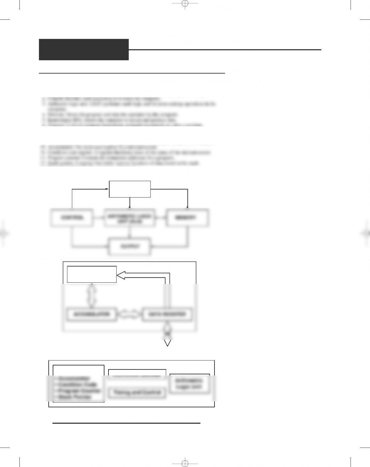
Drawings
1.
2.
3.
• Accumulator
• Condition Code
• Program Counter
• Stack Pointer
REGISTERS Instruction Decoder
Timing and Control
Logic Unit
Arithmetric
ARITHMETIC
LOGIC UNIT
ACCUMULATOR DATA REGISTER
ARITHMETIC LOGIC UNIT
TO MEMORY OR I/O
INPUT
ARITHMETIC LOGIC
UNIT (ALU) MEMORY
OUTPUT
CONTROL
90 Introduction to Electronics INSTRUCTOR’S GUIDE
28553_LM ans_rev02.qxd 4/6/11 3:32 PM Page 90
LAB 6-1, FABRICATING A PCB
Definitions
1. Printed circuit board: Consists of an insulating base material on which conductive traces of
copper act as interconnecting wires. Traces may be located on one or both sides.
2. PCB insulating base material: Supports the copper traces and is typically phenolic or epoxy
fiberglass.
3. Ferric chloride: A mild acid used to remove unwanted copper during the printed circuit board
10. Ground plane: An entire printed circuit board layer that is isolated from connections and
connected to ground potential.
11. Power plane: An entire printed circuit board layer that is isolated from connections and
connected to the voltage potential.
12. Schematic diagram: A diagram that uses symbols to represent an electrical or electronic
circuit.
13. Breadboarding: The process of constructing a temporary circuit for testing and/or modifying
a circuit design.
14. Virtual breadboarding: A surrogate environment where circuits are created by computers to
simulate the real environment to test a circuit design.
20. OSHA: Occupational Safety and Health Administration, a group that defines chemicals with
hazardous substances.
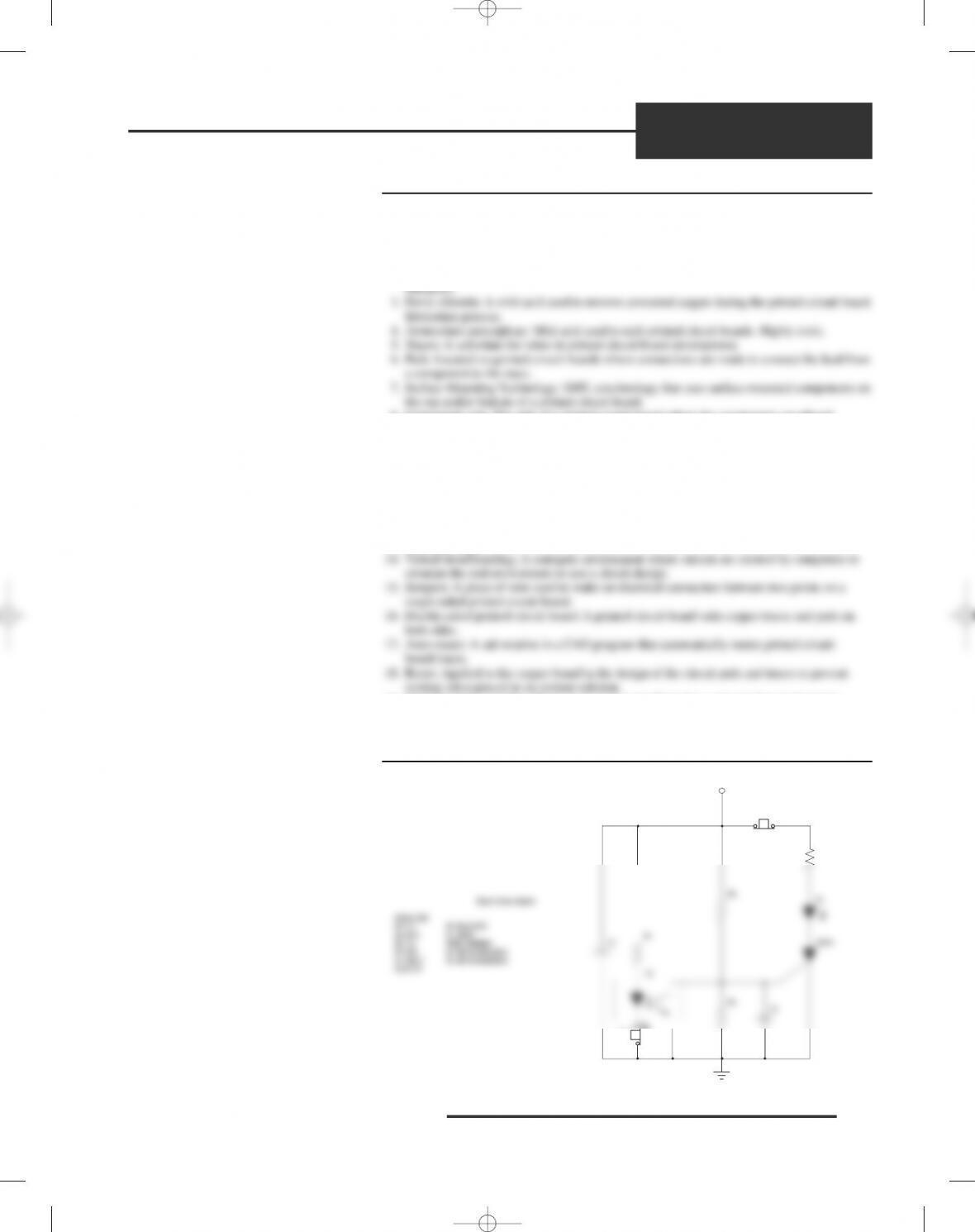
LAB 6-2, SCHEMATIC DIAGRAMS
1.
Introduction to Electronics INSTRUCTOR’S GUIDE 91
ANSWERS
Lab Manual
+
9-12 V
Reset
Trigger
C1
R1
U1
R2
R3
C2
SCR1
D1
R4
S2
S1
Open Door Alarm
Parts List
R1 1 k D1 Red LED
R2 10 k U1 4N25
R3 1 k SCR1 2N5064
R4 470 S1 NC Pushbutton
C1 100 F S2 NC Pushbutton
C2 0.1 F
28553_LM ans_rev02.qxd 4/6/11 3:32 PM Page 91
ANSWERS
Lab Manual
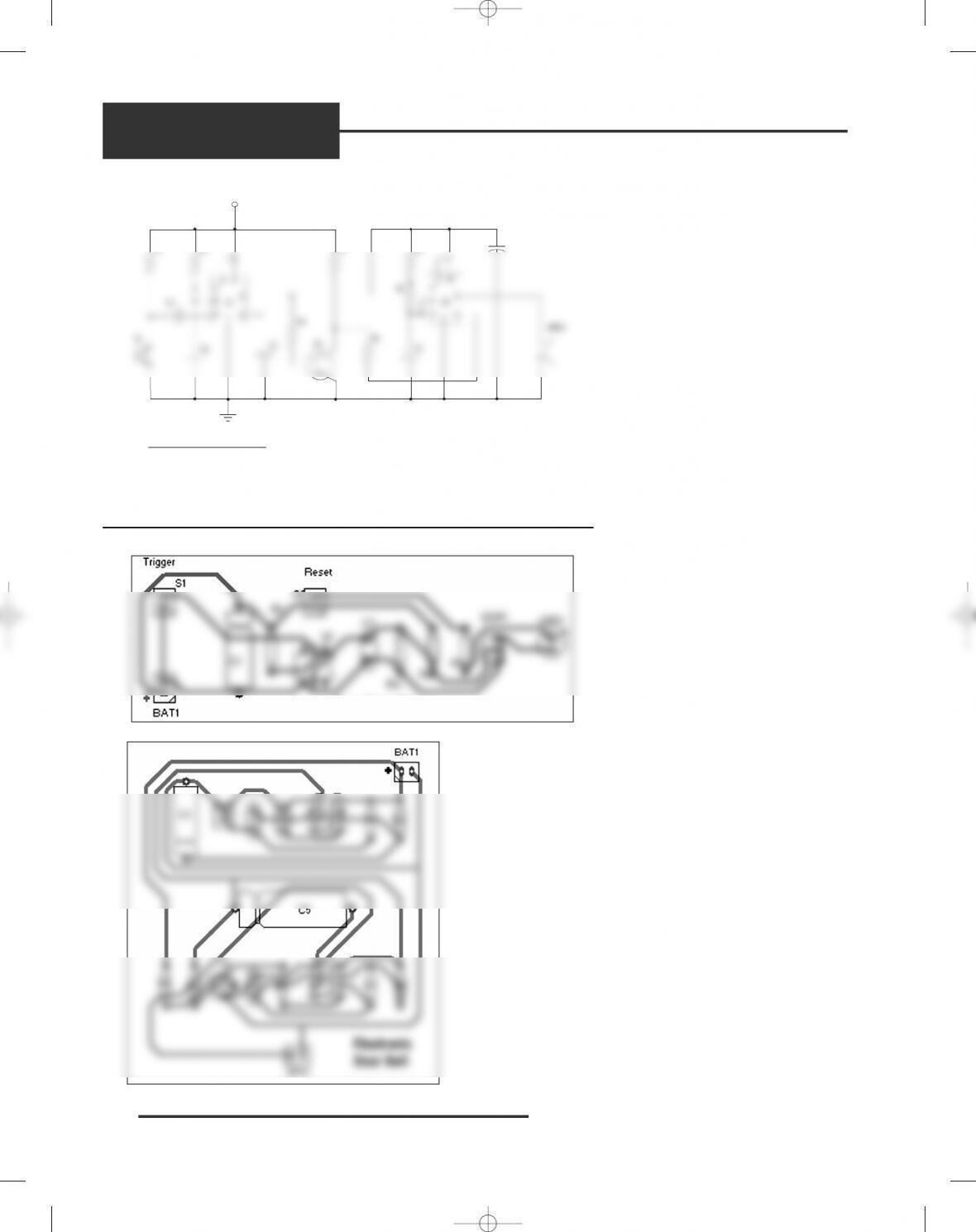
2.
LAB 6-3, PCB FABRICATION
1.
2.
92 Introduction to Electronics INSTRUCTOR’S GUIDE
+9-12V
1
2
3
4
5
6
7
8
U1
1
2
3
4
5
6
7
8
U2
Electronic Door Bell
Parts List
R1 10 kΩ C1 0.01 µF
R2 100 kΩ C2 10 µF
R3 10 kΩ C3 0.01 µF
R4 1 kΩ C 4 0.01 µF
R5 100 kΩ C5 470 µF
R6 1 kΩ U 1, U2 LM555
R7 47 kΩ Q1 2N2222A
SPK1 8 Ω Speaker
R1R2
C1
R3
R4R6
C5
SPK1
S1R5
Q1
R7
Open Door Alarm
Electronic
Door Bell
28553_LM ans_rev02.qxd 4/15/11 3:14 PM Page 92
LAB 6-4, ETCH AND FINISH A PCB
1. a. Transfer original artwork to the back of the graph paper using a light table.
b. Label the transferred design “BOTTOM.”
c. Clean the copper surface of the copper-clad board.
d. Wrap the artwork toward the copper side with the artwork identified “BOTTOM” facing out.
b. Draw the design from the component side and reverse it to form the solder side.
c. Print out a positive image on transparency film or a toner transfer system.
d. Clean the copper surface of the copper-clad board.
e. Lay the copied image on the copper side of the board with the toner side down.
f. Align as necessary and apply heat and pressure.
LAB 6-5, PCB ASSEMBLY AND REPAIR
1. Printed circuit board holder: Holds a printed circuit board while it is being assembled or
repaired.
2. Illuminated magnifier: Provides a means of detecting improper connections or broken traces
on a printed circuit board.
3. Isolated power supply: Isolates the circuit under test from ground to prevent electrical shock.
4. Multimeter: A meter that combines a voltmeter, ammeter, and ohmmeter.
5. 10X Oscilloscope probe: A probe that multiplies the voltage setting of an oscilloscope by ten.
6. Function generator: Capable of generating sine waves, triangular waveforms, and square
waveforms.
12. Leg warmer: Pieces of insulation used on LEDs and small transistors to avoid overheating.
13. Soldering: The joining of component leads to a printed circuit board or terminals using
solder.
14. Defluxer: A chemical substance that is used to dissolve flux to aid in its removal from a
printed circuit board.
15. Desoldering wick: Uses a copper braid with flux and heat to create capillary action to pull up
molten solder.
16. Surface mount technology: A technology that uses surface mounted components on the top
and/or bottom of a printed circuit board.
17. Properly soldered connection: A solder connection that displays a smooth, well feathered at
the edges, bright and shiny with a slight concave configuration.
Introduction to Electronics INSTRUCTOR’S GUIDE 93
ANSWERS
Lab Manual
28553_LM ans_rev02.qxd 4/6/11 3:32 PM Page 93
ANSWERS
Lab Manual
LAB 6-6, ASSEMBLING A PCB
1. a. Wipe the soldering tip on a damp sponge.
b. Tin the tip by applying solder to it.
c. Apply the tip to both the component lead and pad.
d. Apply solder to the back of the connection.
e. Remove the solder.
f. Remove the tip from the connection.
1
e. Install and solder SCR
1
.
f. Install and solder S
2
and connect and solder S
1
.
g. Trim all leads flush to the printed circuit board.
h. Verify all components are installed properly and correctly oriented.
1
g. Trim all leads flush to the printed circuit board.
h. Verify all components are installed properly and correctly oriented.
LAB 6-7, ELECTRONICS TOOL BOX
1. G
2. R
3. B
12. I
13. O
14. M
LAB 6-8
1. Schematic diagram: A diagram that uses symbols to represent an electrical or electronic
circuit.
2. Ohmmeter: A meter used to measure resistance.
3. Voltmeter: A meter used to measure the voltage between two points in a circuit.
zero ohm resistance.
8. Open circuit: A component or trace in a circuit that has infinite resistance resulting in no
94 Introduction to Electronics INSTRUCTOR’S GUIDE
28553_LM ans_rev02.qxd 4/6/11 3:32 PM Page 94
9. a. Visually check the circuit thoroughly.
b. Power circuit and check for any defects.
c. Troubleshoot any defects to determine what is wrong, why it’s wrong, and what needs to
c. Resistors changing value through aging or circuit defects.
d. Traces shorted to another trace or opened.
11. Use pill bottles, film canisters, egg cartons, and/or ice cube trays.
Introduction to Electronics INSTRUCTOR’S GUIDE 95
ANSWERS
Lab Manual
28553_LM ans_rev02.qxd 4/6/11 3:32 PM Page 95

28553_LM ans_rev02.qxd 4/6/11 3:32 PM Page 96