Exam
Name___________________________________
MULTIPLE CHOICE. Choose the one alternative that best completes the statement or answers the question.
1)
One characteristic of a voltage follower is its ________.
1)
A)
large voltage gain
B)
high output impedance
C)
non–inversion
D)
phase inversion
2)
If an op–amp’s output increases 8 V every 12 µs in response to a step input voltage, the slew rate
equals ________.
2)
A)
96 V/µs
B)
0.75 V/µs
C)
0.667 V/µs
D)
1.5 V/µs
3)
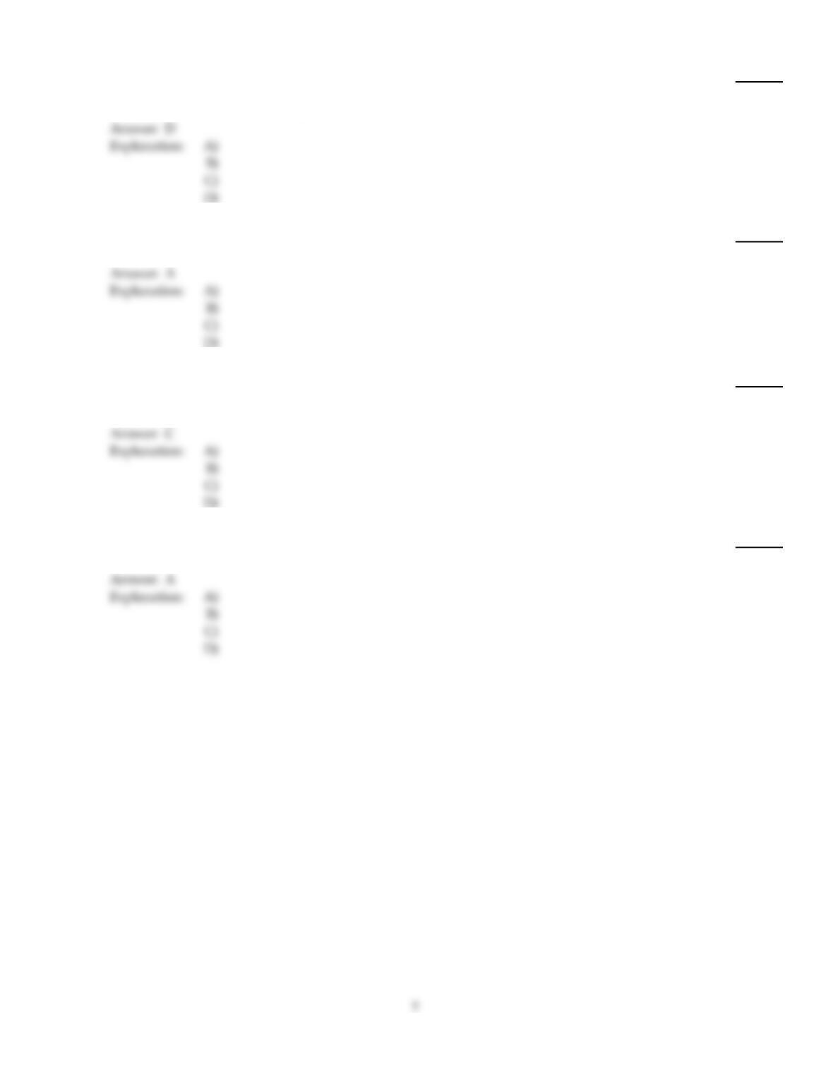
The circuit in Figure 18–1(c) is known as the ________.
3)
A)
non–inverting amplifier
B)
voltage follower amplifier
C)
open–loop amplifier
D)
inverting amplifier
4)
VRF equals ________ in Figure 18–1(c).
4)
A)
VRI
B)
VCC
C)
VOUT
D)
VIN
5)
A diff–amp with two out–of–phase signal voltages applied to the two inputs is called:
5)
A)
differential input.
B)
differential output.
C)
phase inverter output.
D)
phase inverter input.
A
6)
If Rf= 1.2 M and AV= 120 in Figure 18–1(c), Ri equals ________.
6)
A)
10 k
B)
1 k
C)
120
D)
100 k
A
7)
The op–amp configuration with the highest possible input impedance is:
7)
A)
differential op–amp.
B)
voltage–follower op–amp.
C)
inverting op–amp.
D)
non–inverting op–amp.
B
C
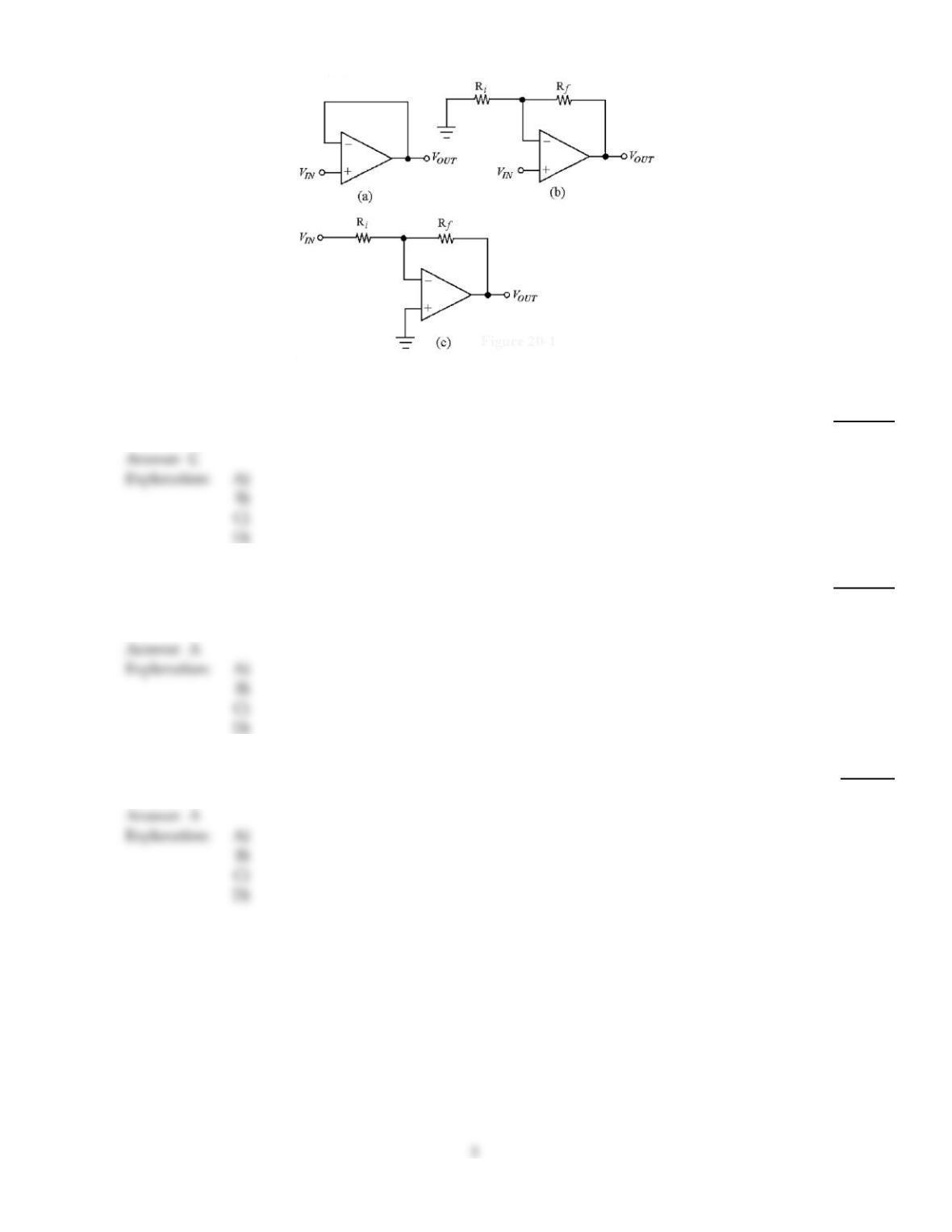
Figure 18–1
8)
If Rf= 150 k and Ri= 2.2 k in Figure 18–1(c), the voltage gain equals ________.
8)
A)
–69.2
B)
–1
C)
–68.2
D)
infinite
9)
Which of these amplifiers provides a high input resistance and a variable gain?
9)
A)
non–inverting amp with a rheostat as Rf.
B)
voltage–follower amp
C)
open–loop amp
D)
inverting amp
A
10)
The feedback attenuation of a voltage follower op–amp is:
10)
A)
= 1.
B)
> 1.
C)
Rf/Ri.
D)
< 1.
A
C
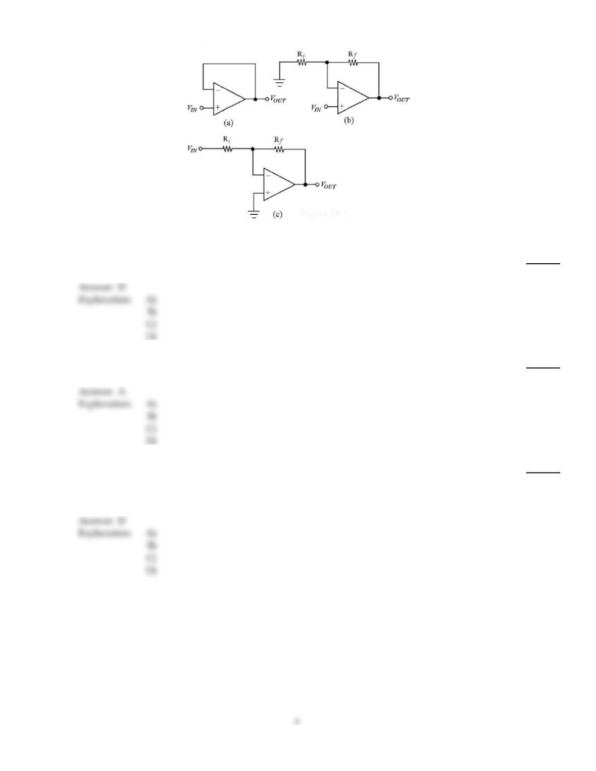
Figure 18–1
11)
If Rf= 1.2 M and Ri= 47 k in Figure 18–1(b), the voltage gain equals ________.
11)
A)
25.5
B)
25
C)
26
D)
26.5
12)
If Rf= 0.5 M and Ri= 10 k in Figure 18–1(b), the voltage gain equals ________.
12)
A)
51
B)
6
C)
50
D)
5
13)
To build an amplifier with a 10 K input impedance and a voltage gain of 41, use the ________
amplifier, Ri= ________, Rf= ________.
13)
A)
non–inverting, 40 k, 200 k
B)
non–inverting, 10 k, 410 k
C)
inverting, 10 k, 200 k
D)
inverting, 10 k, 410 k
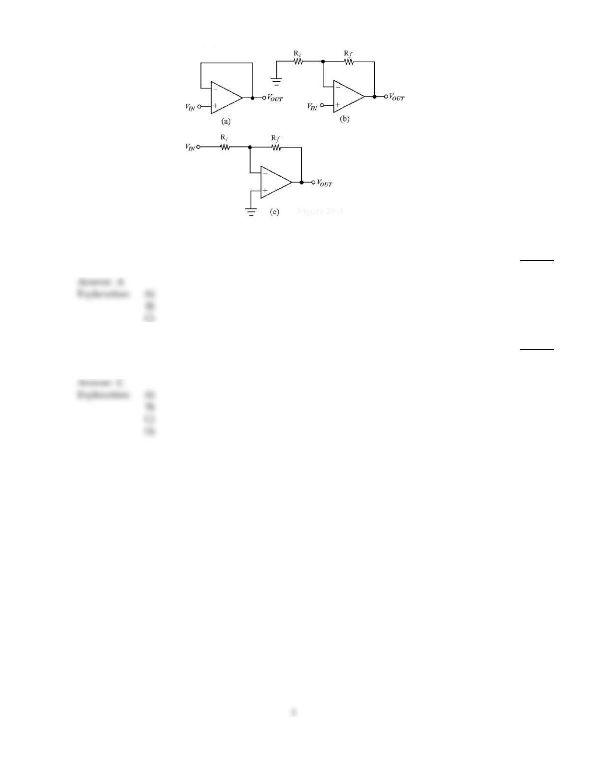
Figure 18–1
14)
The input impedance of the amplifier in Figure 18–1(b) is ________.
14)
A)
very high.
B)
about 10 k
C)
very low
15)
The distinguishing characteristic of the voltage follower configuration is:
15)
A)
non–inverting output.
B)
very high input impedance.
C)
voltage gain of unity.
D)
all of the above
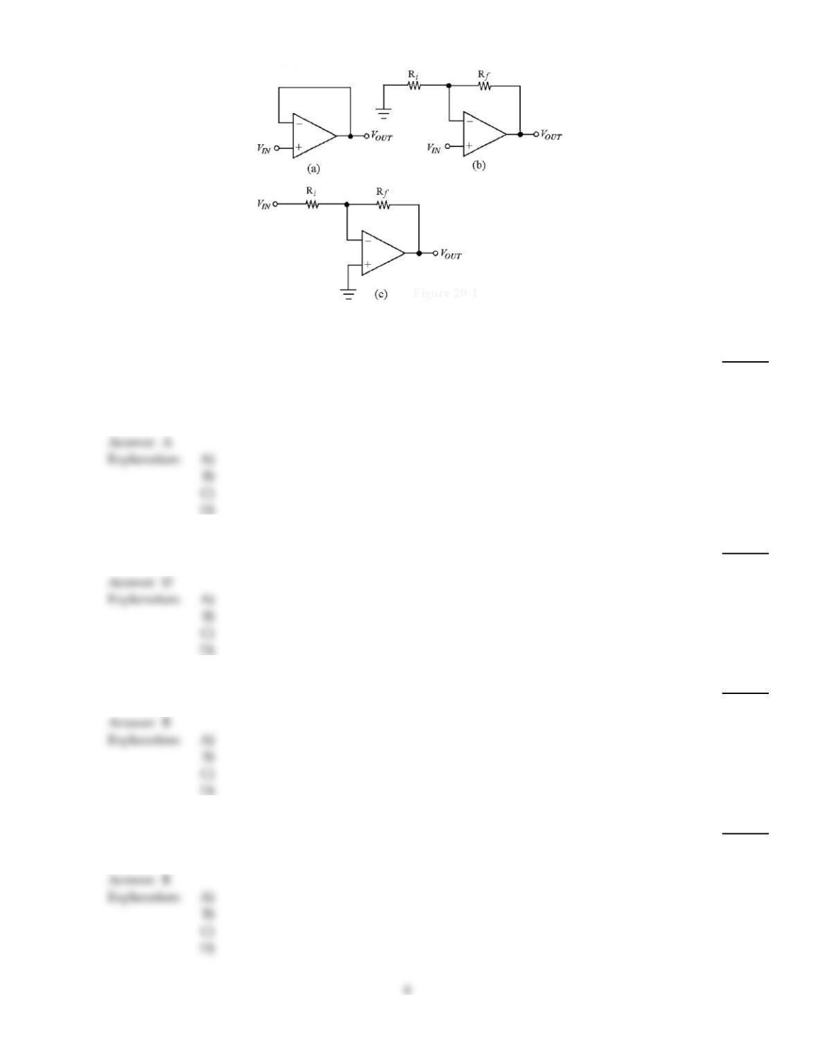
Figure 18–1
16)
What trouble in the amplifier in Figure 18–1(c) could cause the output voltage to clip severely?
16)
A)
The input signal is too large.
B)
The power is off.
C)
The amplifier’s gain is too low.
D)
The input signal is too small for the amplifier to respond.
17)
Identify the open–loop amplifier in Figure 18–1.
17)
A)
Figure 18–1(a)
B)
Figure 18–1(b)
C)
Figure 18–1(c)
D)
none of these
18)
Identify the non–inverting amplifier in Figure 18–1.
18)
A)
Figure 18–1(a)
B)
Figure 18–1(b)
C)
Both A and B
D)
Neither of these
19)
If you know an op–amp’s open–loop gain only, you can determine the closed–loop gain of:
19)
A)
an inverting op–amp.
B)
a voltage follower op–amp.
C)
an non–inverting op–amp.
D)
all of these.
20)
A practical differential amplifier provides:
20)
A)
very high input impedance.
B)
very high differential voltage gain > 1000.
C)
very small common mode gain < 1.
D)
all of these.
21)
Which one of these op–amp terminals provides an output that is in–phase with the input?
21)
A)
non–inverting
B)
inverting
C)
offset null
D)
VCC
22)
Which one of these devices produces amplifiers with characteristics close to those of an ideal
amplifier?
22)
A)
BJT
B)
JFET
C)
Op–amp
D)
MOSFET
23)
If Ri= 2.2 k, Rf= 220 k and AOL = 25,000 in an inverting op–amp, ACL equals ________.
23)
A)
–100
B)
–250
C)
–0.01
D)
100
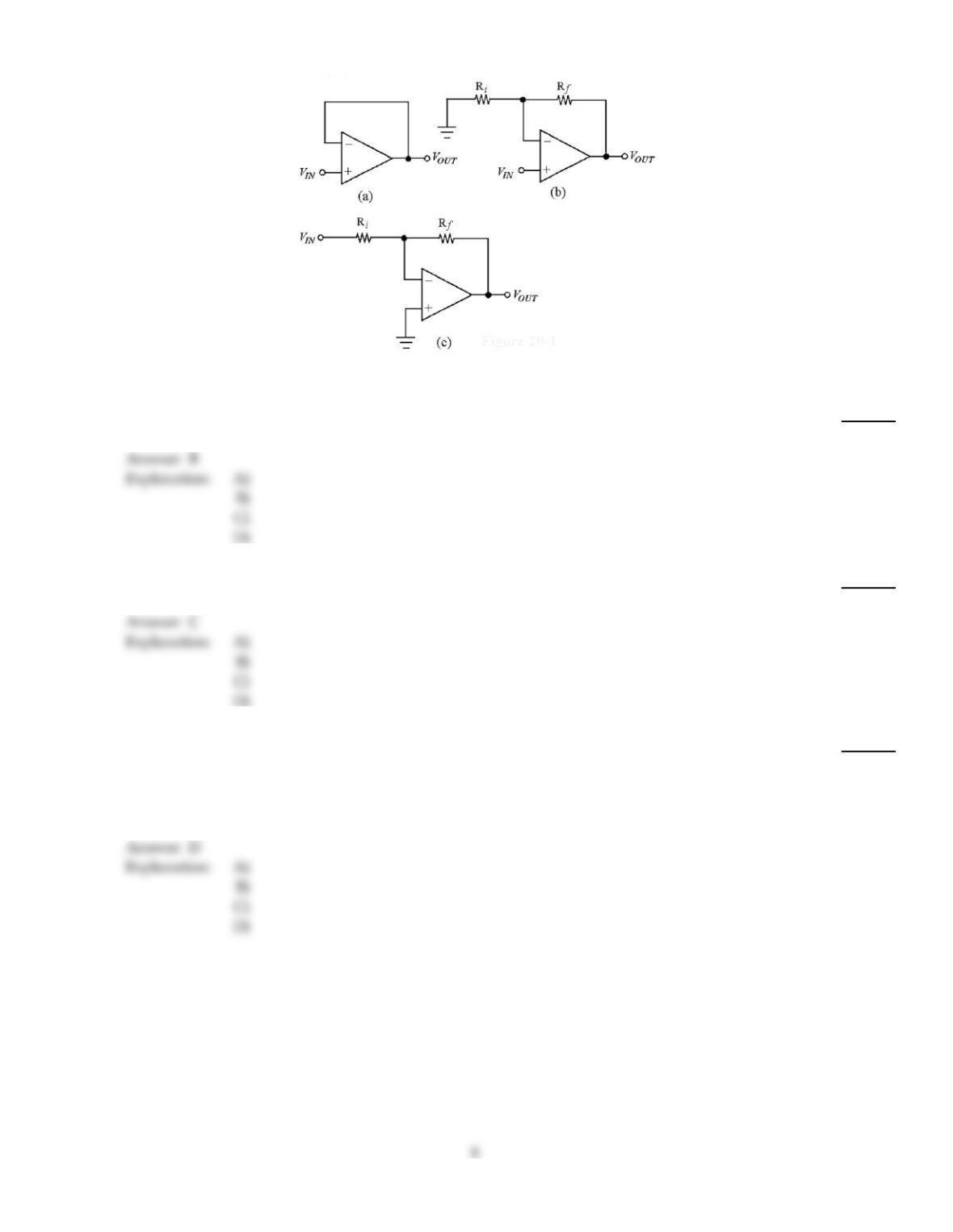
Figure 18–1
24)
If Rf= 470 k and Ri= 5 k in Figure 18–1(b), the voltage gain equals ________.
24)
A)
470
B)
95
C)
1.01
D)
94
25)
A typical op–amp has ________ input impedance and ________ output impedance.
25)
A)
low, high
B)
high, high
C)
high, low
D)
low, low
26)
A CMRR of 10,000 means that the op–amp provides that:
26)
A)
the differential input is greatly amplified.
B)
Av(d)/Acm = 10,000.
C)
the common mode input is greatly reduced.
D)
all of these.
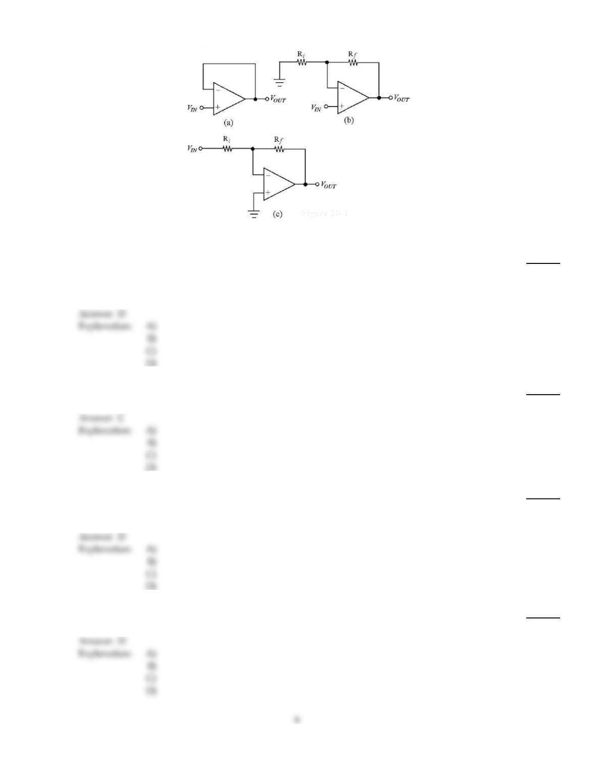
Figure 18–1
27)
What trouble in the amplifier in Figure 18–1(b) could cause the voltage between the inverting and
non–inverting inputs to nearly equal 0 V?
27)
A)
Ri is open.
B)
The power is off.
C)
Rf is open.
D)
There is no problem; 0 V is normal.
28)
If Ri= 4.7 k and Rf= 0.18 M in Figure 18–1(c), the voltage gain equals ________.
28)
A)
–39.3
B)
–1
C)
–38.3
D)
infinite
29)
What trouble in the amplifier in Figure 18–1(c) could cause the voltage gain to drop to 1?
29)
A)
Rf is open
B)
Ri is open
C)
VOUT is grounded
D)
the power is off
30)
If Rf= 100 k and AV= (–833) in Figure 18–1(c), Ri equals ________.
30)
A)
10 k
B)
100 k
C)
1 k
D)
120
31)
A CMRR of 90,000 equals a decibel CMRR of ________.
31)
A)
90,000 dB
B)
–99 dB
C)
99 dB
D)
91 dB
32)
If Rf= 5 k and Ri= 10 k in Figure 18–1(c), the voltage gain equals ________.
32)
A)
–2
B)
–0.5
C)
0
D)
–5
33)
Which one of these characteristics do an op–amp and a MOSFET have in common?
33)
A)
high input impedance
B)
high voltage gain
C)
high current gain
D)
high CMRR
34)
If Ri= 1 k, Rf= 100 k and VOUT = 5 V in a noninverting op–amp, VRI equals ________.
34)
A)
500 mV
B)
49.5 mV
C)
495 mV
D)
50 mV
35)
If Ri= 1 k, Rf= 100 k and VOUT = 5 V in a noninverting op–amp, ACL equals ________.
35)
A)
99
B)
0.0099
C)
1
D)
101
36)
If Rf= 333 k and Ri= 22 k in Figure 18–1(b), the voltage gain equals ________.
36)
A)
15.1
B)
15
C)
16.1
D)
16
37)
If an op–amp’s output increases 6 V every 18 µs in response to a step input voltage, the slew rate
equals ________.
37)
A)
0.99 V/µs
B)
33 V/µs
C)
3 V/µs
D)
0.33 V/µs
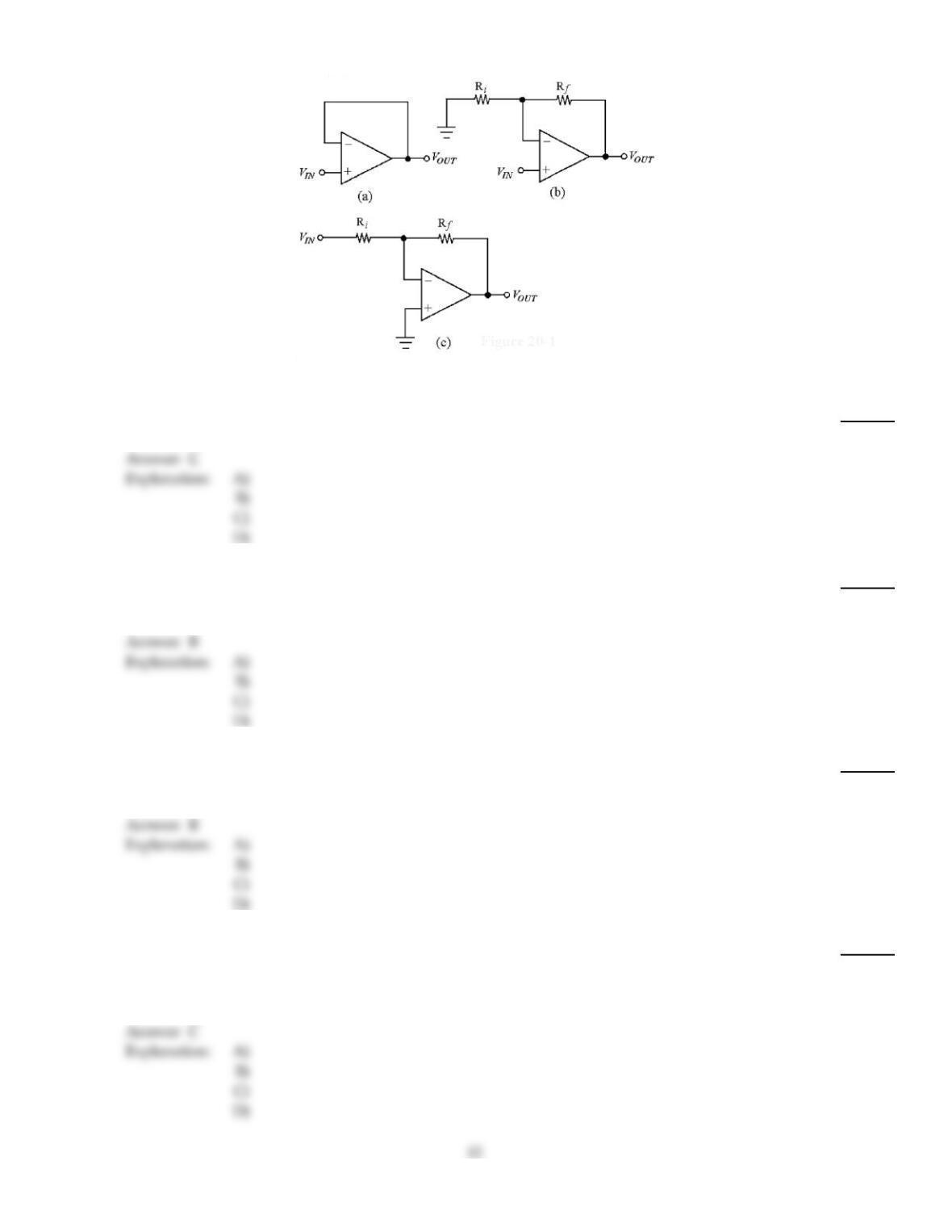
Figure 18–1
38)
If Rf= 100 k and Ri= 6.8 k in Figure 18–1(c), the voltage gain equals ________.
38)
A)
–15.7
B)
–1
C)
–14.7
D)
infinite
39)
To use an op–amp as a buffer, use the ________.
39)
A)
inverting amplifier
B)
voltage follower amplifier
C)
differential amplifier
D)
non–inverting amplifier
40)
A diff–amp with 1 input grounded and the signal voltage applied only to the other input is called:
40)
A)
grounded input.
B)
single ended.
C)
single input.
D)
single output.
41)
To build an amplifier with a 5 K input impedance and a voltage gain of 40, use the ________
amplifier, Ri= ________, Rf= ________.
41)
A)
non–inverting, 40 k, 200 k
B)
non–inverting, 5 k, 40 k
C)
inverting, 5 k, 200 k
D)
inverting, 5 k, 2 k
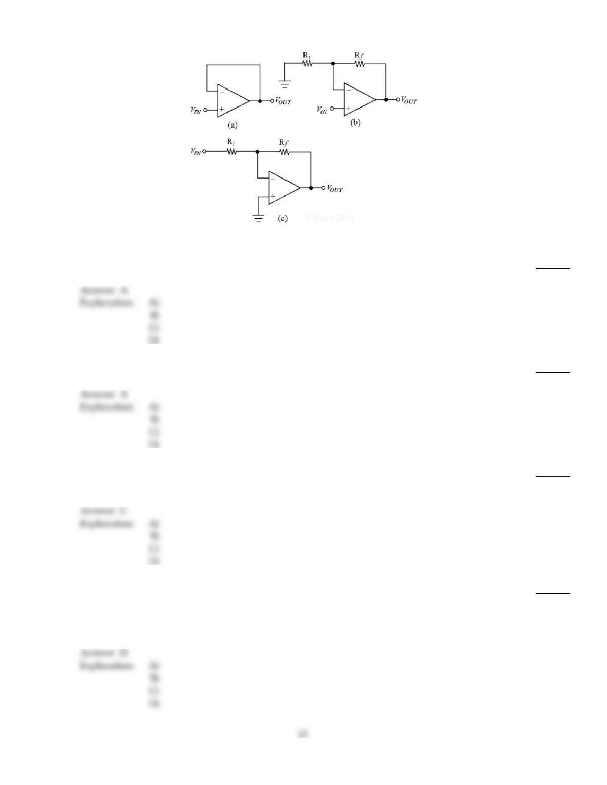
Figure 18–1
42)
What is the voltage gain of the amplifier in Figure 18–1(a)?
42)
A)
1
B)
1000
C)
100,000
D)
10
43)
Which of the amplifiers in Figure 18–1 would be used as a buffer amplifier?
43)
A)
Figure 18–1(a)
B)
Figure 18–1(b)
C)
Figure 18–1(c)
D)
none of these
A
44)
The circuit in Figure 18–1(a) is used as a(n) ________.
44)
A)
inverting amplifier
B)
oscillator
C)
buffer amplifier
D)
high gain amplifier
C
45)
One characteristic of a noninverting amplifier is a ________.
45)
A)
high output impedance
B)
voltage gain of one
C)
very low input impedance
D)
voltage gain slightly more than an inverting amplifier with the same values
D
A
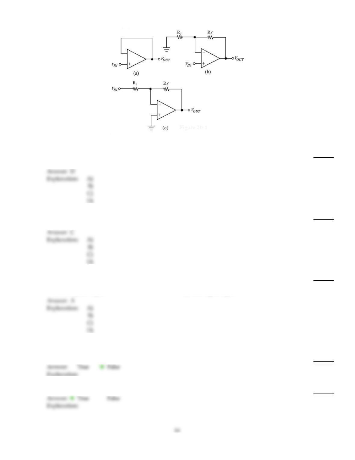
Figure 18–1
46)
If Rf= 150 k and Ri= 10 k in Figure 18–1(c), the voltage gain equals ________.
46)
A)
–0.066
B)
–1
C)
–16
D)
–15
47)
A CMRR of 35,000 equals a decibel CMRR of ________.
47)
A)
–91 dB
B)
88 dB
C)
91 dB
D)
35000 dB
48)
A diff–amp with two identical signal voltage applied to the two inputs is called:
48)
A)
common mode input.
B)
common mode output.
C)
same phase input.
D)
same signal input.
TRUE/FALSE. Write ‘T’ if the statement is true and ‘F’ if the statement is false.
49)
Differential amplifiers provide high voltage gain and low common–mode rejection.
49)
50)
A typical value of input bias current for an op–amp is around 80 nA.
50)
51)
An op–amp’s CMRR is usually expressed in dB.
51)
52)
The ideal amplifier has infinite gain, infinite input impedance, and zero output impedance.
52)
53)
Practical op–amps come reasonably close to the requirements for an ideal amplifier.
53)
54)
A voltage–follower op–amp has a voltage gain greater than one.
54)
55)
The slew rate of an op–amp is determined by the frequency response of the internal amplifiers.
55)
56)
The open–loop voltage gain of an op–amp is very large.
56)
57)
An op–amp with a low CMRR easily rejects noise signals that appear at both inputs.
57)
58)
An op–amp’s input offset voltage, VOS, is the differential input voltage required to make the
differential output voltage zero.
58)
Answer Key
Testname: C18
Answer Key
Testname: C18
17