46)
Which one of these characteristics is found in a common–collector amplifier?
46)
A)
a current gain of one
B)
a low input resistance
C)
a very high power gain
D)
a high input resistance
47)
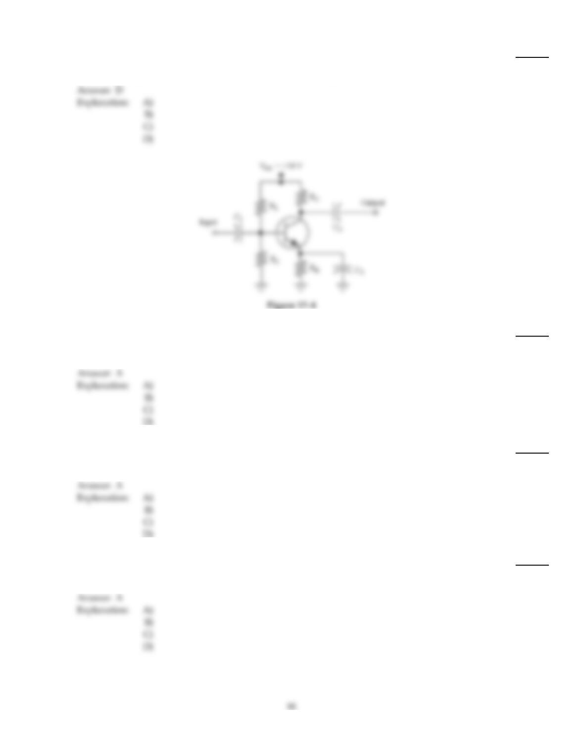
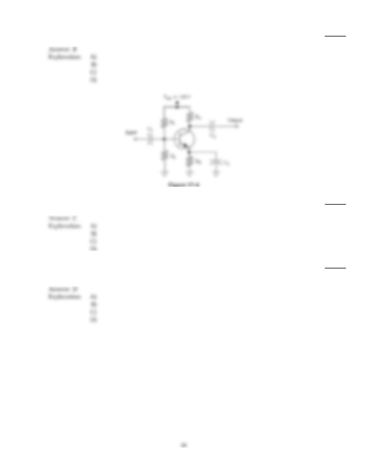
If the base–emitter junction opens in Figure 17–4, VC ________.
47)
A)
increases to VCC
B)
decreases to VE
C)
decreases to 0 volts
D)
does not change
48)
What type of amplifier normally has a voltage gain of one?
48)
A)
common–drain
B)
common–mode
C)
common–emitter
D)
common–source
49)
Crossover distortion occurs in a ________ amplifier when the amplifier is biased at ________.
49)
A)
push–pull, cutoff
B)
common–source, cutoff
C)
push–pull, saturation
D)
common–emitter, saturation
50)
If a BJT amplifier is operated as a switch that is off, this operating condition is known as ________.
50)
A)
saturation
B)
thermal runaway
C)
VP
D)
cutoff
51)
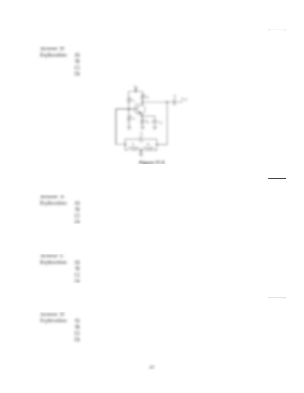
If the value of C1 increases in Figure 17–5, the circuit ________.
51)
A)
operates at a lower frequency
B)
operates at dc
C)
operates at a higher frequency
D)
does not change at all
52)
If C1 opens in Figure 17–5, the circuit will probably ________.
52)
A)
continue to operate normally
B)
increase its oscillating frequency
C)
stop oscillating entirely
D)
decrease its oscillating frequency
53)
The output signal of a CE amplifier is always ________.
53)
A)
in–phase with the input signal
B)
equal to the input signal
C)
larger than the input signal
D)
out–of–phase with the input signal
54)
In all FETs, the drain current equals the ________ current.
54)
A)
gate
B)
source
C)
collector
D)
emitter
55)
Which voltage would indicate that the amplifier in Figure 17–4 is operating in saturation?
55)
A)
VC= 18 V
B)
VBE = 9 V
C)
VCE = 0.15 V
D)
VBE = 0.7 V
56)
For normal operation of a NPN transistor, the base must be ________.
56)
A)
positive with respect to the collector
B)
disconnected
C)
negative with respect to the emitter
D)
positive with respect to the emitter
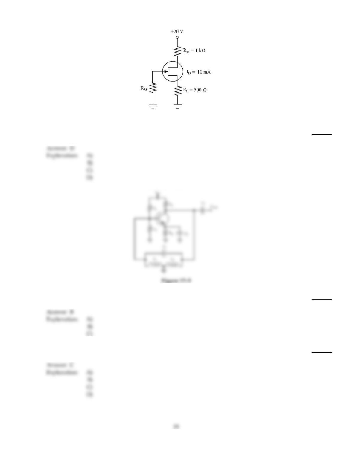
Figure 17–2
57)
Find VG in Figure 17–2.
57)
A)
10 V
B)
15 V
C)
5 V
D)
0 V
58)
The circuit in Figure 17–5 is known as a ________ oscillator because it has a ________ coil.
58)
A)
crystal, dual
B)
Hartley, dual
C)
Colpitts, dual
59)
A crystal oscillator usually has a very high ________.
59)
A)
I
B)
BW
C)
Q
D)
V
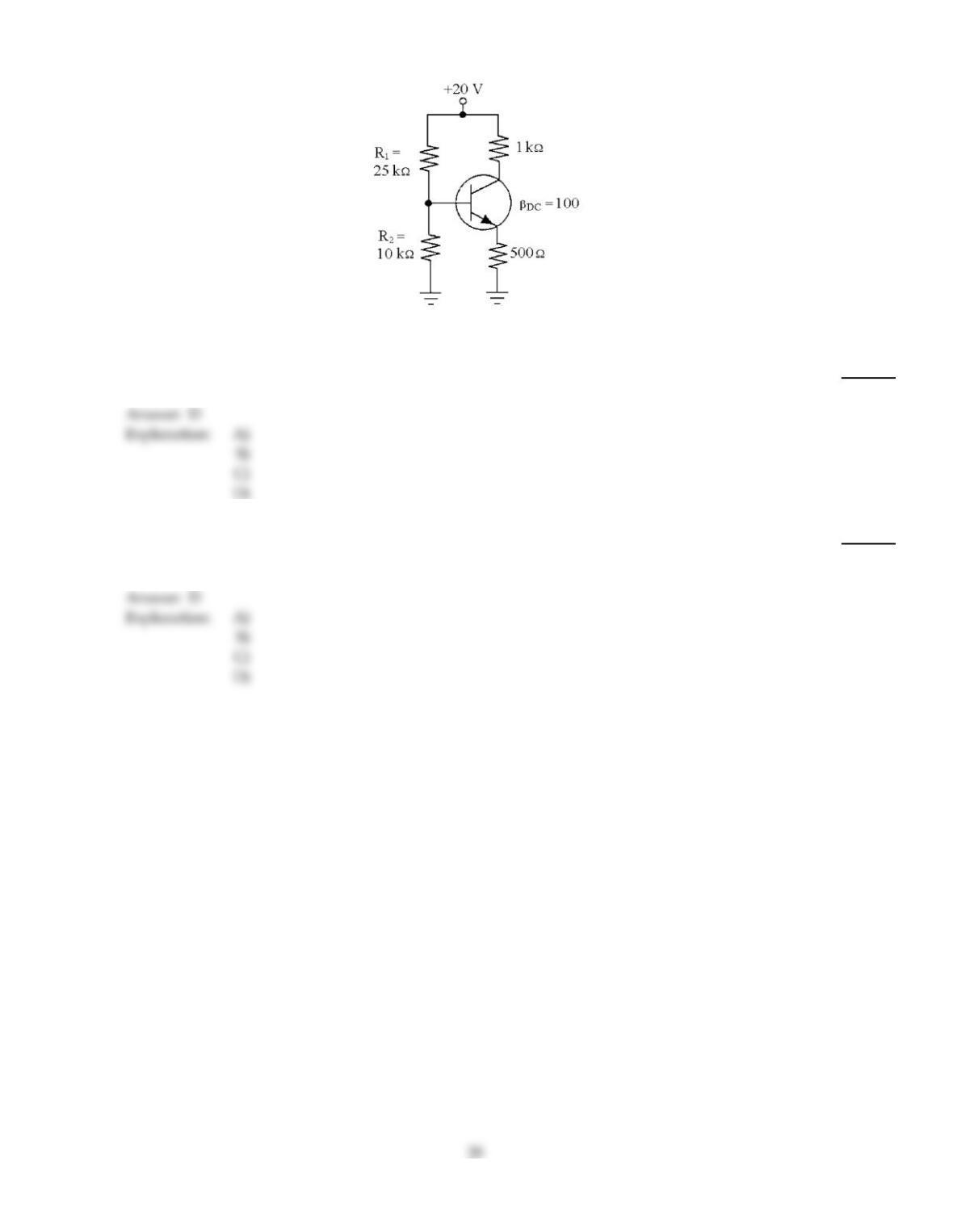
Figure 17–1
60)
Find VBE in Figure 17–1.
60)
A)
15 V
B)
5 V
C)
5.71 V
D)
0.7 V
61)
Positive feedback is defined as feeding back a portion of the output to the input such that:
61)
A)
there is no net phase shift.
B)
the two are in phase.
C)
it reinforces the signal at the input.
D)
all of these.
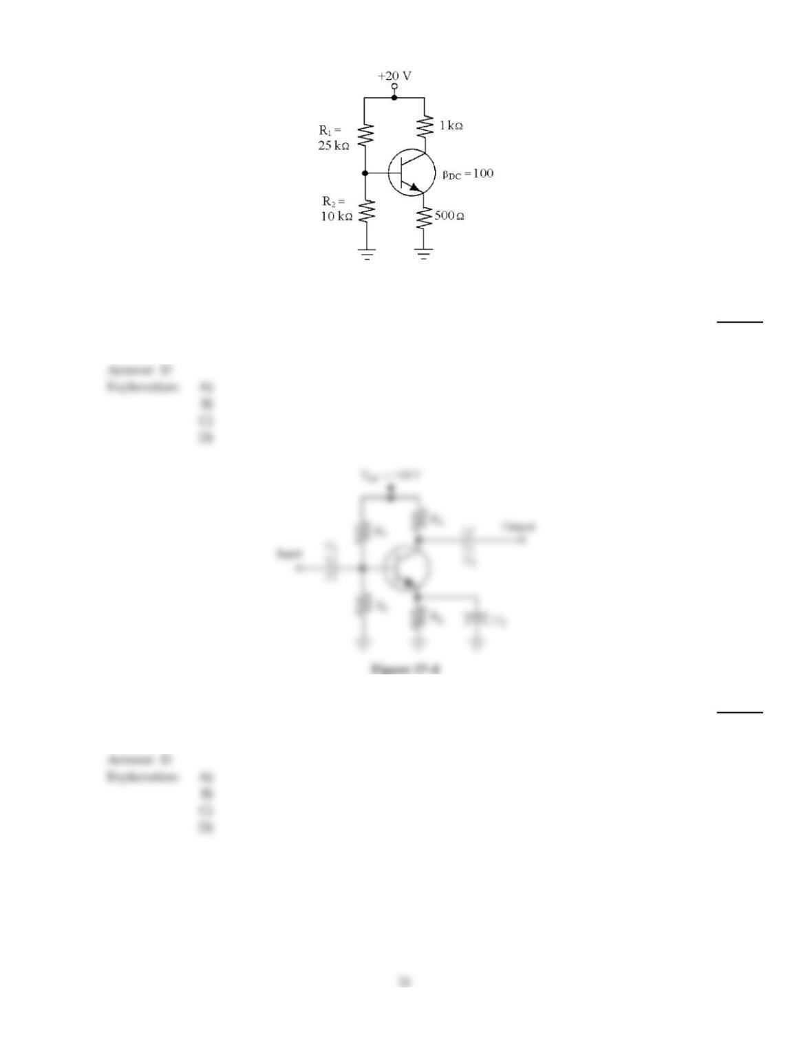
Figure 17–1
62)
If VC equals VE in Figure 17–1, the ________.
62)
A)
power is off
B)
transistor is cutoff
C)
emitter has opened
D)
emitter is shorted to the collector
63)
If the BJT’s emitter internally shorted to its collector in Figure 17–4, VCE ________.
63)
A)
decreases
B)
increases
C)
remains the same
D)
drops almost to zero
64)
The classification of transistor amplifiers by classes: A, B, C, is based on:
64)
A)
bias voltages.
B)
voltage flow.
C)
signal voltages.
D)
current flow.
65)
To analyze the operation of a BJT in an amplifier circuit, use characteristic curves of:
65)
A)
emitter current versus emitter to collector voltage.
B)
base current versus collector to emitter voltage.
C)
collector current versus collector to emitter voltage.
D)
collector current versus emitter to collector voltage.
66)
If ID= 20 mA in Figure 17–2, VG equals ________.
66)
A)
5 V
B)
0 V
C)
15 V
D)
10 V
67)
A class C amplifier conducts during ________ of the input cycle.
67)
A)
a small portion
B)
only 50%
C)
180°
D)
360°
68)
Oscillators are amplifiers that produce a repetitive waveform and that utilize:
68)
A)
degenerative feedback.
B)
negative feedback.
C)
positive feedback.
D)
both negative and positive feedback.
69)
In a class A amplifier, the output signal is ________.
69)
A)
distorted
B)
smaller in amplitude than the input
C)
clipped
D)
the same shape as the input
70)
The amplifier in Figure 17–2 uses a ________ and the gate current is ________.
70)
A)
BJT, 0 A
B)
JFET, 5 mA
C)
TRIAC, 10 mA
D)
JFET, 0 A
71)
Oscillators operate on the principle of ________.
71)
A)
attenuation
B)
positive feedback
C)
negative feedback
D)
signal feed–through
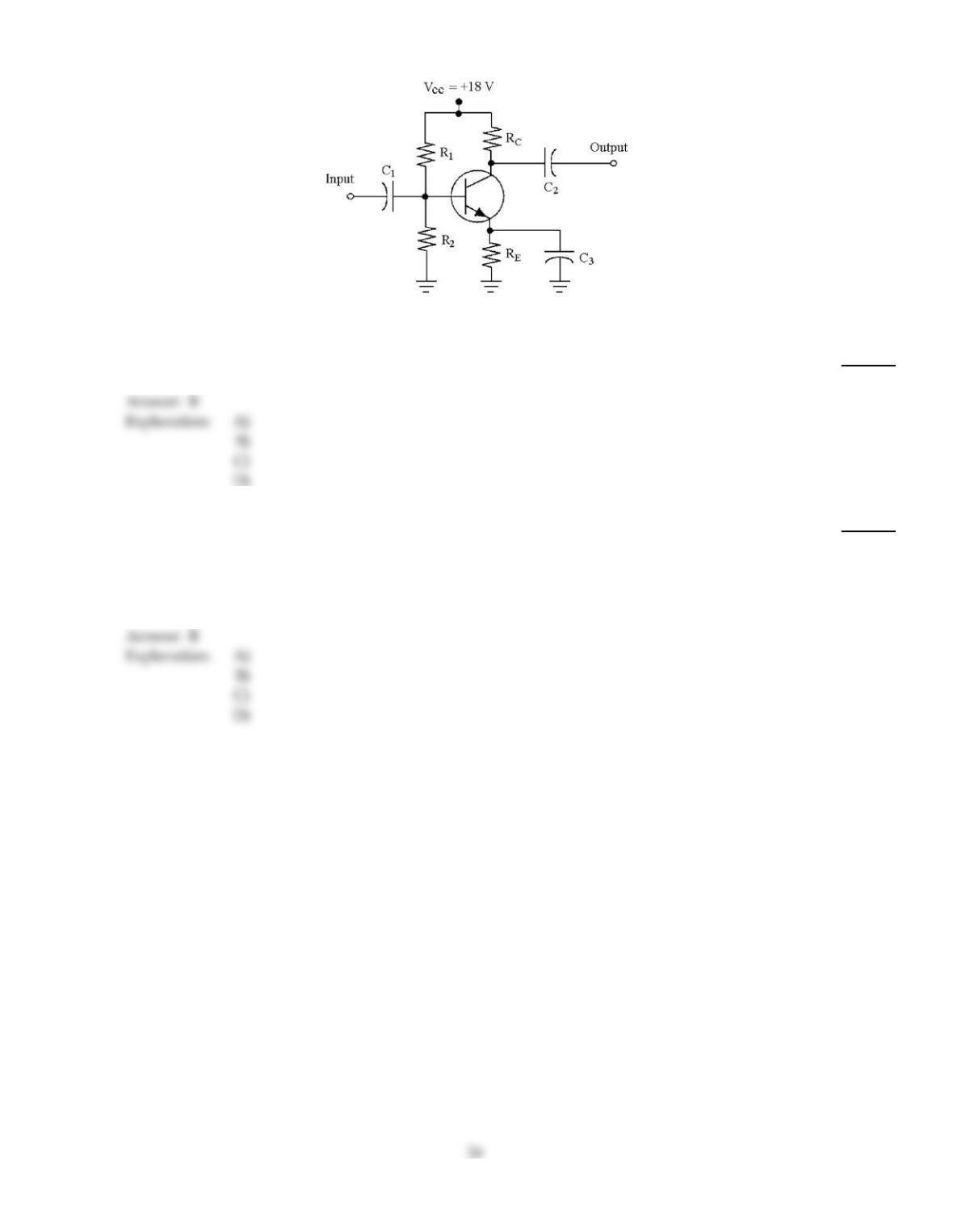
Figure 17–4
72)
Which voltage would indicate that the amplifier in Figure 17–4 is operating in cutoff?
72)
A)
VBC = 9 V
B)
VC= 18 V
C)
VCE = 9 V
D)
VBE = 7 V
73)
On transistor spec sheet, the key difference between DC and DC is that:
73)
A)
DC represents IC/IB; DC represents IB/Ic.
B)
DC represents IC/IB; DC represents IC/IE.
C)
DC represents IE/IC; DC represents IB/IC.
D)
DC represents IE/IC; DC represents IC/IE.
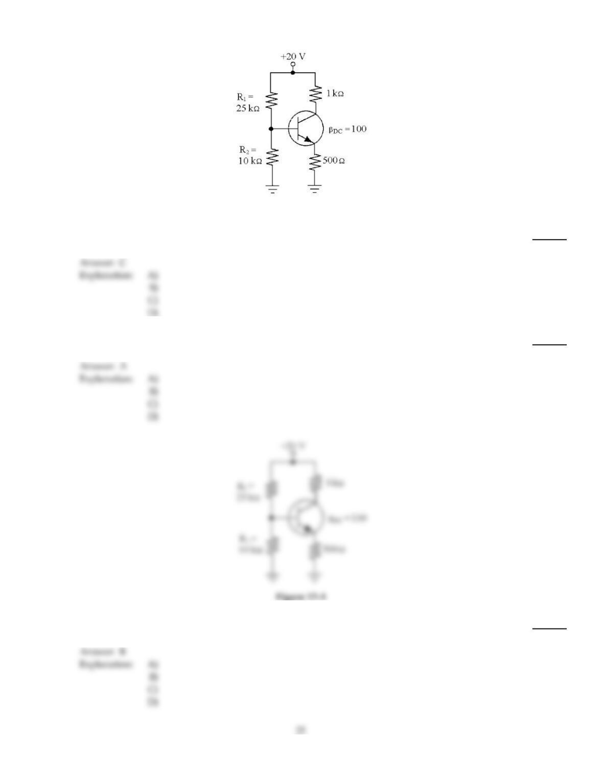
Figure 17–1
74)
If R1 opens in Figure 17–1, VC equals ________.
74)
A)
0 V
B)
10 V
C)
20 V
D)
0.7 V
75)
The most accurate signal reproduction in transistor amplifiers is provided by:
75)
A)
class A
B)
class B
C)
class C
D)
class AB
Figure 17–1
76)
Find VCE in Figure 17–1.
76)
A)
16.4 V
B)
7.10 V
C)
11.4 V
D)
6.4 V
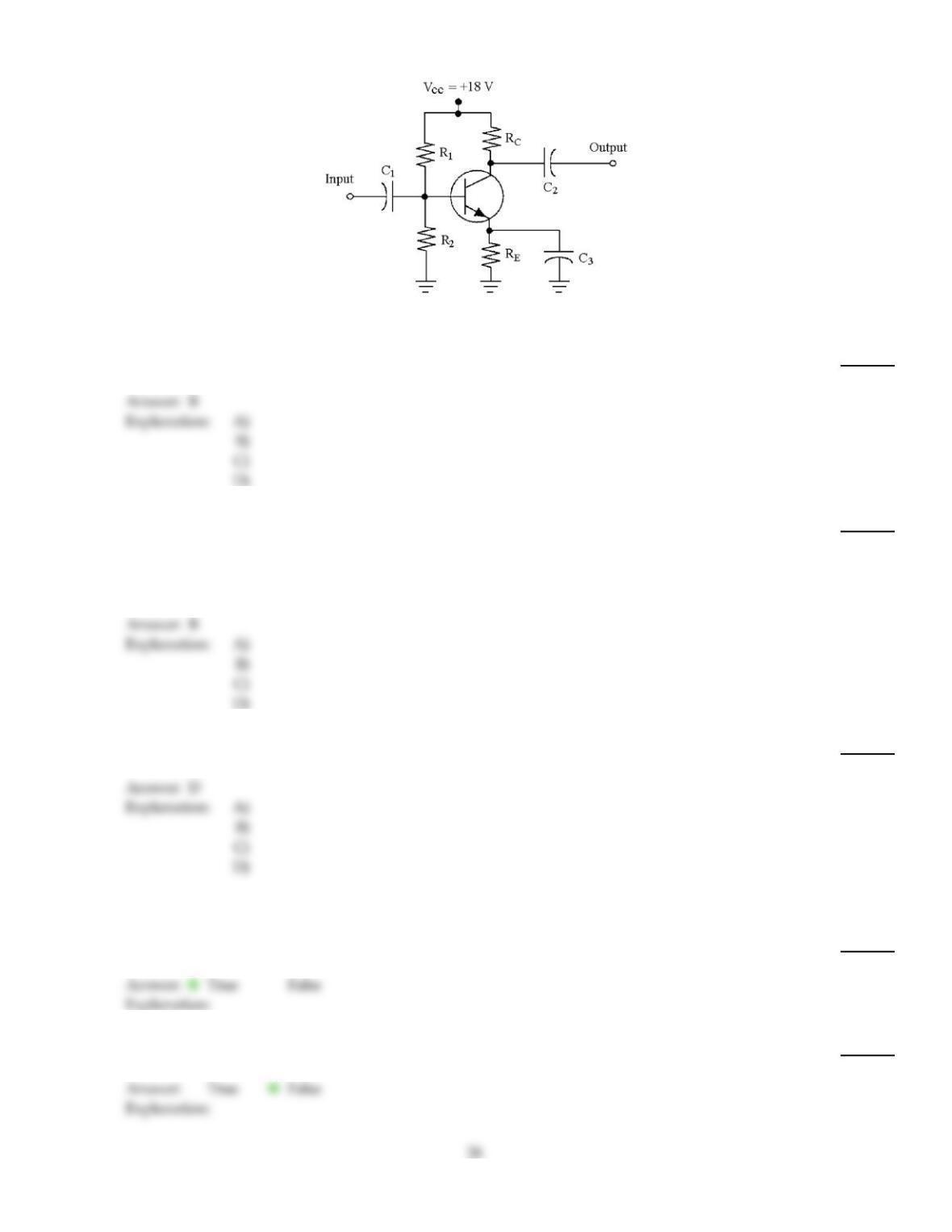
Figure 17–4
77)
Which voltage might allow the circuit in Figure 17–4 to operate with minimum distortion?
77)
A)
VCE = 0.15 V
B)
VBE = 0.7 V
C)
VBC = 0 V
D)
VC= 18 V
78)
If the base current increases, ________.
78)
A)
the collector current increases and the emitter current decreases
B)
the collector current increases and the emitter current increases
C)
the collector current increases and the emitter current does not change
D)
the collector current decreases and the emitter current decreases
79)
A Class ________ amplifier is very efficient. It is useful mainly at ________ frequencies.
79)
A)
C, audio
B)
B, audio
C)
A, radio
D)
C, radio
TRUE/FALSE. Write ‘T’ if the statement is true and ‘F’ if the statement is false.
80)
A common–collector amplifier has a high input impedance compared to a common–emitter
amplifier.
80)
81)
The general characteristics of a common–emitter amplifier are high voltage gain, high current gain
and no phase reversal between the input and output voltages.
81)

82)
To correctly bias a BJT, reverse–bias the base–emitter junction and forward–bias the base–collector
junction.
82)
83)
An amplifier that provides its own input is called an oscillator.
83)
84)
The gate current in a JFET is normally zero.
84)
85)
The general characteristics of a common–emitter amplifier are low voltage gain, low current gain
and very high power gain.
85)
86)
An N–channel JFET has three elements: source, gate, and drain.
86)
87)
Two types of FETs are the JFET and the MOSFET.
87)
88)
A depletion–type MOSFET can operate with a positive or negative value of VGS.
88)
89)
A current gain of almost one is a characteristic of a common–base amplifier.
89)
90)
A BJT has three elements: emitter, gate, and collector.
90)
91)
An enhancement–type MOSFET can operate with a positive value of VGS.
91)
92)
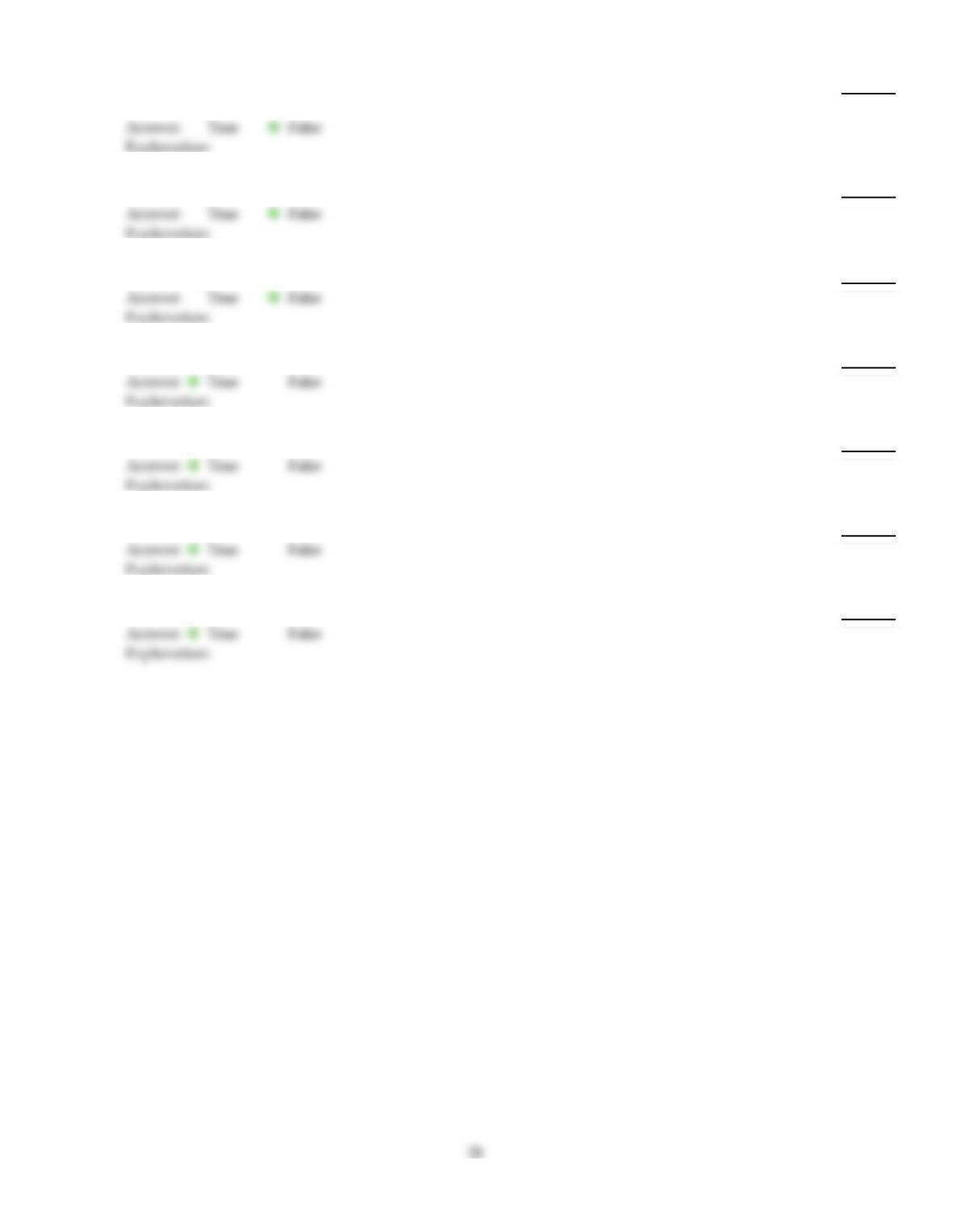
If a common–emitter amplifier measures the same voltage on the collector as VCC, the amplifier is
operating in saturation.
92)
93)
The voltage gain of several amplifiers in series is found by adding the individual stage voltage
gains.
93)
94)
Voltage gain can be found by AV=VIN ÷VOUT
94)
95)
The two types of BJTs are the PNP and the P–channel.
95)
96)
Class C amplifiers are used primarily at radio frequencies.
96)
97)
The two types of BJTs are the NPN and PNP.
97)
98)
A transistor can be used as an electronic switch.
98)
99)
The overall voltage gain of a multistage amplifier is the product of the individual stage gains.
99)

Answer Key
Testname: C17

Answer Key
Testname: C17
30