Exam
Name___________________________________
MULTIPLE CHOICE. Choose the one alternative that best completes the statement or answers the question.
1)
When a BJT amplifier is saturated, VCE is about ________ and IC is ________.
1)
A)
25 V, 10 mA
B)
zero, minimum
C)
VCC, minimum
D)
zero, maximum
2)
Which voltage might indicate that the amplifier in Figure 17–1 is cut off?
2)
A)
VBE = 0.7 V
B)
VCE = 0 V
C)
VE= 20 V
D)
VC= 20 V
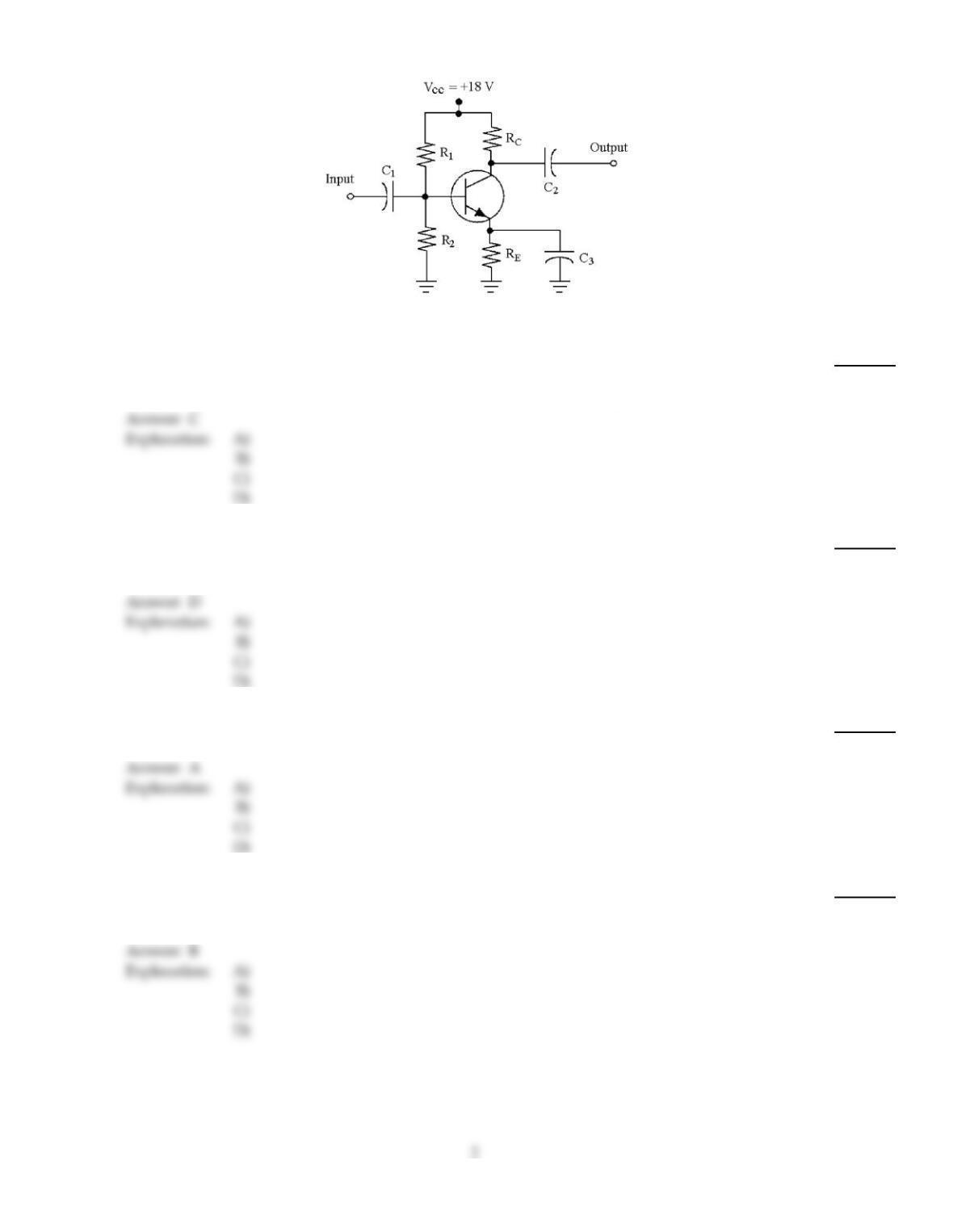
Figure 17–4
3)
If the collector opens in Figure 17–4, the output voltage ________.
3)
A)
increases
B)
remains the same
C)
decreases to zero
D)
varies with temperature
4)
Amplifiers are electronic circuits that accept an AC input signal and produce an output signal that
represents a:
4)
A)
power gain.
B)
voltage gain.
C)
current gain.
D)
all of these.
5)
If a transistor’s beta equals 30 and IB equals 1 mA, IC equals ________.
5)
A)
30 mA
B)
1 mA
C)
0.33 mA
D)
unknown
6)
Which one of these amplifiers has a very high power gain?
6)
A)
common–collector
B)
common–emitter
C)
common–reference
D)
common–gate
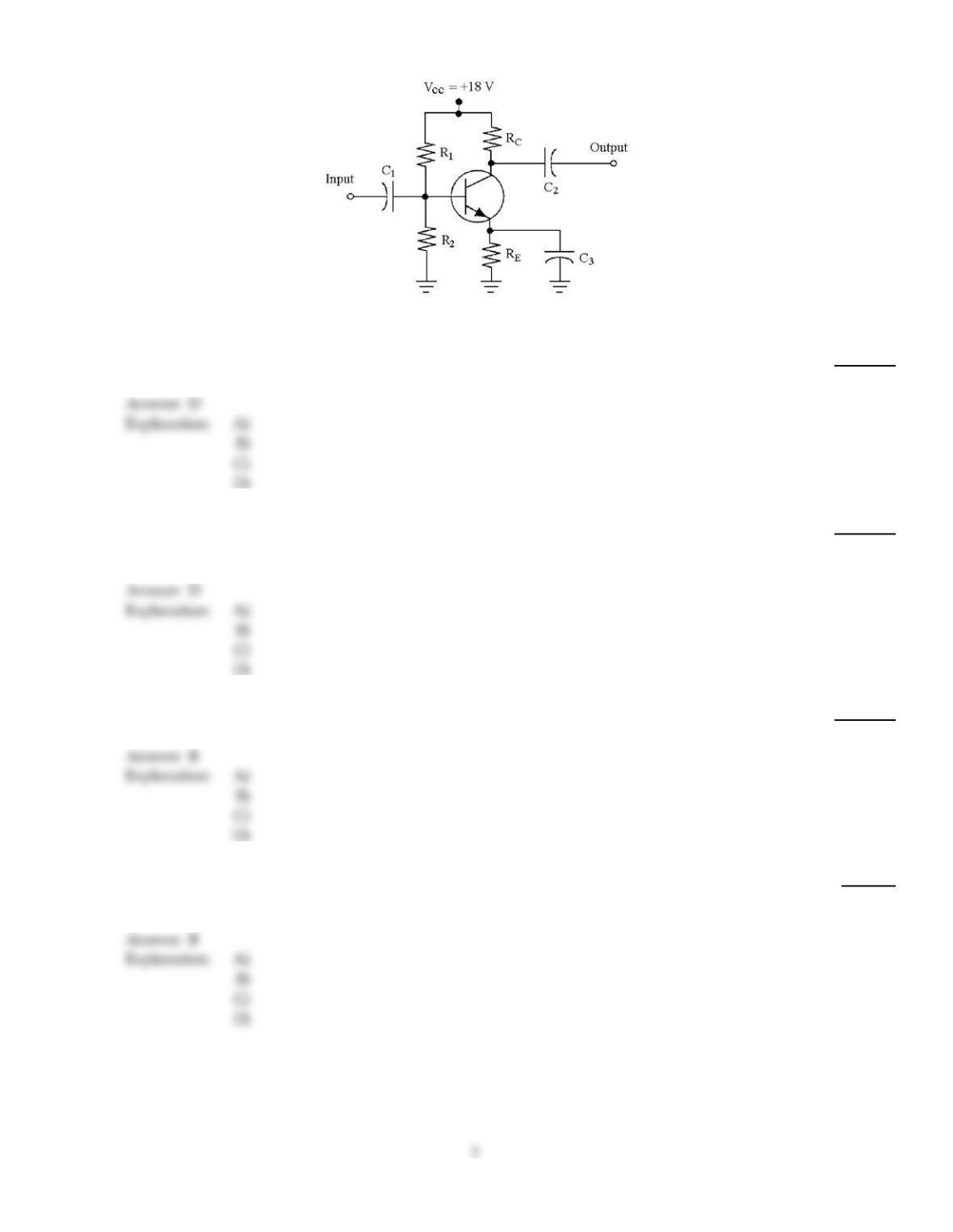
Figure 17–4
7)
If R1 opens in Figure 17–4, VC equals ________.
7)
A)
0 V
B)
VE
C)
9 V
D)
18 V
8)
If RE opens in Figure 17–4, VE ________.
8)
A)
drops almost to zero
B)
decreases
C)
remains the same
D)
increases
9)
Which voltage would enable the circuit in Figure 17–4 to operate with little distortion?
9)
A)
VBE = 7 V
B)
VCE = 9 V
C)
VC= 18 V
D)
VBC = 0 V
10)
A crystal oscillator uses a crystal to determine the ________.
10)
A)
dc output
B)
output frequency
C)
amount of positive feedback
D)
amount of negative feedback
11)
One advantage of the Darlington pair is ________.
11)
A)
decreasing the input impedance
B)
less cost
C)
increased overall beta
D)
increased overall voltage gain
12)
The Class B amplifier conducts for ________ of the input cycle.
12)
A)
only 10°
B)
180°
C)
a small portion
D)
360°
B
13)
If C3 opens in Figure 17–4, ________.
13)
A)
the dc emitter voltage decreases
B)
the dc emitter voltage increases
C)
the voltage gain increases
D)
the voltage gain decreases
D
C
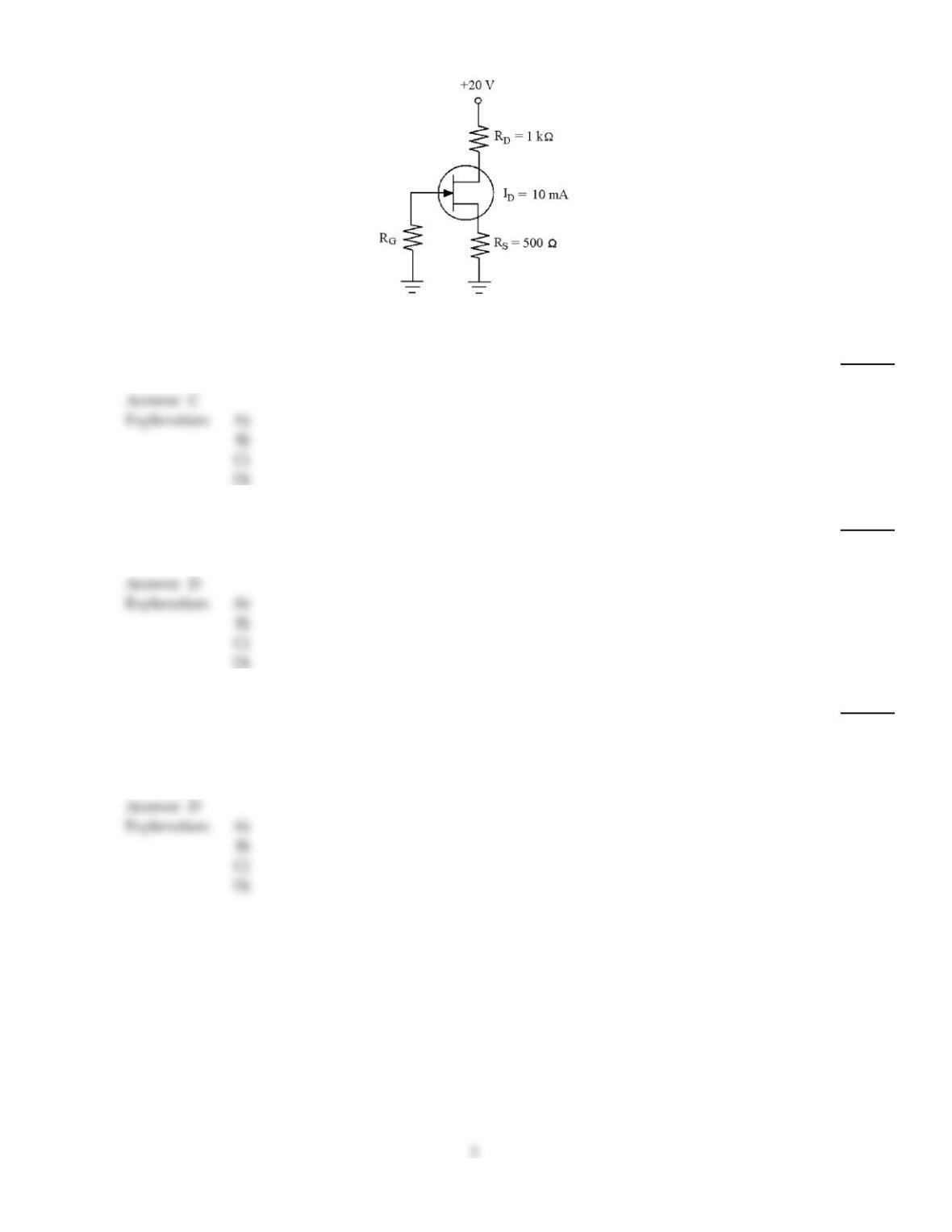
Figure 17–2
14)
If ID= 15 mA in Figure 17–2, VGS equals ________.
14)
A)
25 V
B)
0 V
C)
–7.5 V
D)
15 V
15)
When a negative gate–to–source voltage is applied to an N–channel MOSFET, it operates ________.
15)
A)
in the cutoff state
B)
in the enhancement mode
C)
in the saturated state
D)
in the depletion mode
16)
The terms common–emitter and common–collector mean that:
16)
A)
one of the leads is a common input signal point.
B)
one of the leads is a common reference to the other two leads.
C)
one of the leads is a common DC bias point.
D)
all of these.
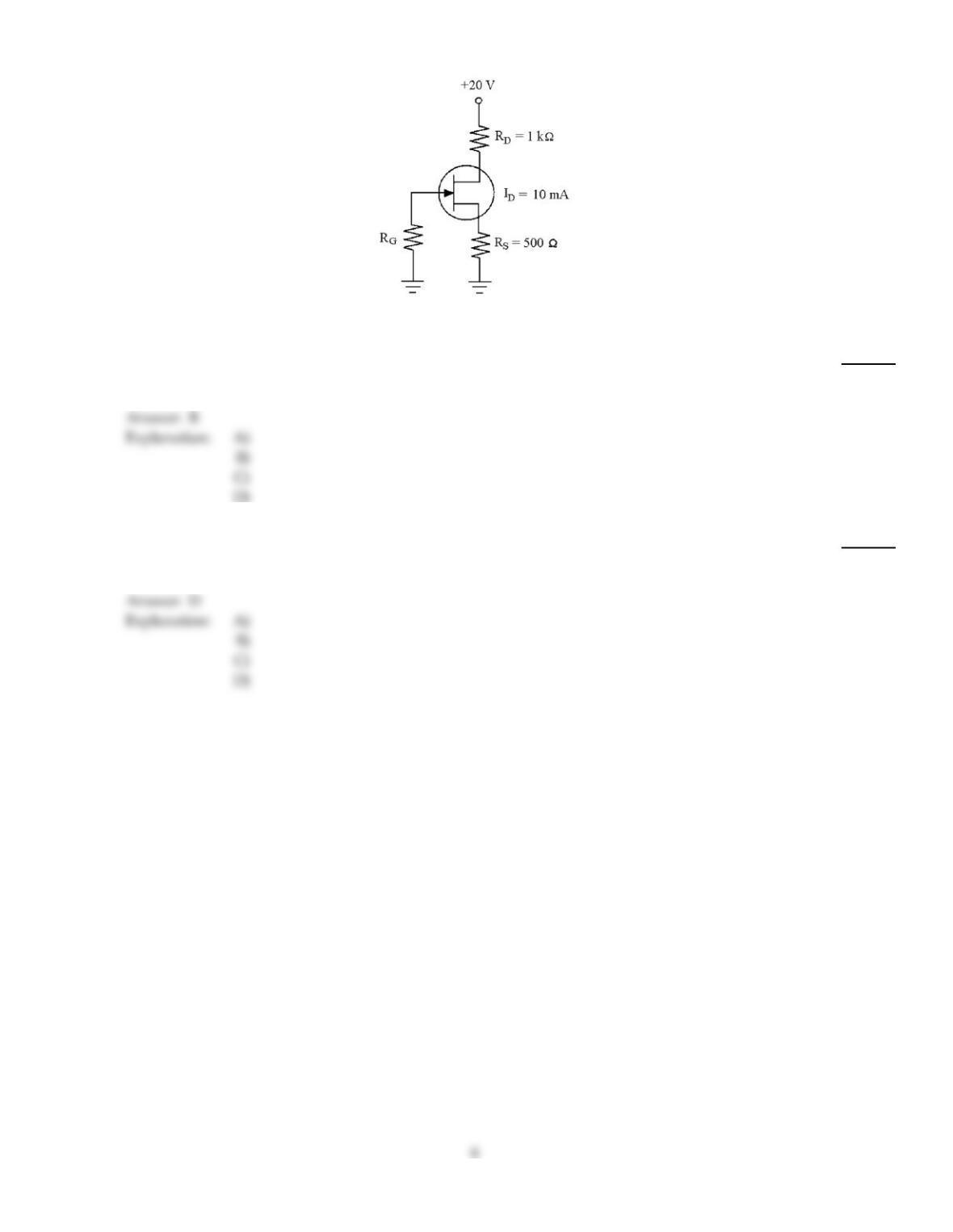
Figure 17–2
17)
The device in Figure 17–2 is a ________.
17)
A)
NPN type BJT
B)
N–channel JFET
C)
P–channel MOSFET
D)
depletion type MOSFET
18)
Which one of these amplifiers has high input resistance and low output resistance?
18)
A)
common–cause
B)
common–current
C)
common–emitter
D)
common–collector
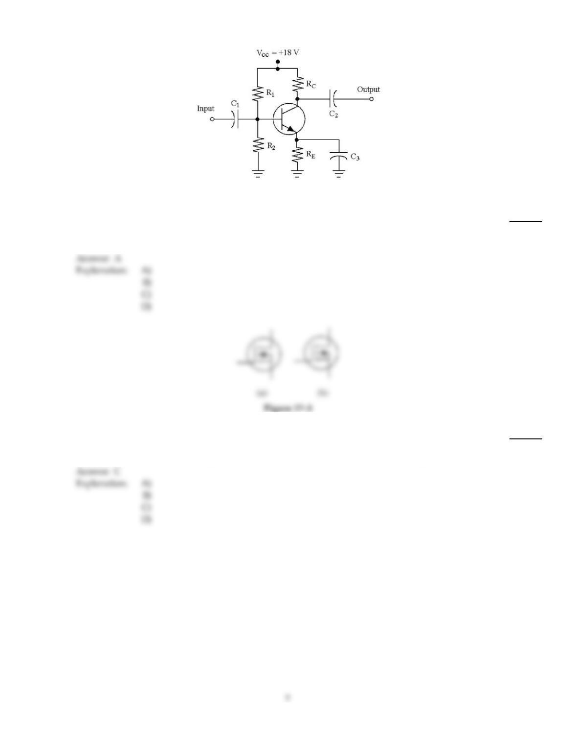
Figure 17–4
19)
If R1 shorts in Figure 17–4, VC ________.
19)
A)
decreases to VE
B)
decreases to 0 V
C)
increases to VCC
D)
does not change
20)
The symbol in Figure 17–3(b) represents the ________.
20)
A)
N–channel enhancement–type MOSFET
B)
N–channel depletion–type JFET
C)
P–channel enhancement–type MOSFET
D)
N–channel enhancement–type JFET
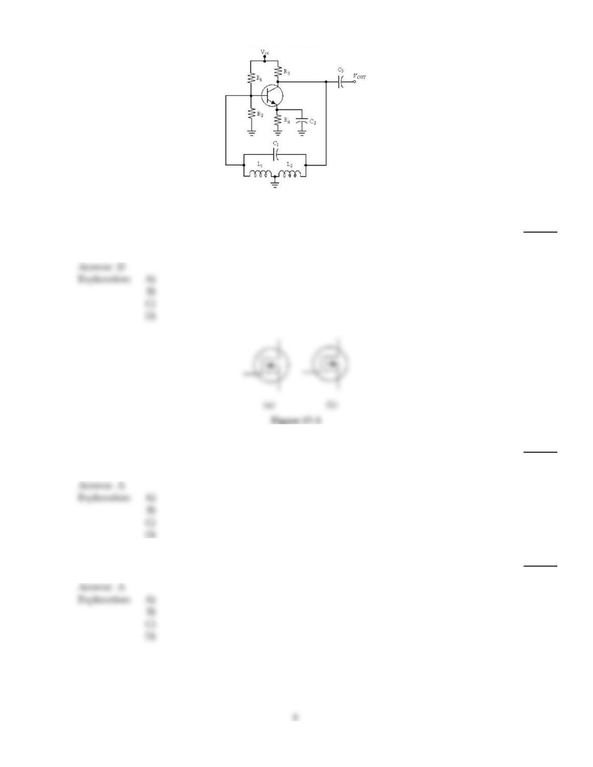
Figure 17–5
21)
In Figure 17–5, L1, L2 and C1 form a ________ that provides ________ feedback to the amplifier.
21)
A)
tank circuit, out–of–phase
B)
feedback network, negative
C)
tank circuit, negative
D)
tank circuit, positive
22)
The symbol in Figure 17–3(a) represents the ________.
22)
A)
N–channel enhancement–type MOSFET
B)
N–channel enhancement–type JFET
C)
P–channel enhancement–type MOSFET
D)
N–channel depletion–type JFET
23)
The largest theoretical voltage gain obtainable with a CC amplifier is ________.
23)
A)
1
B)
100
C)
10
D)
dependent on
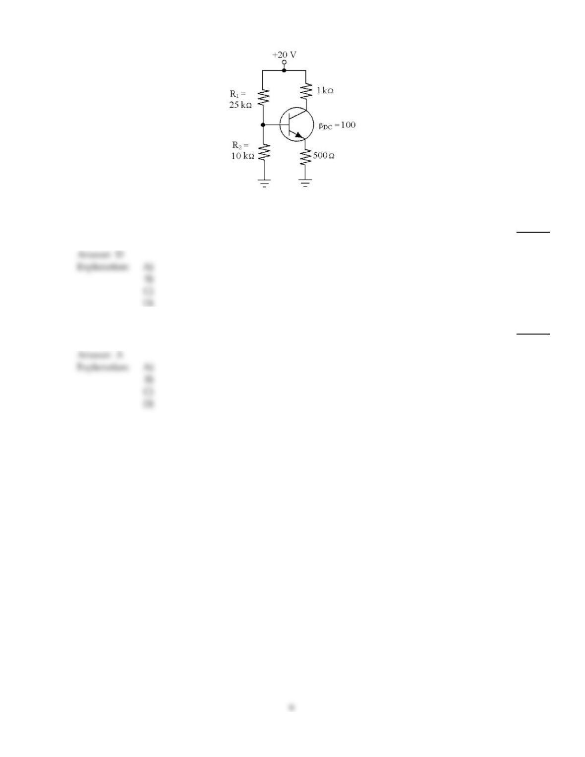
Figure 17–1
24)
If the emitter resistor opened in Figure 17–1, VB equals ________.
24)
A)
0.7 V
B)
20 V
C)
0 V
D)
5.71 V
25)
What is the total voltage gain of a three–stage amplifier that has stage gains of 22, 112, and 8?
25)
A)
19,712
B)
1,420
C)
197,120
D)
142
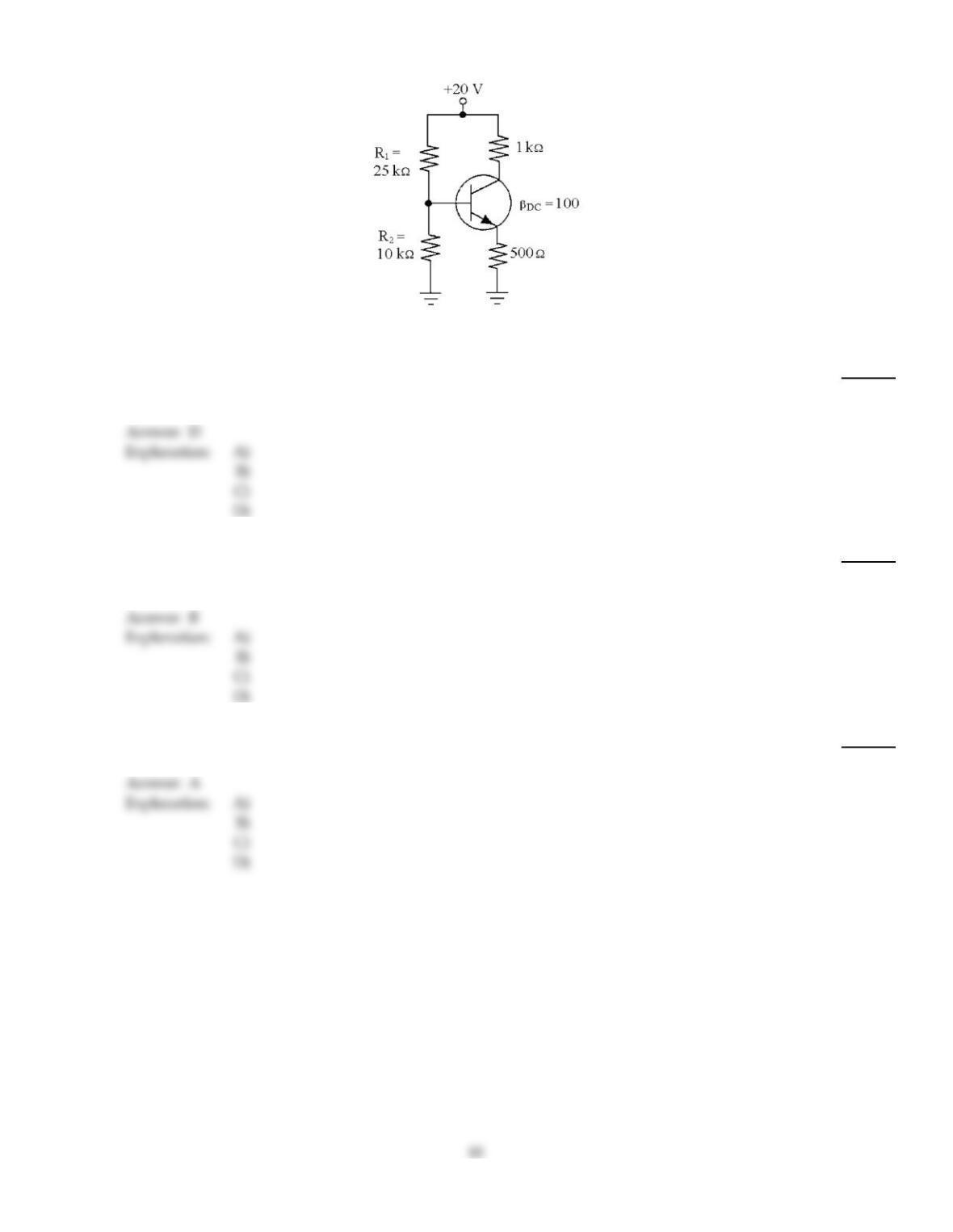
Figure 17–1
26)
If the collector–to–emitter voltage is about 0 V in Figure 17–1, the possible trouble is ________.
26)
A)
this is a normal condition
B)
the transistor is open
C)
the amplifier is cut off
D)
the amplifier is saturated
27)
If R2 opens in Figure 17–1, IC ________.
27)
A)
remains the same
B)
increases
C)
decreases
D)
decreases to zero
28)
If VCC equals 15 V in Figure 17–1, VBE equals ________.
28)
A)
0.7 V
B)
5 V
C)
15 V
D)
4.71 V
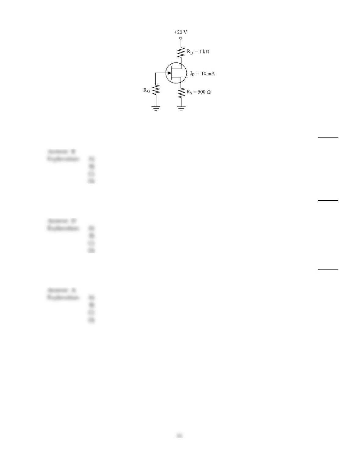
Figure 17–2
29)
The amplifier in circuit Figure 17–2 uses a ________ and VD equals ________.
29)
A)
JFET, 0 V
B)
JFET, 10 V
C)
BJT, 10 V
D)
TRIAC, 5 V
30)
In using BJT characteristic curves, the straight line drawn between the cutoff and the saturation
points is called:
30)
A)
saturation line.
B)
operating line.
C)
cutoff line.
D)
load line.
31)
Which one of these amplifiers does NOT have the output in phase with the input?
31)
A)
common–source
B)
common–collector
C)
common–drain
D)
common–law
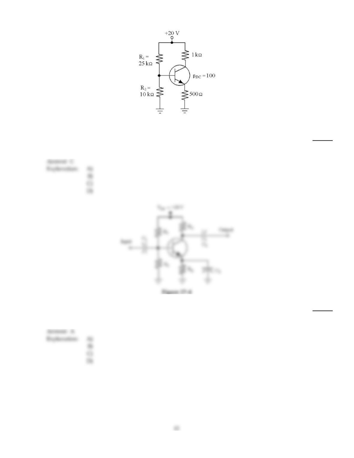
Figure 17–1
32)
If VC= 20 V in Figure 17–1, which statement describes a possible trouble?
32)
A)
The amplifier is saturated.
B)
The power is off.
C)
The amplifier is cut off.
D)
This is normal.
33)
If the BJT’s collector opens internally in Figure 17–4, VB ________.
33)
A)
remains the same
B)
increases
C)
decreases
D)
drops almost to zero

34)
In all N–channel FET’s, the current into the source equals the current leaving the ________.
34)
A)
drain
B)
source
C)
collector
D)
emitter
35)
To recognize transistor packages and identify the terminals, look for:
35)
A)
the flat side.
B)
the protruding tab.
C)
the imprinted dot.
D)
all of these.
36)
Which of the following amplifiers has phase inversion?
36)
A)
common–collector
B)
common–crystal
C)
common–drain
D)
common–emitter
37)
The most popular and widely used transistor amplifier configuration is the:
37)
A)
common–collector.
B)
common–purpose.
C)
common–drain.
D)
common–emitter.
38)
In using BJT characteristic curves, the intersection of the load line with a specific base current curve
is called:
38)
A)
intersection point.
B)
base point.
C)
Q point.
D)
nudpoint.
39)
Although BJT transistors are current operated devices, a key characteristic is the signal voltage gain
as an amplifier specified as:
39)
A)
Av
RB/RE.
B)
Av
RC/RB.
C)
Av
RC/RE.
D)
Av
RE/RC.
40)
Beta () is the ratio of ________.
40)
A)
output voltage to input voltage
B)
emitter current to base current
C)
collector current to base current
D)
collector current to emitter current
C
41)
The circuit in Figure 17–5 is a ________ oscillator and uses ________ feedback.
41)
A)
Colpitts, negative
B)
Hartley, positive
C)
Colpitts, positive
D)
crystal, negative
B
42)
What is the total voltage gain of a three–stage amplifier that has stage gains of 17, 142, and 4?
42)
A)
28,968
B)
2414
C)
163
D)
9656
D
C
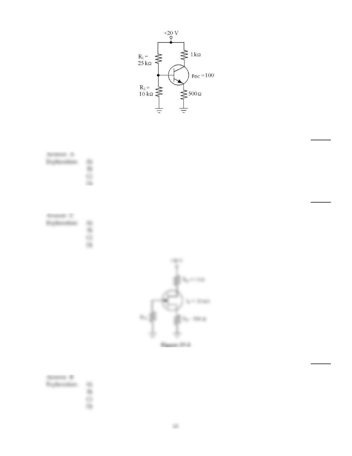
Figure 17–1
43)
If the BJT‘s collector opened internally in Figure 17–1, VRC equals ________.
43)
A)
0 V
B)
10 V
C)
VBE
D)
20 V
44)
If the base–emitter junction opened in Figure 17–1, VE equals ________.
44)
A)
10 V
B)
20 V
C)
0 V
D)
5 V
45)
Find VGS in Figure 17–2.
45)
A)
10 V
B)
–5 V
C)
–10 V
D)
5 V