Exam
Name___________________________________
MULTIPLE CHOICE. Choose the one alternative that best completes the statement or answers the question.
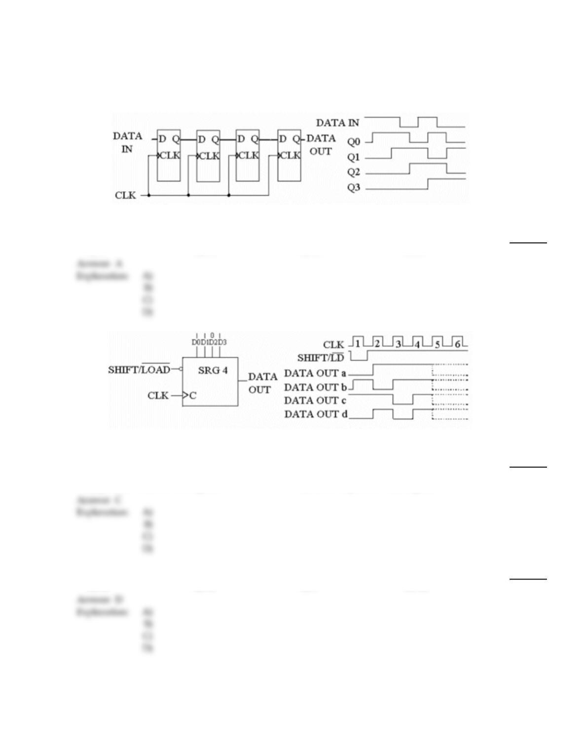
Figure 8–1
1)
How many clock cycles are required to enter a data group into the register in Figure 8–1?
1)
A)
4
B)
32
C)
16
D)
2
Figure 8–3
2)
The circuit shown in Figure 8–3 is a ________.
2)
A)
demultiplexer
B)
multiplexer
C)
parallel–in serial–out register
D)
serial–in parallel–load register
C
3)
What is the modulus of a 6–stage Johnson counter?
3)
A)
64
B)
32
C)
6
D)
12
D
1
A
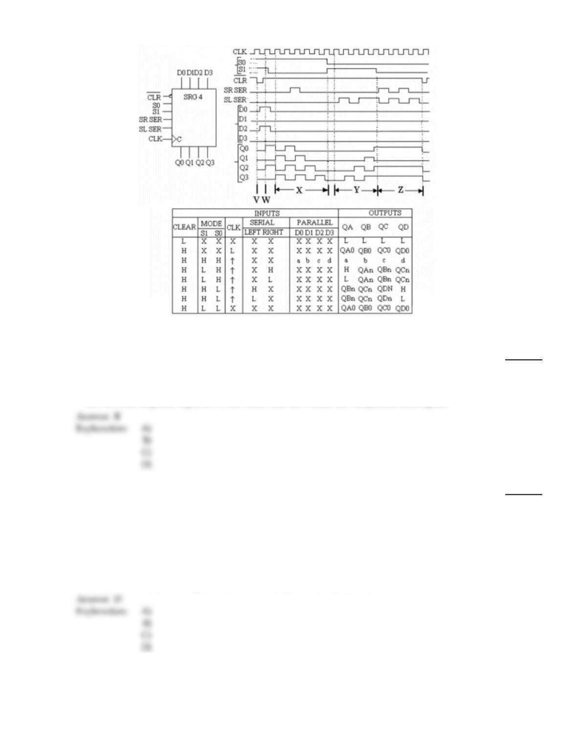
Figure 8–5
4)
Refer to the Function Table in Figure 8–5. What occurs if the CLEAR, S1 and S0 inputs all go HIGH?
4)
A)
The operation of the register is inhibited.
B)
The parallel data inputs are loaded and passed to the parallel data outputs.
C)
The parallel registers are RESET and the serial data inputs are inhibited.
D)
The exact response depends on the values that are loaded into the parallel data inputs.
5)
A technician is testing an undocumented digital system with a signature analyzer. What indications
should the technician look for?
5)
A)
Look for similar signatures that show up at different points in the circuit; no two points
should be the same.
B)
As signals flow from one circuit to another, changes will take place; look for changes in the
signatures, especially between inputs and outputs.
C)
Use a logic analyzer to verify the correct operation of the signature analyzer; once its accuracy
has been confirmed, its indications can be relied upon for troubleshooting.
D)
Without documented signatures, the instrument is basically useless.
2
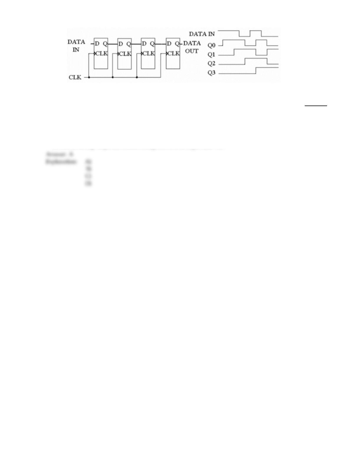
Figure 8–1
6)
The circuit in Figure 8–1 fails to produce the proper data output. The individual flip–flops are
checked with a logic probe and pulser and each checks OK. What is the most likely cause of the
problem?
6)
A)
One of the clock input lines is open.
B)
The data output line is grounded.
C)
One of the interconnect lines between two stages has a solder bridge to ground.
D)
One of the flip–flops has a solder bridge between its input and Vcc.
3
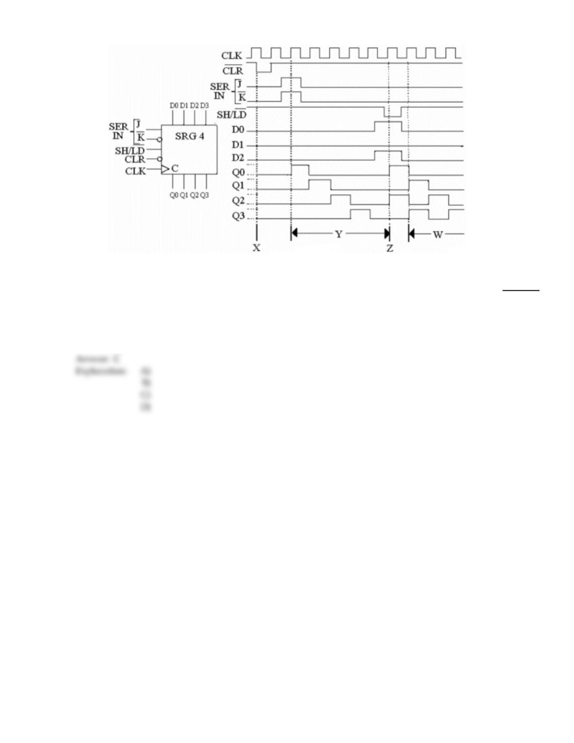
Figure 8–4
7)
Refer to Figure 8–4. What occurs at point ‘X’ on the timing diagram?
7)
A)
The inputs will be disabled.
B)
All inputs and outputs will be reset to LOW.
C)
The outputs will all go LOW.
D)
Only the CLK will be disabled during this time, preventing any transfer of data between
inputs and outputs.
4
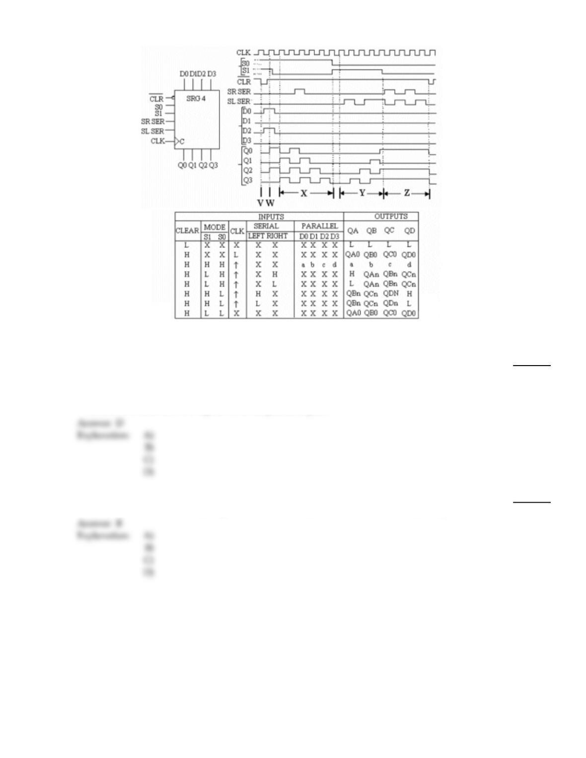
Figure 8–5
8)
Refer to Figure 8–5. What occurs at point ‘W’ on the timing diagram?
8)
A)
The parallel inputs are inhibited prevented from loading into the register.
B)
The outputs are cleared set to LOW.
C)
The serial inputs are loaded into the register.
D)
Data is loaded into the register from the parallel inputs.
9)
Which of the following is a shift register counter?
9)
A)
Decade
B)
Ring
C)
BCD
D)
Binary
5
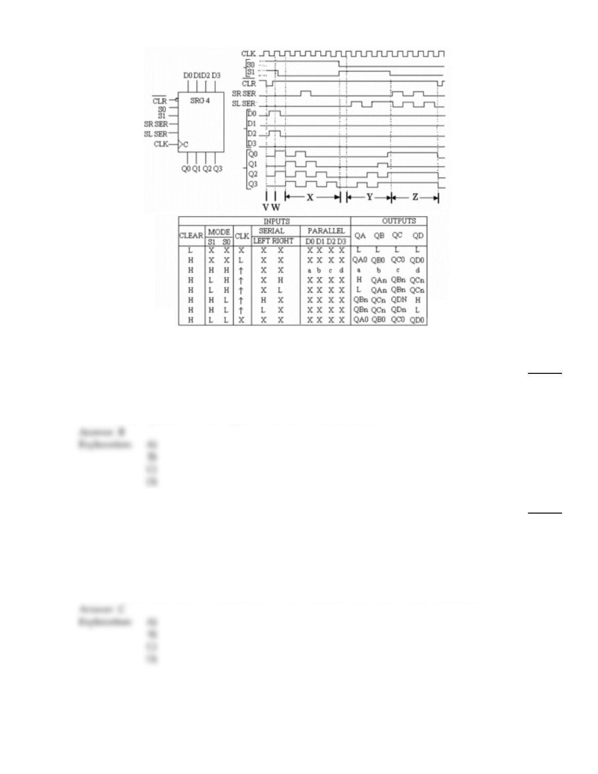
Figure 8–5
10)
What type of device is shown in Figure 8–5?
10)
A)
2–bit serial–in 4–bit parallel–out bidirectional shift register.
B)
4–bit bidirectional universal shift register.
C)
2–way parallel–in serial–out bidirectional register.
D)
Parallel–in parallel–out shift register with bidirectional data flow.
11)
What does UART stand for, and what does it do?
11)
A)
Universal ASCII Relay Transmission; defines a method (standard) by which data
communications can be made between parallel and serial devices or systems.
B)
United Artists Radio and Television; the standard data interfacing system first used by the
movie industry.
C)
Universal Asynchronous Receiver Transmitter; it is used to interface the parallel data bus in a
typical computer system to serial data transmission lines.
D)
Universal ASCII Receiver Transmitter; it is used to transmit and receive ASCII characters.
6
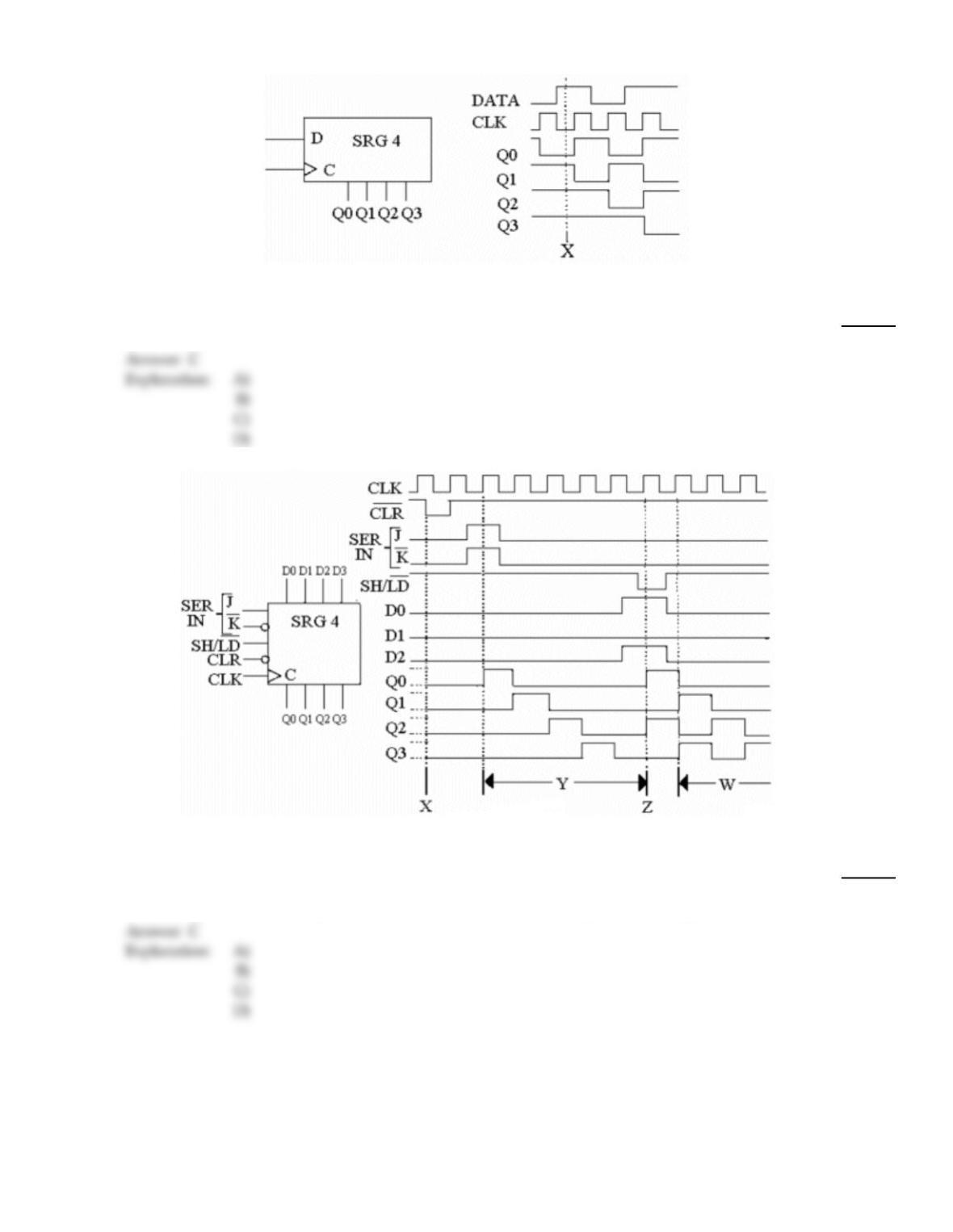
Figure 8–2
12)
Refer to the circuit and waveforms in Figure 8–2. What value is stored in the register at time ‘X’?
12)
A)
0 1 1 1
B)
0 1 0 1
C)
1 1 1 0
D)
0 1 1 0
Figure 8–4
13)
What type of register is shown in Figure 8–4?
13)
A)
Serial–in parallel–out register
B)
Serial/parallel–in parallel–out register
C)
Parallel–access shift register
D)
Parallel–in parallel–out register
Explanation:
7
Explanation:
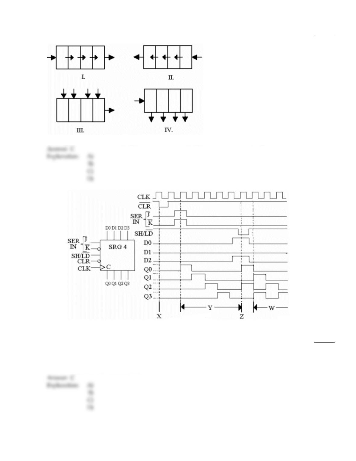
14)
Which of the illustrations below represents the function of a parallel–in serial–out register?
14)
A)
Figure I.
B)
Figure II.
C)
Figure III.
D)
Figure IV.
Figure 8–4
15)
Refer to Figure 8–4. What occurs during the time interval labeled ‘Y’?
15)
A)
Clock pulses are toggled through the register.
B)
Parallel data is shifted through the register.
C)
Serial data is shifted through the register.
D)
Parallel data transfer takes place.
8
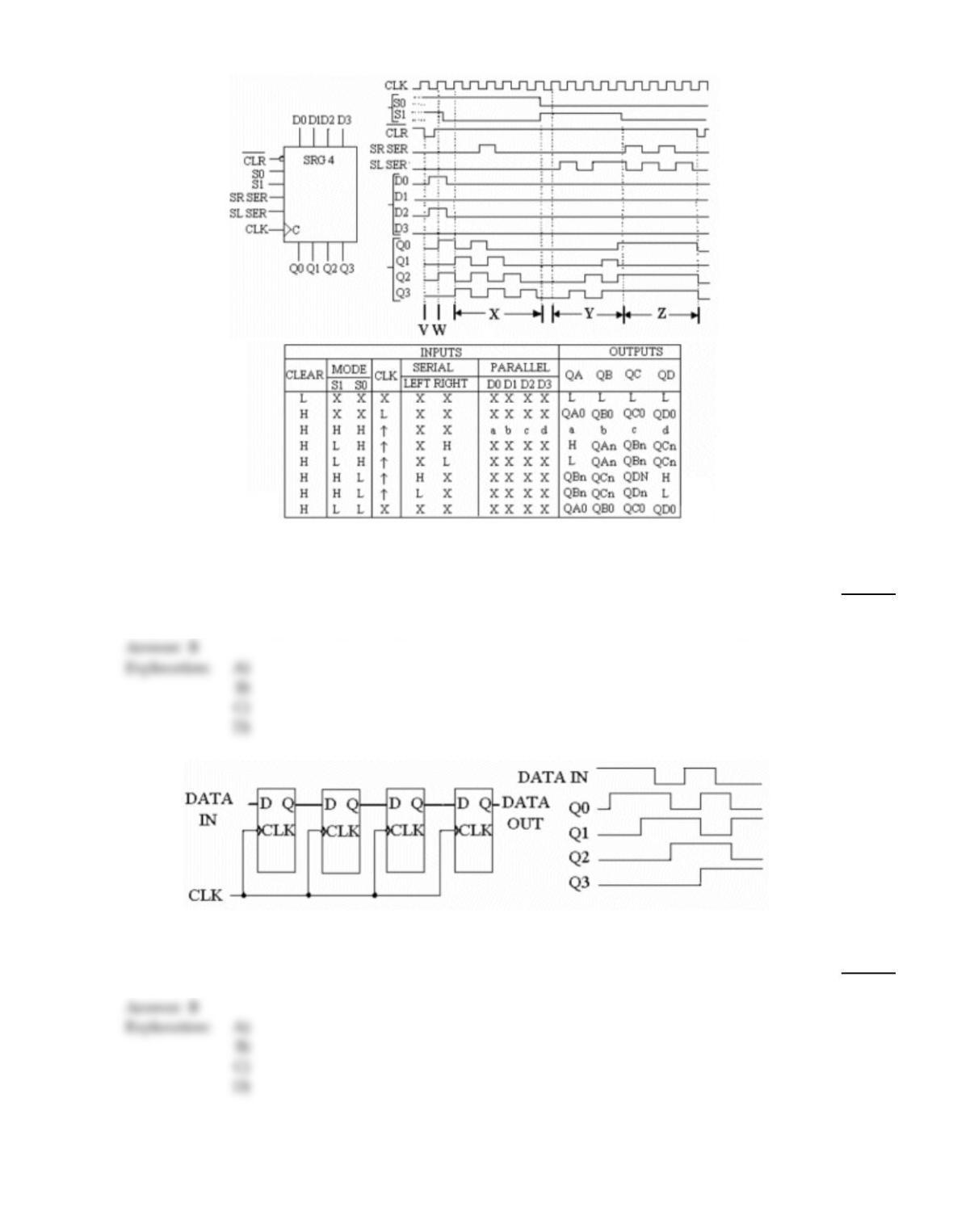
Figure 8–5
16)
Refer to Figure 8–5. What occurs during the interval labeled ‘Y’ on the timing diagram?
16)
A)
Serial data is entered into the register.
B)
Data is shifted left through the register.
C)
Data is shifted right through the register.
D)
Parallel data is entered into the register.
Figure 8–1
17)
How many data bits can be stored in the register shown in Figure 8–1?
17)
A)
16
B)
4
C)
2
D)
32
9
18)
What is the primary function of a register?
18)
A)
Data storage (memory)
B)
Encoding
C)
Decoding
D)
Counting
19)
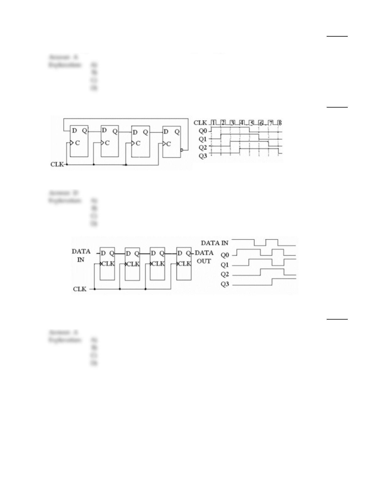
The circuit shown below is a ________.
19)
A)
BCD counter
B)
decade counter
C)
ring counter
D)
Johnson counter
Explanation:
Figure 8–1
20)
After the DATA IN waveform in Figure 8–1 is complete, what value is stored in the register?
20)
A)
1 1 0 1
B)
1 0 1 0
C)
0 1 0 1
D)
1 0 0 1
Explanation:
10
Explanation:
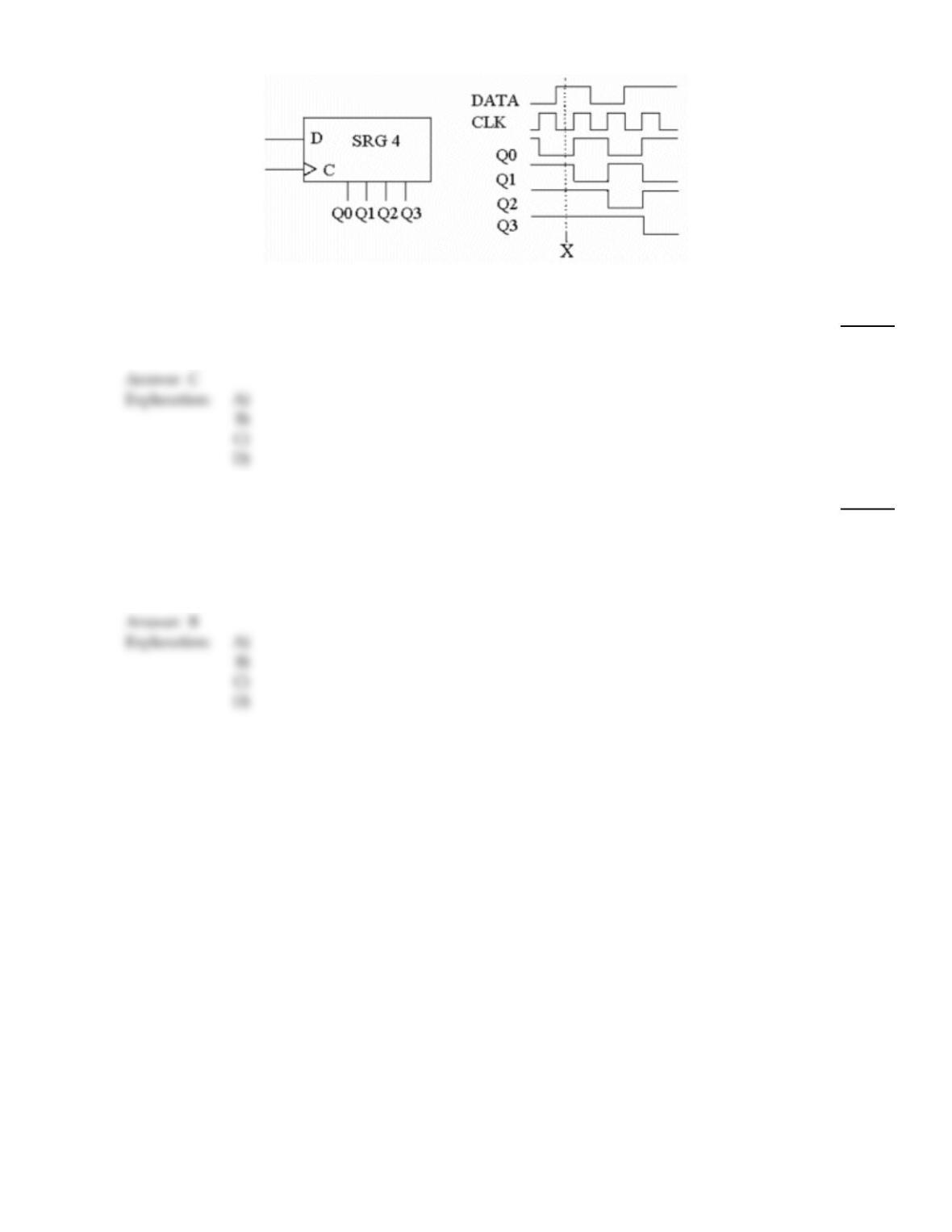
Figure 8–2
21)
Refer to the circuit and waveforms in Figure 8–2. What value is stored in the register at the end of
the fourth clock cycle?
21)
A)
0 1 1 0
B)
0 0 0 0
C)
0 1 0 1
D)
1 0 1 0
22)
When using an oscilloscope to troubleshoot a digital system, the instrument should be triggered by
________.
22)
A)
the AC line voltage
B)
the system clock
C)
line sync, in order to observe troublesome power line glitches
D)
the A channel or channel 1
11
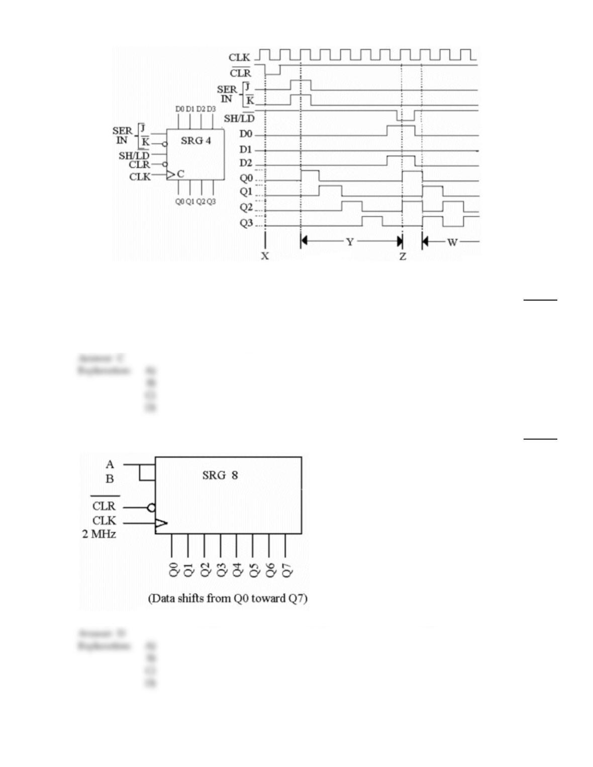
Figure 8–4
23)
Refer to Figure 8–4. What occurs at the point marked ‘Z’ on the timing diagram?
23)
A)
The register is reset.
B)
New serial data is loaded into the register.
C)
Parallel data is loaded into the register.
D)
The register is placed into a holding state.
24)
A serial data path needs a 2000 ns delay. Which output from the circuit below will provide the
correct delay?
24)
A)
Q0
B)
Q7
C)
Q1
D)
Q3
12
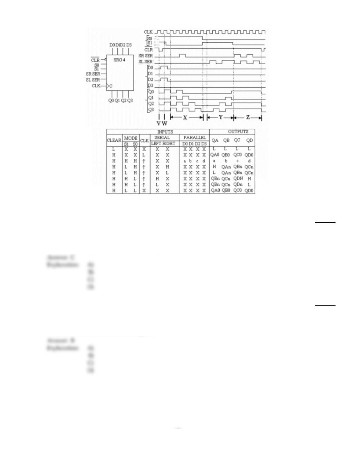
Figure 8–5
25)
Refer to Figure 8–5. What occurs at point ‘V’ on the timing diagram?
25)
A)
Data is loaded into the register from the parallel inputs.
B)
The parallel inputs are inhibited prevented from loading into the register.
C)
The outputs are cleared set to LOW.
D)
The serial inputs are loaded into the register.
26)
Refer to Figure 8–5. What occurs during the interval labeled ‘Z’ on the timing diagram?
26)
A)
Data is shifted left through the register.
B)
The operation of the register is inhibitedno changes occur on the outputs.
C)
Data is shifted right through the register.
D)
Serial data is entered into the register.
13
27)
Refer to Figure 8–5. What occurs during the interval labeled ‘X’ on the timing diagram?
27)
A)
Data is shifted right through the register.
B)
Data is shifted left through the register.
C)
Serial data is entered into the register.
D)
Parallel data is entered into the register.
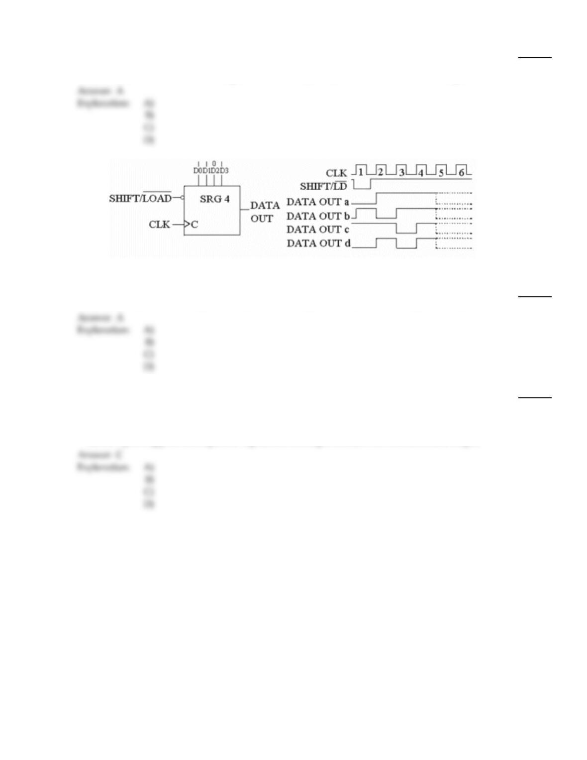
Figure 8–3
28)
Which of the DATA OUT waveforms shown in Figure 8–3 is correct?
28)
A)
DATA OUT b.
B)
DATA OUT a.
C)
DATA OUT c.
D)
DATA OUT d.
29)
In order to use a shift register as a counter, ________.
29)
A)
a serial–in, serial–out register must be used
B)
the register’s serial input is the counter input and the serial output is the counter output
C)
the serial output of the register is connected back to its serial input
D)
the input is applied to the parallel inputs and the output is taken from the serial data output
14
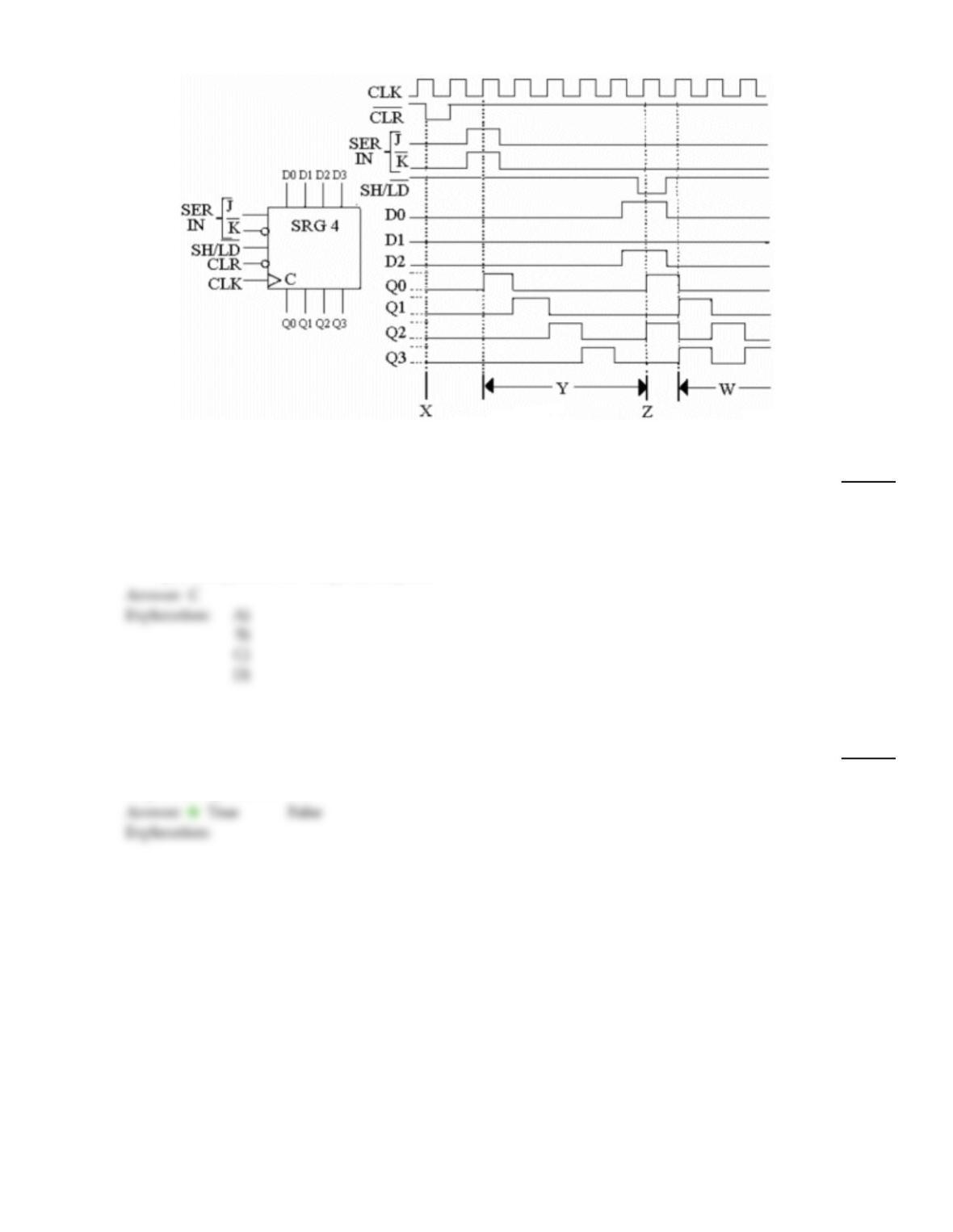
Figure 8–4
30)
Refer to Figure 8–4. What occurs during the interval marked ‘W’ on the timing diagram?
30)
A)
The register has just been cleared and the clock pulses are being toggled through the register.
B)
The data is shifted from the parallel inputs to the parallel outputs.
C)
Data is serially shifted through the register.
D)
The register has gone into the counter mode and is counting the value of the parallel data
previously stored on the parallel inputs.
TRUE/FALSE. Write ‘T’ if the statement is true and ‘F’ if the statement is false.
31)
One method of troubleshooting sequential logic circuits involves a process of “exercising” the
circuit being tested with a known input waveform and then checking the output to see if the proper
bit pattern is produced.
31)
15
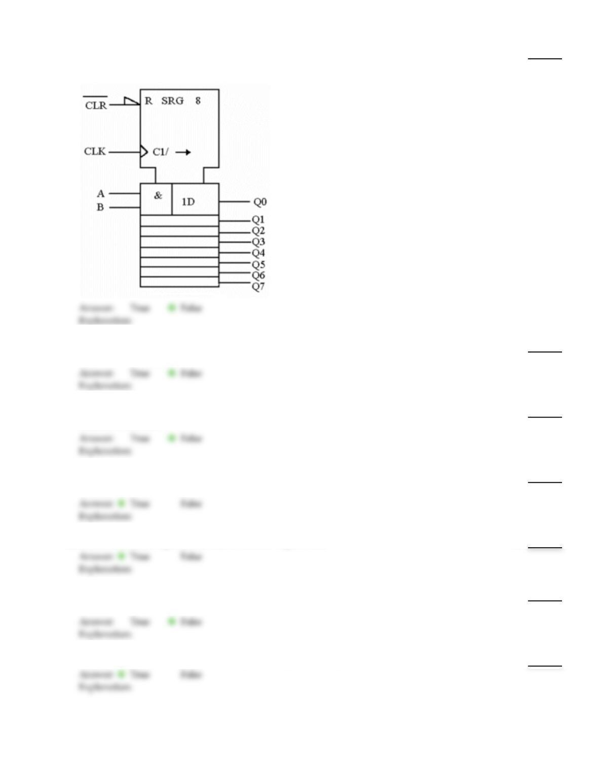
32)
The top section of the 74164 serial–in, parallel–out shift register shown indicates that only the first
DATA input section is controlled by the SRG 8 section.
32)
33)
An effective time delay device can be constructed by using the propagation delay characteristics of
a parallel shift register.
33)
34)
The serial–in, parallel–out shift register is used to transfer data one bit at a time from one parallel
data bus to another.
34)
35)
A parallel–in, serial–out shift register accepts all data bits simultaneously and transfers them out
one bit at a time.
35)
36)
Bidirectional shift registers can shift data either right or left.
36)
37)
Shift register counters often include reset logic circuits that clear them after a desired count is
reached.
37)
38)
Parallel–in, parallel–out registers have parallel input and output busses.
38)
16

39)
A serial–in, serial–out shift register is used to transfer data one bit at a time from one line of a
parallel bus to another.
39)
40)
Shift registers are used primarily to store and transfer data.
40)
17
Answer Key
Testname: C8
18