Exam
Name___________________________________
MULTIPLE CHOICE. Choose the one alternative that best completes the statement or answers the question.
1)
What is the indication of a short to ground in the output of a driving gate?
1)
A)
The node is stuck in the LOW state.
B)
There is a signal loss to all load gates.
C)
The affected node will be stuck in the HIGH state.
D)
Only the output of the defective gate is affected.
Figure 5–3
2)
Which circuit in Figure 5–3 represents the NAND implementation of an inverter?
2)
A)
Figure (A).
B)
Figure (B).
C)
Figure (C).
D)
Figure (D).
3)
What is the indication of a short on the input of a load gate?
3)
A)
Only the output of the defective gate is affected.
B)
There is a signal loss to all gates on the node.
C)
The affected node will be stuck in the LOW state.
D)
Both B and C are correct.
4)
How many gates, including inverters, are required to implement the equation, X = A + AB +AB,
after it is simplified using Boolean algebra?
4)
A)
1
B)
2
C)
3
D)
4
1
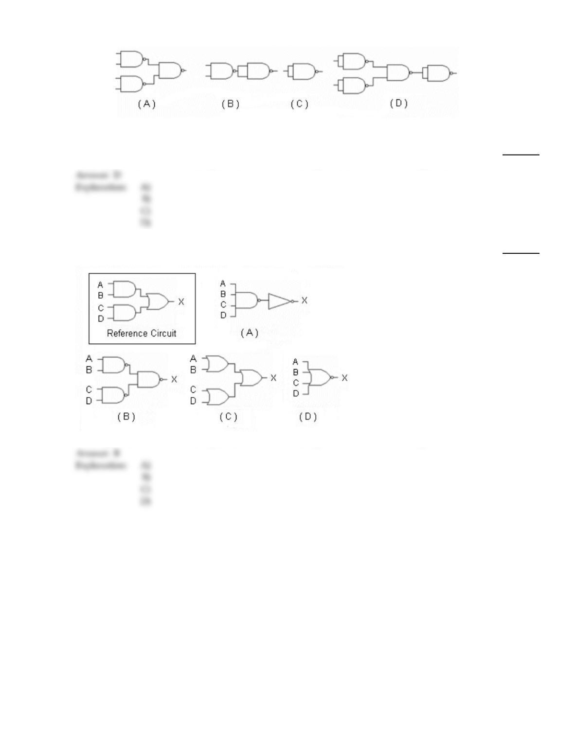
Figure 5–3
5)
Which circuit in Figure 5–3 represents the NAND implementation of a NOR gate?
5)
A)
Figure (A).
B)
Figure( B).
C)
Figure (C).
D)
Figure (D).
6)
Which circuit is the logical equivalent of the Reference Circuit?
6)
A)
Figure (A)
B)
Figure (B)
C)
Figure (C)
D)
Figure (D)
2
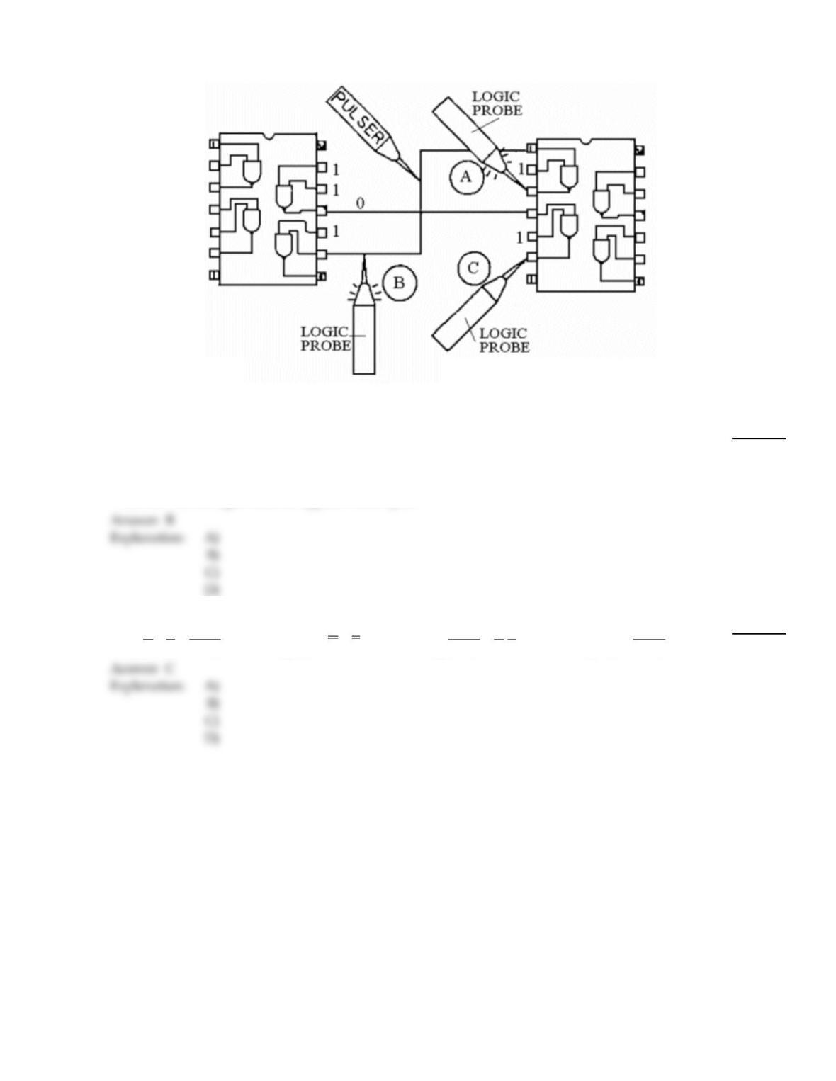
Figure 5–5
7)
Based on the indications of probe C in Figure 5–5, what, if anything, is wrong with the circuit?
7)
A)
The gate being tested has not been connected to Vcc and ground.
B)
Pin 6 on the right–hand IC is shorted to ground.
C)
The gate appears to be working correctly.
D)
Pin 5 on the right–hand IC appears to be open.
8)
The relationship between a NOR gate and a negative–AND gate is expressed by________.
8)
A)
A+B=A + B
B)
AB =A+B
C)
A + B =A B
D)
AB =A + B
C
3
B
9)
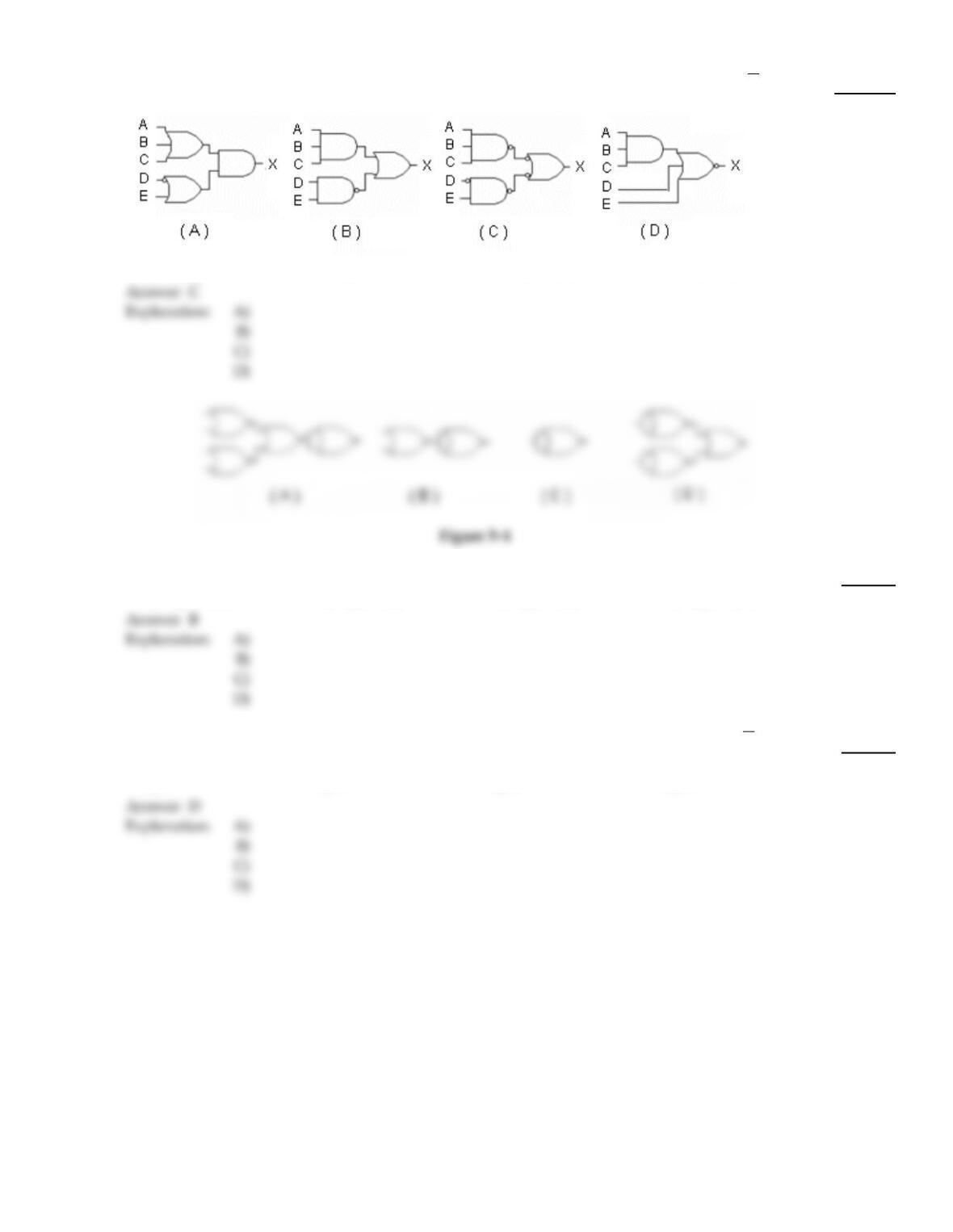
Which of the figures is the correct NAND logic implementation of the expression, X = ABC +DE?
9)
A)
Figure (A)
B)
Figure (B)
C)
Figure (C)
D)
Figure (D)
10)
Which circuit in Figure 5–4 represents the NOR implementation of an OR gate?
10)
A)
Figure (A)
B)
Figure (B)
C)
Figure (C)
D)
Figure (D)
11)
How many gates, including inverters, are required to implement the equation, X = A + AB +AB, as
it is written?
11)
A)
1
B)
2
C)
3
D)
4
4
12)
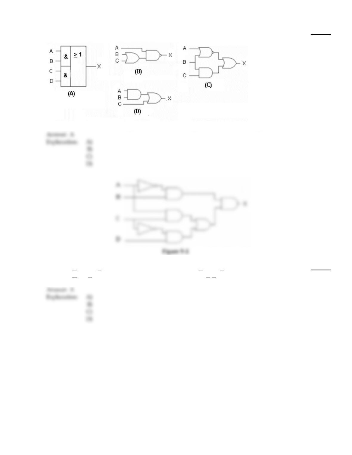
Which figure below represents AND–OR logic?
12)
A)
Figure (A)
B)
Figure (B)
C)
Figure (C)
D)
Figure (D)
13)
A correct logic expression for Figure 5–2 is ________.
13)
A)
X = (AB)(AC +CD)
B)
X =ABC + ACD
C)
X = (AB)(ACCD)
D)
X = ABC(CBD)
5
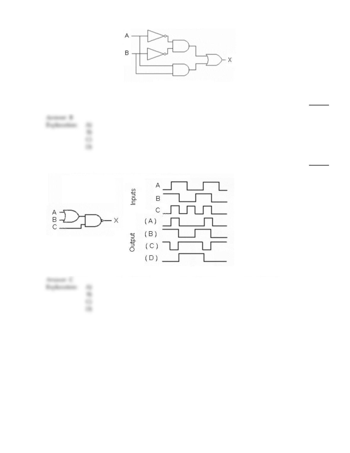
Figure 5–1
14)
What type of logic circuit is represented by Figure 5–1?
14)
A)
XOR
B)
XNOR
C)
XNAND
D)
XAND
15)
Which output waveform is correct for the circuit input waveforms shown?
15)
A)
Output (A)
B)
Output (B)
C)
Output (C)
D)
Output (D)
6
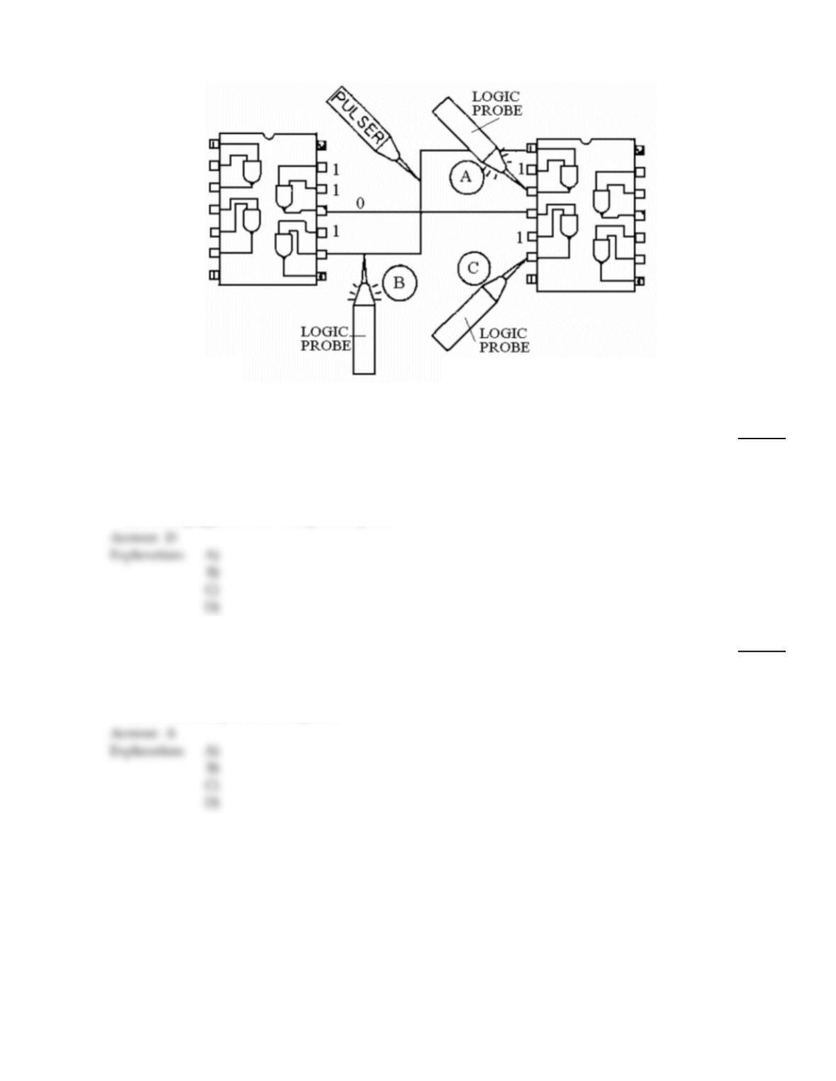
Figure 5–5
16)
Based on the indications of probe A in Figure 5–5, what, if anything, is wrong with the circuit?
16)
A)
The output appears to be shorted to Vcc, but is being pulsed by the pulser.
B)
The output appears to be LOW, but is being pulsed by the pulser.
C)
The logic probe is unable to determine the state of the circuit at that point and is blinking to
alert the technician to the problem.
D)
Nothing appears to be wrong at that point.
17)
The NAND gate is referred to as a “universal” gate, because it ________.
17)
A)
can be used to build all the other types of gates
B)
can be found in almost all digital circuits
C)
is used in all the countries of the world
D)
was the first gate to be integrated
7
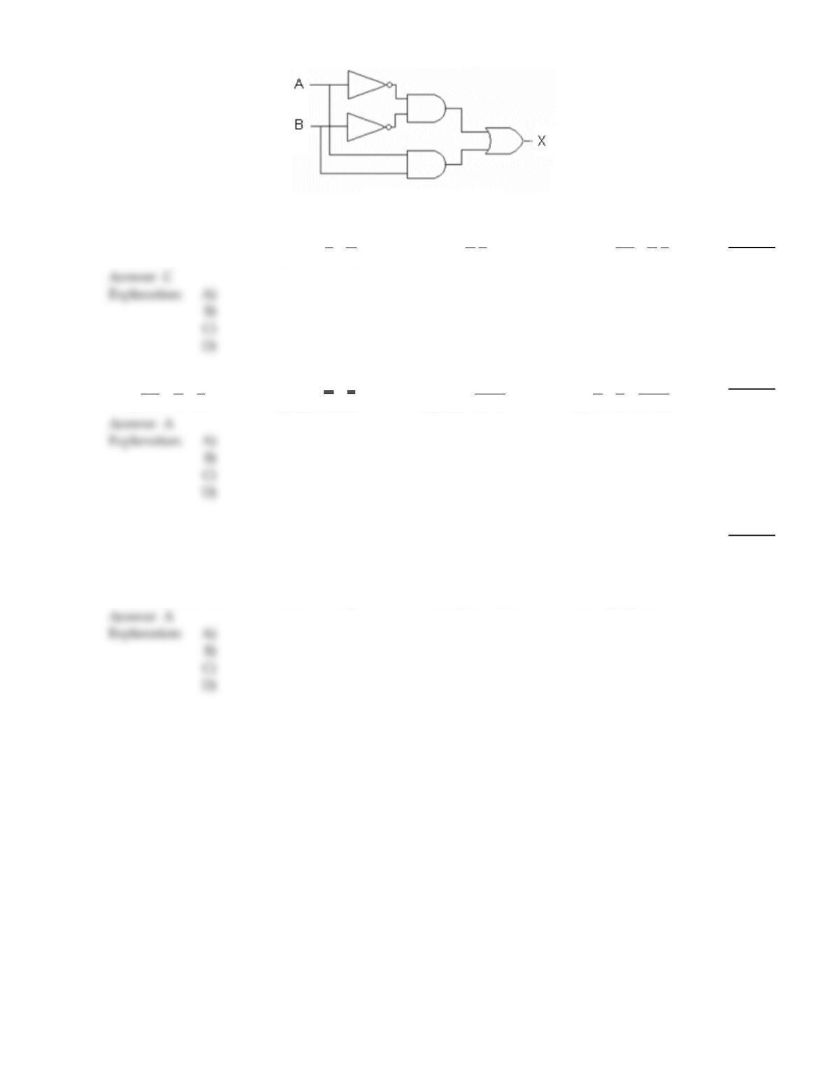
Figure 5–1
18)
Which of the following logic expressions represents the logic diagram in Figure 5–1?
18)
A)
X = AB + AB
B)
X = AB+AB
C)
X =A B + AB
D)
X =AB +A B
19)
The relationship between a NAND gate and a negative–OR gate is expressed by ________.
19)
A)
AB =A+B
B)
AB =A+B
C)
AB =A + B
D)
A+B=A + B
20)
An output gate is connected to four input gates; the circuit does not function. Preliminary tests with
a DMM indicate that power is applied; scope tests show that the primary input gate has a pulsing
signal, while the interconnecting node has no signal. The four load gates are all on different IC’s.
Which instrument will best help isolate the problem?
20)
A)
Current tracer
B)
Oscilloscope
C)
Logic analyzer
D)
Logic probe
8
21)
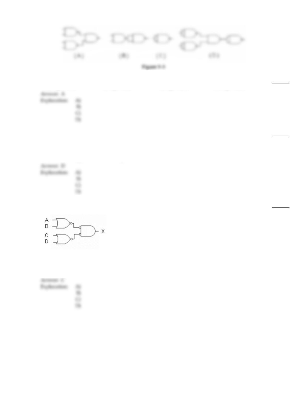
Which circuit in Figure 5–3 represents the NAND implementation of an AND–OR function?
21)
A)
Figure (A).
B)
Figure (B).
C)
Figure (C).
D)
Figure (D).
A
22)
What is the indication of an open in the output of a driving gate?
22)
A)
The affected node will be stuck in the LOW state.
B)
Only the output of the defective gate is affected.
C)
The affected node will be stuck in the HIGH state.
D)
There is a signal loss to all load gates.
D
23)
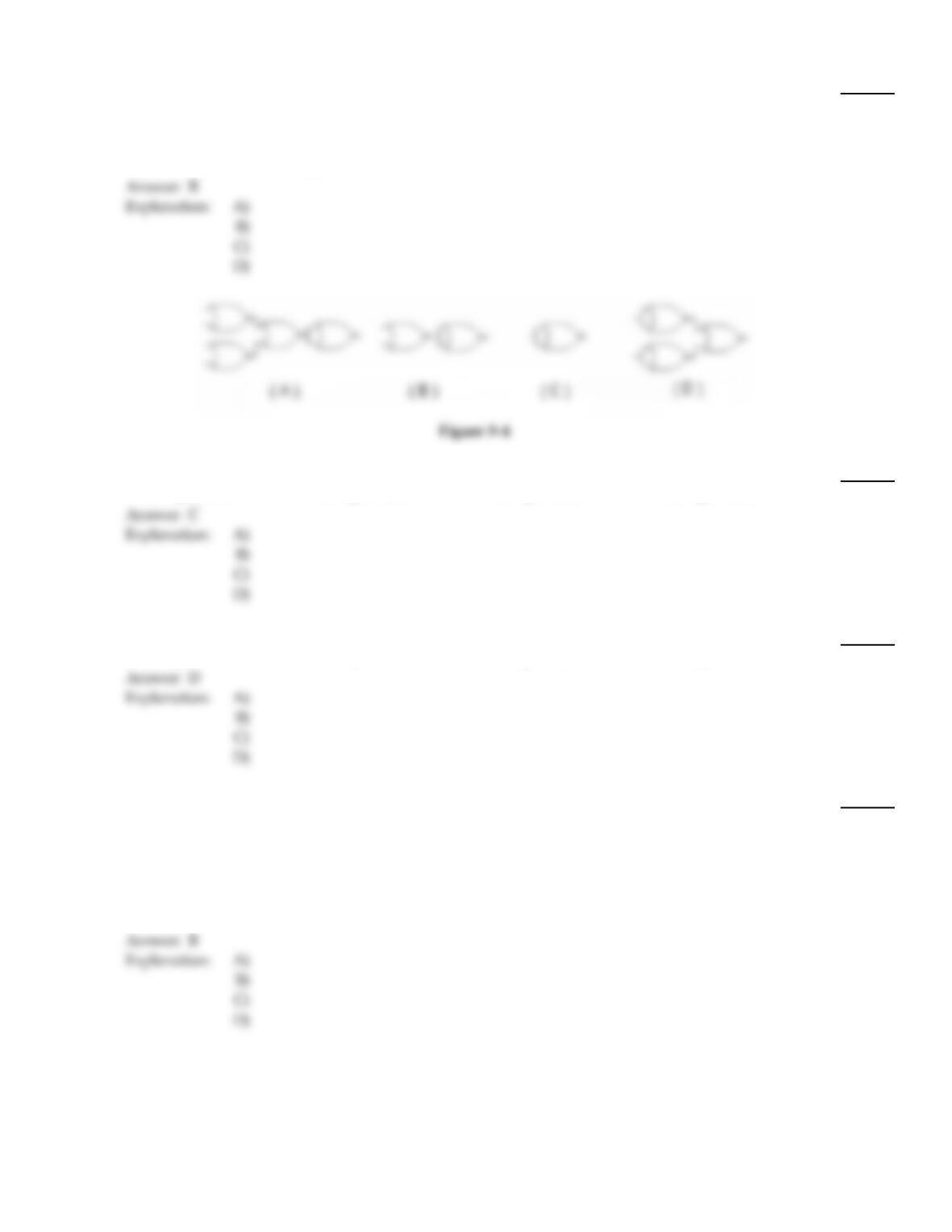
The reason that NOR logic networks are often drawn as shown in this figure, is ________.
23)
A)
to minimize the number of parts required
B)
to help make the transition to a K–map
C)
to make it easier to determine the logical output
D)
that it shows the actual gate arrangement
C
9
24)
The output of a gate has an internal short. A current tracer will ________.
24)
A)
be able to identify the defective load node
B)
probably not be able to locate the problem
C)
show whether the gate is shorted to Vcc or ground
D)
identify the defective gate
25)
Which circuit in Figure 5–4 represents the NOR implementation of an inverter?
25)
A)
Figure (A)
B)
Figure (B)
C)
Figure (C)
D)
Figure (D)
C
26)
Which circuit in Figure 5–4 represents the NOR implementation of an AND gate?
26)
A)
Figure (A)
B)
Figure (B)
C)
Figure (C)
D)
Figure (D)
D
27)
Why are multiple NAND gates often used in place of other single function gates?
27)
A)
NAND gates are packaged more densely on IC’s than other types of gates.
B)
It makes it possible to use spare portions of NAND IC packages to implement other logic
functions, perhaps reducing the total IC package count.
C)
It is easier to design logic circuits with a single gate type, since you only have to fully
understand how one type of gate works.
D)
NAND gates are cheaper than any other type of gate.
B
10
B
28)
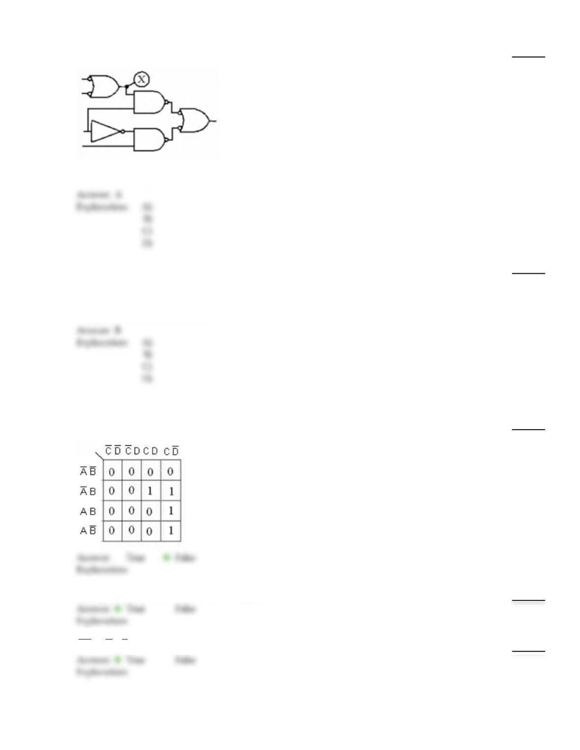
The point identified as ‘X’ in this figure is referred to as ________.
28)
A)
a node
B)
a tie point
C)
a reference point
D)
common
29)
When the inverted output of one gate is connected to the inverted input of another gate, ________.
29)
A)
a double inversion occurs and the signal is inverted
B)
the inversions cancel
C)
one inversion cancels the other and only a single inversion results
D)
all of the above are correct
TRUE/FALSE. Write ‘T’ if the statement is true and ‘F’ if the statement is false.
30)
The Karnaugh map below represents the expression, X = ACD + AB(CD + BC).
30)
31)
NOR gates can be used to construct AND gates.
31)
32)
AB =A+B
32)
11
33)
NAND gates cannot be used to construct NOR gates.
33)
34)
The NAND gate is an example of combinational logic.
34)
35)
X = ABC+ BCD is in the form of a sum–of–products expression.
35)
36)
The commonly accepted abbreviation for an exclusive–OR gate is XOR.
36)
37)
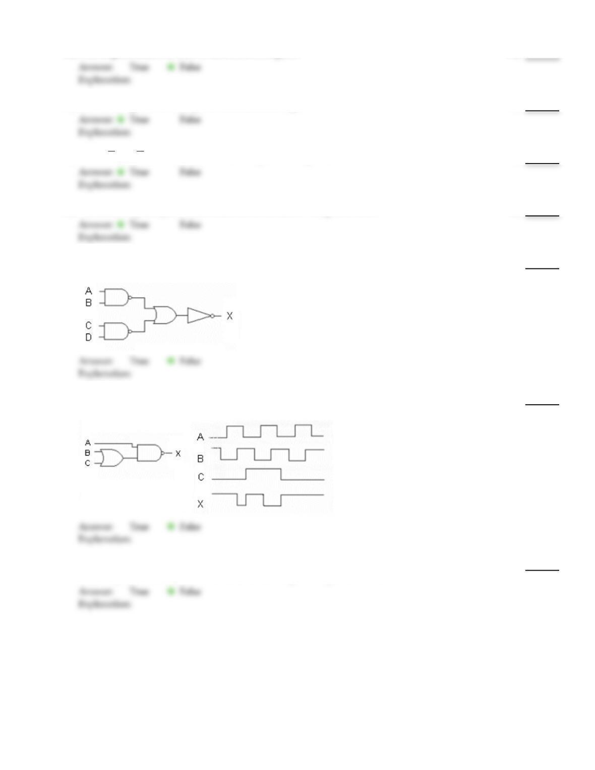
This circuit is an example of the implementation of AND–OR–INVERT logic.
37)
38)
The waveforms are correct for the logic circuit shown.
38)
39)
The effect of an inverted output being connected to the inverting input of another gate is to
effectively eliminate one of the inversions, resulting in a single inversion.
39)
12
Answer Key
Testname: C5
13