Chapter: Chapter 41
Learning Objectives
LO 41.1.0 Solve problems related to the electrical properties of metals.
LO 41.1.1 Identify the three basic properties of crystalline solids and sketch unit cells for them.
LO 41.1.2 Distinguish insulators, metals, and semiconductors.
LO 41.1.3 With sketches, explain the transition of an energy-level diagram for a single atom to
an energy-band diagram for many atoms.
LO 41.1.4 Draw a band–gap diagram for an insulator, indicting the filled and empty bands and
explaining what prevents the electrons from participating in a current.
LO 41.1.5 Draw a band–gap diagram for a metal, and explain what feature, in contrast to an
insulator, allows electrons to participate in a current.
LO 41.1.6 Identify the Fermi level, Fermi energy, and Fermi speed.
LO 41.1.7 Distinguish monovalent atoms, bivalent atoms, and trivalent atoms.
LO 41.1.8 For a conducting material, apply the relationships between the number density n of
conduction electrons to the material’s density, volume V, and molar mass M.
LO 41.1.9 Identify that in a metal’s partially filled band, thermal agitation can jump some of the
conduction electrons to higher energy levels.
LO 41.1.10 For a given energy level in a band, calculate the density of states N(E) and identify
that it is actually a double density (per volume and per energy).
LO 41.1.11 Find the number of states per unit volume in a range ΔE at height E in a band by
integrating N(E) over that range or, if ΔE is small relative to E, by evaluating the product N(E)
ΔE.
LO 41.1.12 For a given energy level, calculate the probability P(E) that the level is occupied by
electrons.
LO 41.1.13 Identify that the probability is 0.5 at the Fermi level.
LO 41.1.14 At a given energy level, calculate the density No (E) of occupied states.
LO 41.1.15 For a given range in energy levels, calculate the number of states and the number of
occupied states.
LO 41.1.16 Sketch graphs of the density of states N(E), occupancy probability P(E), and the
density of occupied states No (E), all versus height in a band.
LO 41.1.17 Apply the relationship between the Fermi energy EF and the number density of
conduction electrons n.
LO 41.2.0 Solve problems related to semiconductors and doping.
LO 41.2.1 Sketch a band–gap pattern for a semiconductor, identifying the conduction and
valence bands, conduction electrons, holes, and the energy gap.
LO 41.2.2 Compare the energy gap of a semiconductor with that of an insulator.
LO 41.2.3 Apply the relationship between a semiconductor’s energy gap and the wavelength of
light associated with a transition across the gap.
LO 41.2.4 Sketch the lattice structure for pure silicon and doped silicon.
LO 41.2.5 Identify holes, how they are produced, and how they move in an applied electric field.
LO 41.2.6 For metals and semiconductors, compare the resistivity ρ and the temperature
coefficient of resistivity α.
LO 41.2.7 Explain the procedure for producing n-type semiconductors and p-type
semiconductors.
LO 41.2.8 Apply the relationship between the number of conduction electrons in a pure material
and the number in the doped material.
LO 41.2.9 Identify donors and acceptors.
LO 41.2.10 Identify majority carriers and minority carriers.
LO 41.2.11 Explain the advantage of doping a semiconductor.
LO 41.3.0 Solve problems related to the p–n junction and the transistor
LO 41.3.1 Describe a p–n junction and outline how it works.
LO 41.3.2 Identify diffusion current, space charge, depletion zone, contact potential difference,
and drift current.
LO 41.3.3 Describe the functioning of a junction rectifier.
LO 41.3.4 Distinguish forward bias and back bias.
LO 41.3.5 Explain the general properties of a light-emitting diode, a photodiode, a junction laser,
and a MOSFET.
Multiple Choice
1. The Fermi-Dirac probability function P(E) varies between:
A) 0 and 1
B) 0 and infinity
C) 1 and infinity
D) –1 and 1
E) 0 and EF
2. We classify solids electrically according to three basic properties. What are they?
A) Conductivity, resistivity, and crystal structure
B) Resistivity, temperature coefficient of resistivity, and crystal structure
C) Resistivity, crystal structure, and number density of conduction electrons
D) Resistivity, temperature coefficient of resistivity, and number density of conduction electrons
E) Conductivity, temperature coefficient of resistivity, and crystal structure
3. The number density n of conduction electrons, the resistivity
, and the temperature
coefficient of resistivity α are given below for five materials. Which is a semiconductor?
A) n = 1029 m–3,
= 10–8 m, α = +10–3 K–1
B) n = 1028 m–3,
= 10–9 m, α = –10–3 K–1
C) n = 1028 m–3,
= 10–9 m, α = +10–3 K–1
D) n = 1015 m–3,
= 103 m, α = –10–2 K–1
E) n = 1022 m–3,
= 10–7 m, α = +10–3 K–1
4. A certain material has a resistivity of 7.8 103 m at room temperature, and its resistivity
increases as the temperature is raised by 100C. The material is most likely:
A) a metal
B) a pure semiconductor
C) a heavily doped semiconductor
D) an insulator
E) none of the above
5. A certain material has a resistivity of 7.8 103 m at room temperature, and its resistivity
decreases as the temperature is raised by 100C. The material is most likely:
A) a metal
B) a pure semiconductor
C) a heavily doped semiconductor
D) an insulator
E) none of the above
6. A certain material has a resistivity of 7.8 10–8 m at room temperature, and its resistivity
increases as the temperature is raised by 100C. The material is most likely:
A) a metal
B) a pure semiconductor
C) a heavily doped semiconductor
D) an insulator
E) none of the above
7. Which one of the following statements concerning electron energy bands in solids is true?
A) the bands occur as a direct consequence of the Fermi-Dirac distribution function
B) electrical conduction arises from the motion of electrons in completely filled bands
C) within a given band, all electron energy levels are equal to each other
D) an insulator has a large energy separation between the highest filled band and the lowest
empty band
E) only insulators have energy bands
8. If E0 and ET are the average energies of the “free” electrons in a metal at 0 K and room
temperature respectively, then the ratio ET/E0 is approximately:
A) 0
B) 1
C) 100
D) 106
E) infinity
9. The density of states for a metal depends primarily on:
A) the temperature
B) the energy associated with the state
C) the density of the metal
D) the volume of the sample
E) none of these
10. The Fermi energy of a metal depends primarily on:
A) the temperature
B) the volume of the sample
C) the mass density of the metal
D) the size of the sample
E) the number density of conduction electrons
11. The energy gap between the valence and conduction bands of an insulator is of the order:
A) 10–19 eV
B) 0.001 eV
C) 0.1 eV
D) 10 eV
E) 1000 eV
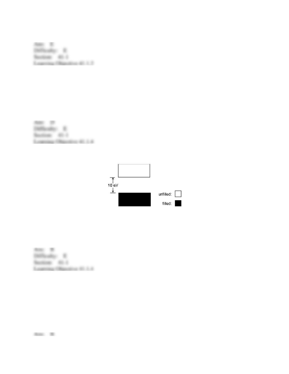
12. The energy level diagram shown applies to:
A) a conductor
B) an insulator
C) a semiconductor
D) an isolated atom
E) a free electron gas
13. Electrons in a full band do not contribute to the current when an electric field exists in a
solid because:
A) the field cannot exert a force on them
B) the individual contributions cancel each other
C) they are not moving
D) they make transitions to other bands
E) they leave the solid
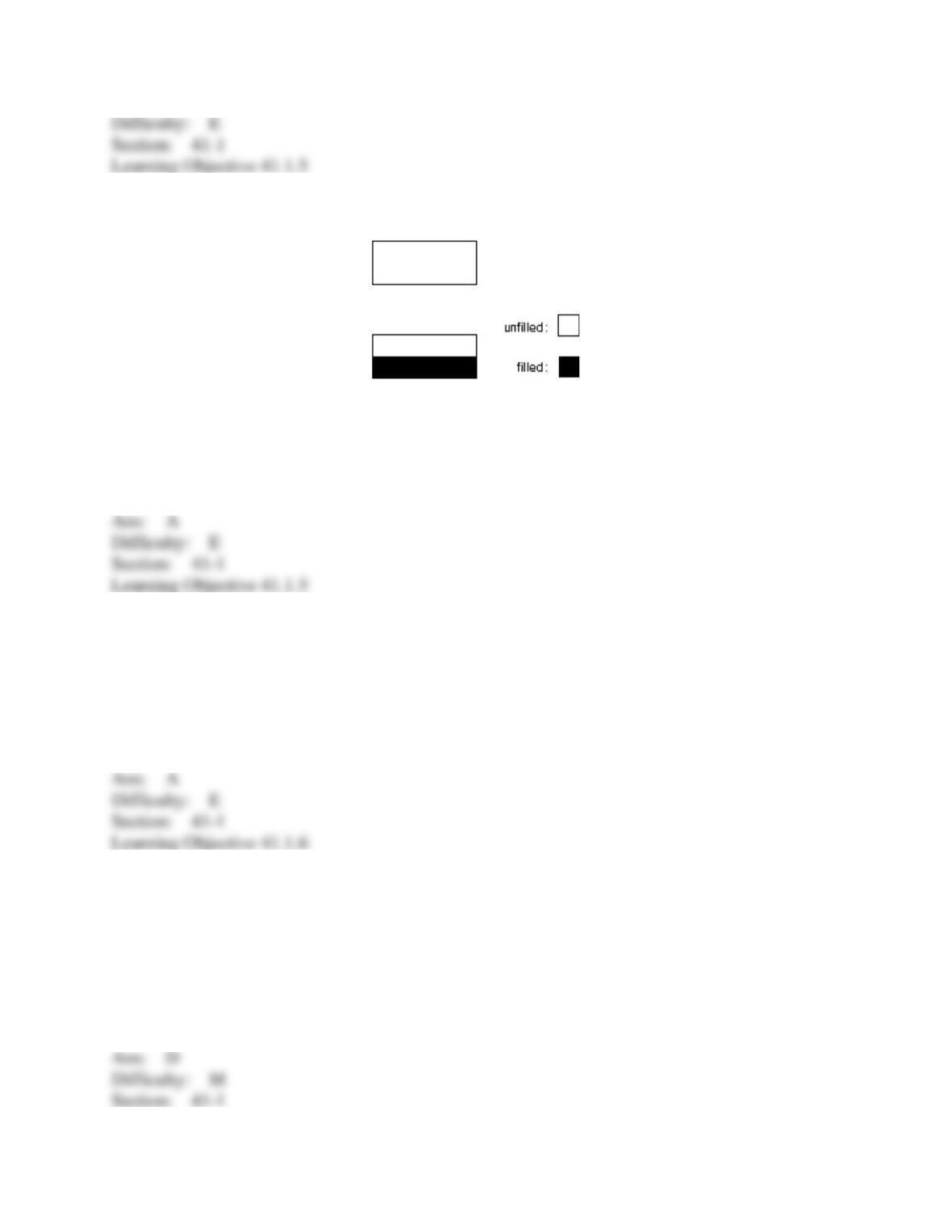
14. The energy level diagram shown applies to:
A) a conductor
B) an insulator
C) a semiconductor
D) an isolated molecule
E) an isolated atom
15. In a metal at 0 K, the Fermi energy is:
A) the highest energy of any electron
B) the lowest energy of any electron
C) the mean thermal energy of the electrons
D) the energy of the top of the valence band
E) the energy at the bottom of the conduction band
16. The speed of an electron with energy equal to the Fermi energy for copper is on the order
of:
A) 10–6 m/s
B) 10–1 m/s
C) 10 m/s
D) 106 m/s
E) 109 m/s
17. If ρm is the mass density of a conducting material, V its volume, M its molar mass, and NA
Avogadro’s number, the number density n of conduction electrons in the material is given by:
A) 𝑛 = 𝜌𝑚𝑉
𝑀𝑁𝐴
B) 𝑛 = 𝑁𝐴
𝑀𝜌𝑚
C) 𝑛 = 𝜌𝑚
𝑀𝑁𝐴
D) 𝑛 = 𝜌𝑚𝑁𝐴𝑉
E) 𝑛 = 𝑁𝐴𝑉
𝜌𝑚
18. Possible units for the density of states function N(E) are:
A) J/m3
B) 1/J
C) m–3
D) J–1 m–3
E) kg/m3
19. For a metal at absolute temperature T, with Fermi energy EF, the occupancy probability is
given by:
A) 𝑒(𝐸−𝐸𝐹)/𝑘𝑇
B) 𝑒−(𝐸−𝐸𝐹)/𝑘𝑇
C) 1
𝑒(𝐸−𝐸𝐹)/𝑘𝑇+1
D) 1
𝑒−(𝐸−𝐸𝐹)/𝑘𝑇+1
E) 1
𝑒(𝐸−𝐸𝐹)/𝑘𝑇−1
20. At T = 0 K the probability that a state 0.50 eV below the Fermi level is occupied is:
A) 0
B) 5.0 10–9
C) 5.0 10–6
D) 5.0 10–3
E) 1
21. At T = 0 K the probability that a state 0.50 eV above the Fermi level is occupied is:
A) 0
B) 5.0 10–9
C) 5.0 10–6
D) 5.0 10–3
E) 1
22. At room temperature, kT is about 0.0259 eV. The probability that a state 0.50 eV above the
Fermi level is occupied at room temperature is:
A) 1
B) 0.05
C) 0.026
D) 5.0 10–6
E) 4.1 10–9
23. At room temperature, kT is about 0.0259 eV. The probability that a state 0.50 eV below the
Fermi level is unoccupied at room temperature is:
A) 1
B) 0.05
C) 0.026
D) 5.0 10–6
E) 4.1 10–9
24. The occupancy probability for a state with energy equal to the Fermi energy is:
A) 0
B) 0.5
C) 1
D) 1.5
E) 2
25. If the density of states is N(E) and the occupancy probability is P(E), then the density of
unoccupied states is:
A) N(E) + P(E)
B) N(E)/P(E)
C) N(E) – P(E)
D) N(E)P(E)
E) N(E)(1 − P(E))
26. Magnesium has 8.6 x 1028 conduction electrons per cubic meter. What is the Fermi energy
for magnesium?
A) 1.8 eV
B) 7.1 eV
C) 9.1 eV
D) 22 eV
E) 28 eV
27. A pure semiconductor at room temperature has:
A) more electrons/m3 in its conduction band than holes/m3 in its valence band
B) more electrons/m3 in its conduction band than a typical metal
C) more electrons/m3 in its valence band than at T = 0 K
D) more holes/m3 in its valence band than electrons/m3 in its valence band
E) none of the above
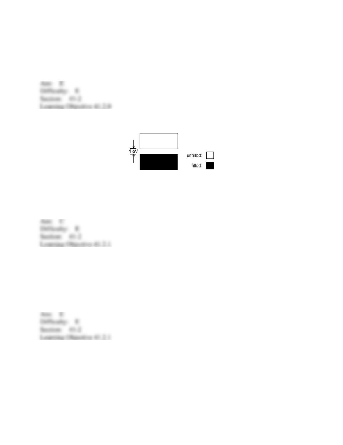
28. The energy level diagram shown applies to:
A) a conductor
B) an insulator
C) a semiconductor
D) an isolated molecule
E) an isolated atom
29. For a pure semiconductor the Fermi level is:
A) in the conduction band
B) well above the conduction band
C) in the valence band
D) well below the valence band
E) near the center of the gap between the valence and conduction bands
30. Compared to an insulator, the energy gap of a semiconductor is:
A) much smaller
B) about the same
C) much larger
D) full of holes
E) full of charge carriers
31. A hole refers to:
A) a proton
B) a positively charged electron
C) an electron which has somehow lost its charge
D) a microscopic defect in a solid
E) the absence of an electron in an otherwise filled band
32. For a metal at room temperature the temperature coefficient of resistivity is determined
primarily by:
A) the number of electrons in the conduction band
B) the number of impurity atoms
C) the binding energy of outer shell electrons
D) collisions between conduction electrons and atoms
E) none of the above
33. For a pure semiconductor at room temperature the temperature coefficient of resistivity is
determined primarily by:
A) the number of electrons in the conduction band
B) the number of replacement atoms
C) the binding energy of outer shell electrons
D) collisions between conduction electrons and atoms
E) none of the above
34. A given doped semiconductor can be identified as p or n type by:
A) measuring its electrical conductivity
B) measuring its magnetic susceptibility
C) measuring its coefficient of resistivity
D) measuring its heat capacity
E) performing a Hall effect experiment
35. Compared to the number of conduction electrons in pure silicon, the number of conduction
electrons in doped silicon is:
A) lower by about a factor of 10
B) about the same
C) higher by about a factor of 10
D) higher by about a factor of 1000
E) higher by about a factor or 1,000,000
36. Donor atoms introduced into a pure semiconductor at room temperature:
A) increase the number of electrons in the conduction band
B) increase the number of holes in the valence band
C) lower the Fermi level
D) increase the electrical resistivity
E) none of the above
37. Acceptor atoms introduced into a pure semiconductor at room temperature:
A) increase the number of electrons in the conduction band
B) increase the number of holes in the valence band
C) lower the Fermi level
D) increase the electrical resistivity
E) none of the above
38. An acceptor replacement atom in silicon might have ______ electrons in its outer shell.
A) 3
B) 4
C) 5
D) 6
E) 7
39. A donor replacement atom in silicon might have ______ electrons in its outer shell.
A) 1
B) 2
C) 3
D) 4
E) 5
40. The contact electric field in the depletion region of a p–n junction is produced by:
A) electrons in the conduction band alone
B) holes in the valence band alone
C) electrons and holes together
D) charged replacement atoms
E) an applied bias potential difference
41. In an unbiased p–n junction:
A) the electric potential vanishes everywhere
B) the electric field vanishes everywhere
C) the drift current vanishes everywhere
D) the diffusion current vanishes everywhere
E) the diffusion and drift currents cancel each other
42. For an unbiased p–n junction, the energy at the bottom of the conduction band on the n side
is:
A) higher than the energy at the bottom of the conduction band on the p side
B) lower than the energy at the bottom of the conduction band on the p side
C) lower than energy at the top of the valence band on the n side
D) lower than energy at the top of the valence band on the p side
E) the same as the energy at the bottom of the conduction band on the p side
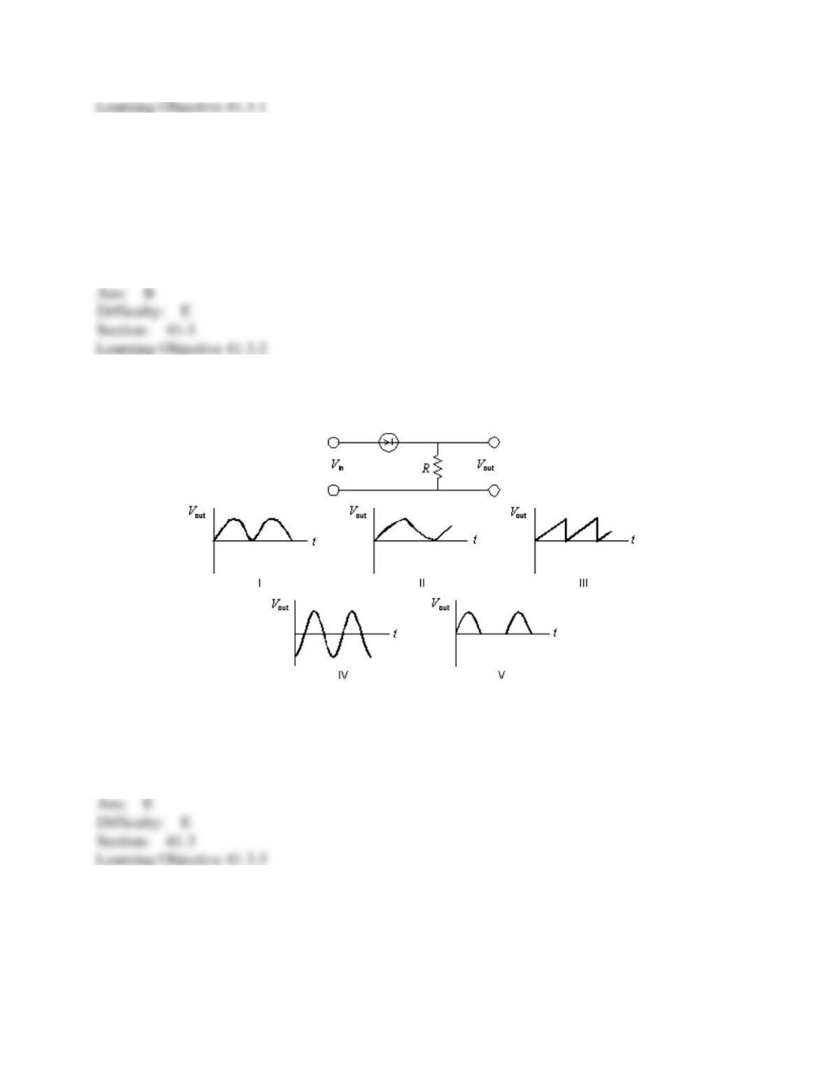
43. A sinusoidal potential difference Vin = Vmsin(
t) is applied to the p–n junction as shown.
Which graph correctly shows Vout as a function of time?
A) I
B) II
C) III
D) IV
E) V
44. Application of a forward bias to a p–n junction:
A) narrows the depletion zone
B) increases the electric field in the depletion zone
C) increases the potential difference across the depletion zone
D) increases the number of donors on the n side
E) decreases the number of donors on the n side
45. Application of a forward bias to a p–n junction:
A) increases the drift current in the depletion zone
B) increases the diffusion current in the depletion zone
C) decreases the drift current on the p side outside the depletion zone
D) decreases the drift current on the n side outside the depletion zone
E) does not change the current anywhere
46. When a forward bias is applied to a p–n junction the concentration of electrons on the p
side:
A) increases slightly
B) increases dramatically
C) decreases slightly
D) decreases dramatically
E) does not change
47. Which of the following is NOT true when a back bias is applied to a p–n junction?
A) Electrons flow from the p to the n side
B) Holes flow from the p to the n side
C) The electric field in the depletion zone increases
D) The potential difference across the depletion zone increases
E) The depletion zone narrows
48. Switch S is closed to apply a potential difference V across a p–n junction as shown. Relative
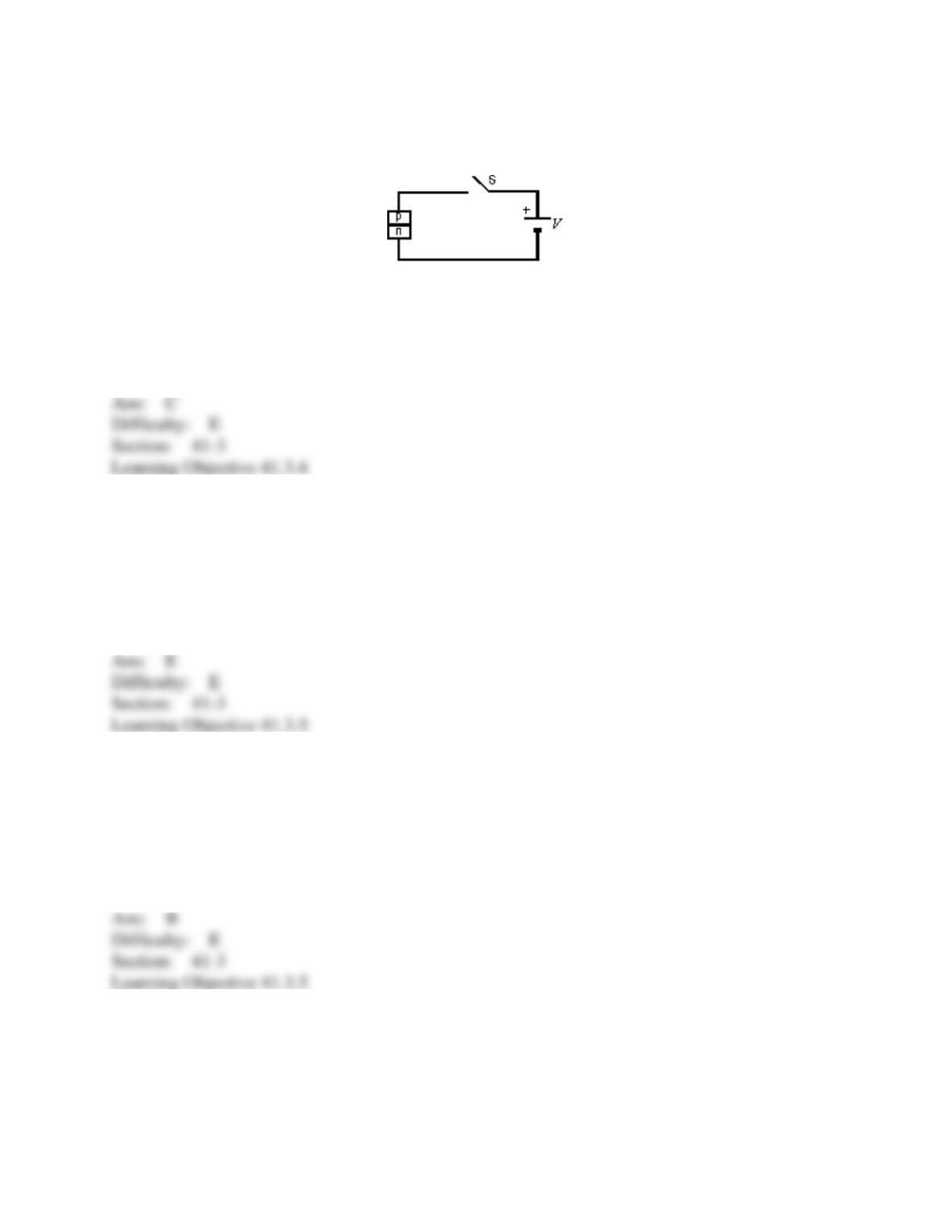
to the energy levels of the n-type material, with the switch open, the electron levels of the p-type
material are:
A) unchanged
B) lowered by the amount e–Ve/kT
C) lowered by the amount Ve
D) raised by the amount e–Ve/kT
E) raised by the amount Ve
49. “LED” stands for:
A) Less Energy Donated
B) Light Emitting Degrader
C) Luminescent Energy Diode
D) Laser Emitting Device
E) none of the above
50. A light emitting diode emits light when:
A) electrons are excited from the valence to the conduction band
B) electrons from the conduction band recombine with holes from the valence band
C) electrons collide with atoms
D) electrons are accelerated by the electric field in the depletion region
E) the junction gets hot
51. The gap between the valence and conduction bands of a certain semiconductor is 0.85eV.
When this semiconductor is used to form a light emitting diode, the wavelength of the light
emitted:
A) is in a range above 1.5 10–6 m
B) is in a range below 1.5 10–6 m
C) is always 1.5 10–6 m
D) is in a range centered on 1.5 10–6 m
E) has nothing to do with the gap