Exam
Name___________________________________
MULTIPLE CHOICE. Choose the one alternative that best completes the statement or answers the question.
1)
A logic gate draws 10mA when its output is HIGH and 20mA when its output is LOW. When
operating from a 12V supply with a 10% duty cycle the average power dissipation will be
________.
1)
A)
324mW
B)
228mW
C)
360mW
D)
180mW
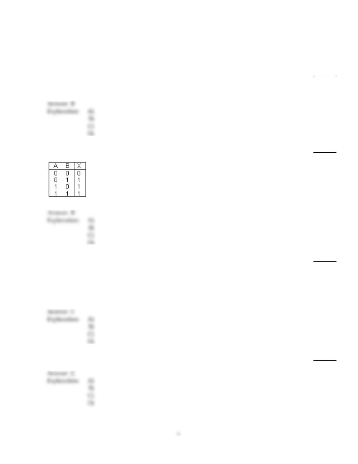
2)
The truth table below describes a(n) ________.
2)
A)
AND gate
B)
OR gate
C)
NOR gate
D)
NAND gate
3)
The difference between a PLA and a PAL is ________.
3)
A)
the PAL has a programmable OR plane and a programmable AND plane while the PLA only
has a programmable AND plane
B)
the PAL has more possible product terms than the PLA
C)
the PLA has a programmable OR plane and a programmable AND plane while the PAL only
has a programmable AND plane
D)
PALs and PLAs are the same thing.
4)
The ________ in a VHDL program describes its logic operation.
4)
A)
hardware
B)
source
C)
architecture
D)
entity
5)
HDL stands for ________.
5)
A)
hardwired digital logic
B)
hardware description language
C)
hardwire descriptive logic
D)
none of the above
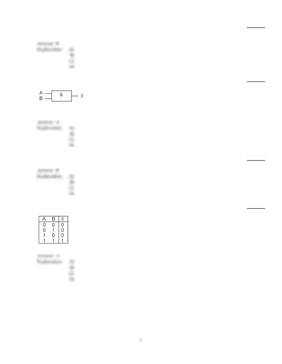
6)
The symbol below represents a(n) ________.
6)
A)
AND gate
B)
NAND gate
C)
OR gate
D)
none of the above
7)
Which of the following is not a type of SPLD?
7)
A)
GAL
B)
RAM
C)
PROM
D)
PLA
8)
The truth table below describes a(n) ________.
8)
A)
AND gate
B)
OR gate
C)
NOR gate
D)
NAND gate
9)
The timing diagram below is correct for a 2–input ________ gate.
9)
A)
NOR
B)
AND
C)
Exclusive–NOR
D)
OR
10)
The symbol below represents a(n) ________.
10)
A)
AND gate
B)
NAND gate
C)
OR gate
D)
Inverter
11)
The truth table below describes a(n) ________.
11)
A)
AND gate
B)
OR gate
C)
NOR gate
D)
NAND gate
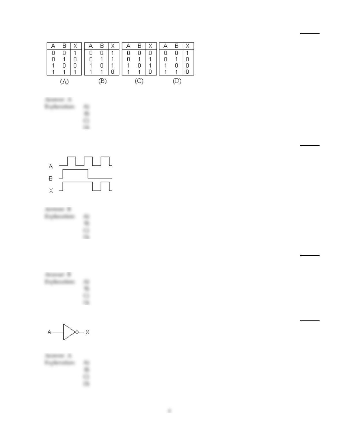
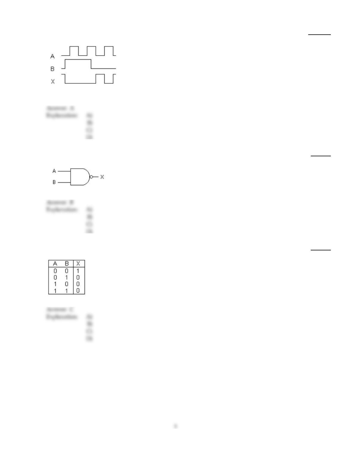
12)
Which of the truth tables below describes the Exclusive–NOR gate?
12)
A)
(A)
B)
(B)
C)
(C)
D)
(D)
13)
The timing diagram below is correct for a 2–input ________ gate.
13)
A)
AND
B)
OR
C)
NAND
D)
Exclusive–OR
14)
What programmable arrays are in PLD’s?
14)
A)
NOR arrays
B)
OR arrays and AND arrays
C)
AND arrays only
D)
OR arrays only
15)
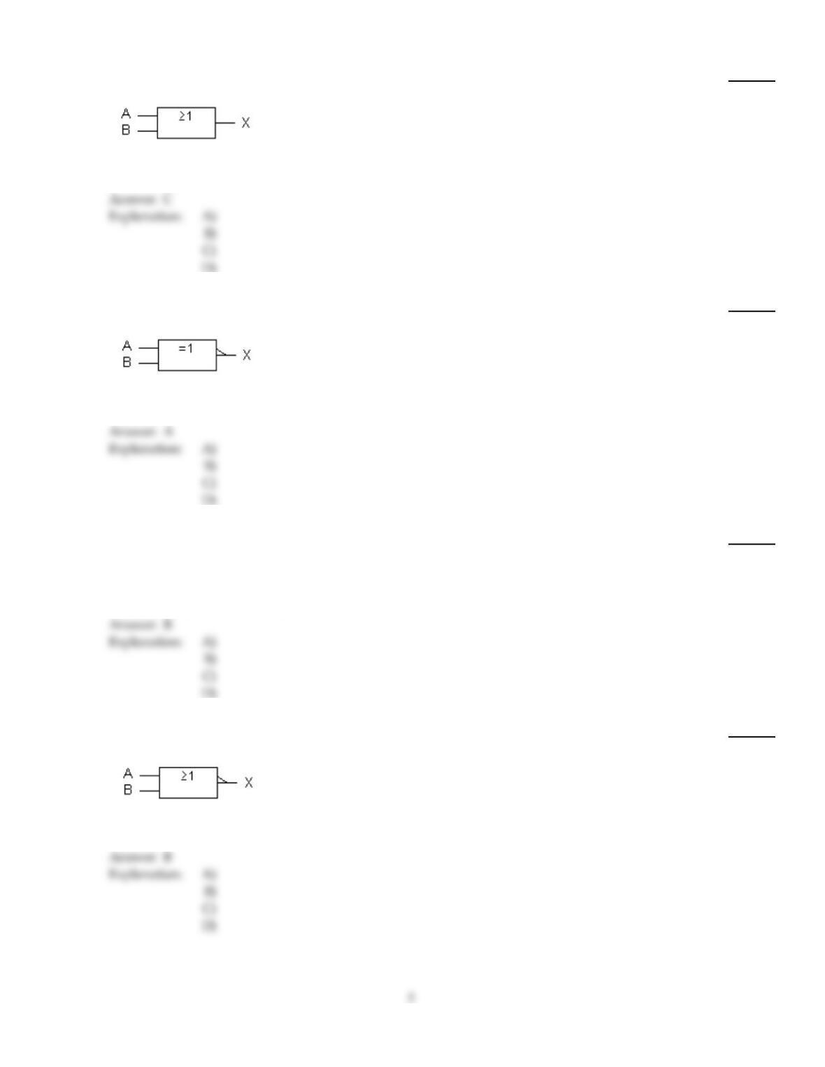
The symbol below represents a(n) ________.
15)
A)
Inverter
B)
NAND gate
C)
AND gate
D)
OR gate
16)
The symbol below represents a(n) ________.
16)
A)
AND gate
B)
Inverter
C)
OR gate
D)
none of the above
17)
The symbol below represents a(n) ________.
17)
A)
Exclusive–NOR gate
B)
Exclusive–OR gate
C)
NAND gate
D)
NOR gate
18)
When an open occurs on the input to a bipolar logic device, the output will ________.
18)
A)
go HIGH, since full voltage appears across an open
B)
react to the open input as if it were a HIGH input
C)
go LOW, because there is no current in an open circuit
D)
still be good, if only the good inputs are used
19)
The symbol below represents a(n) ________.
19)
A)
NAND gate
B)
NOR gate
C)
inverter
D)
Exclusive–NOR gate
20)
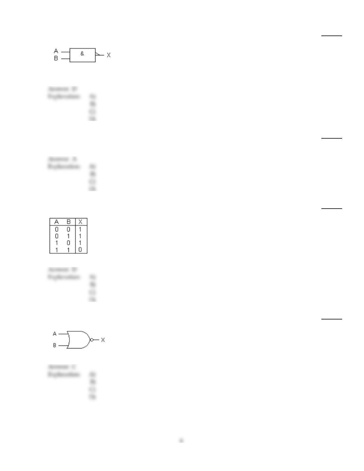
The symbol below represents a(n) ________.
20)
A)
Exclusive–NOR gate
B)
inverter
C)
NOR gate
D)
NAND gate
21)
IC’s with a ________ prefix have a broad operating temperature range and are generally used by
the military.
21)
A)
54
B)
TTL
C)
74
D)
2N
22)
The truth table below describes a(n) ________.
22)
A)
AND gate
B)
OR gate
C)
NOR gate
D)
NAND gate
23)
The symbol below represents a(n) ________.
23)
A)
NAND gate
B)
OR gate
C)
NOR gate
D)
AND gate
24)
The ________ in a VHDL program defines the logic element and its inputs/outputs or ports.
24)
A)
source
B)
architecture
C)
entity
D)
hardware
25)
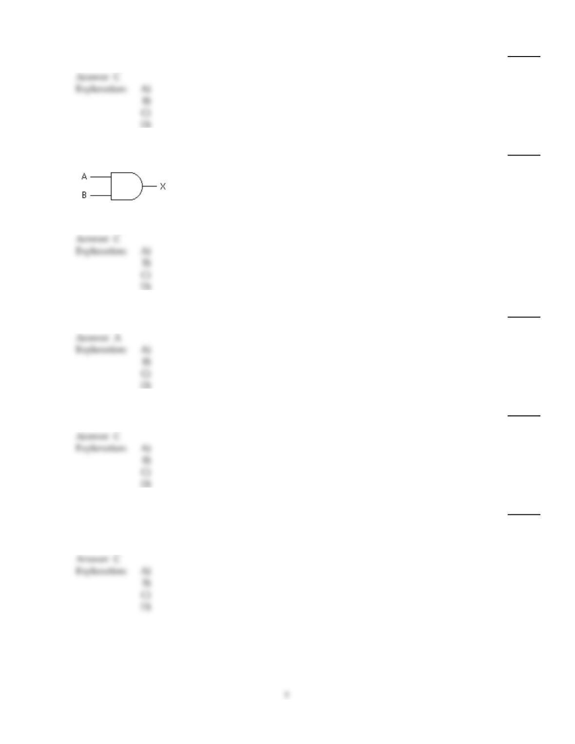
The symbol below represents a(n) ________.
25)
A)
NAND gate
B)
OR gate
C)
AND gate
D)
none of the above
26)
The ________ series of IC’s are pin, function and voltage–level compatible with the 74 series IC’s.
26)
A)
HCT
B)
2N
C)
ALS
D)
CMOS
27)
A ________ IC comes with logic functions that are not programmed in and cannot be altered.
27)
A)
microcontroller
B)
HDL
C)
fixed–function
D)
VHDL
28)
HDLs differ from ________ in that they include ways of describing propagation times and other
logic characteristics.
28)
A)
software programming languages
B)
software digital logic
C)
software description languages
D)
none of the above
29)
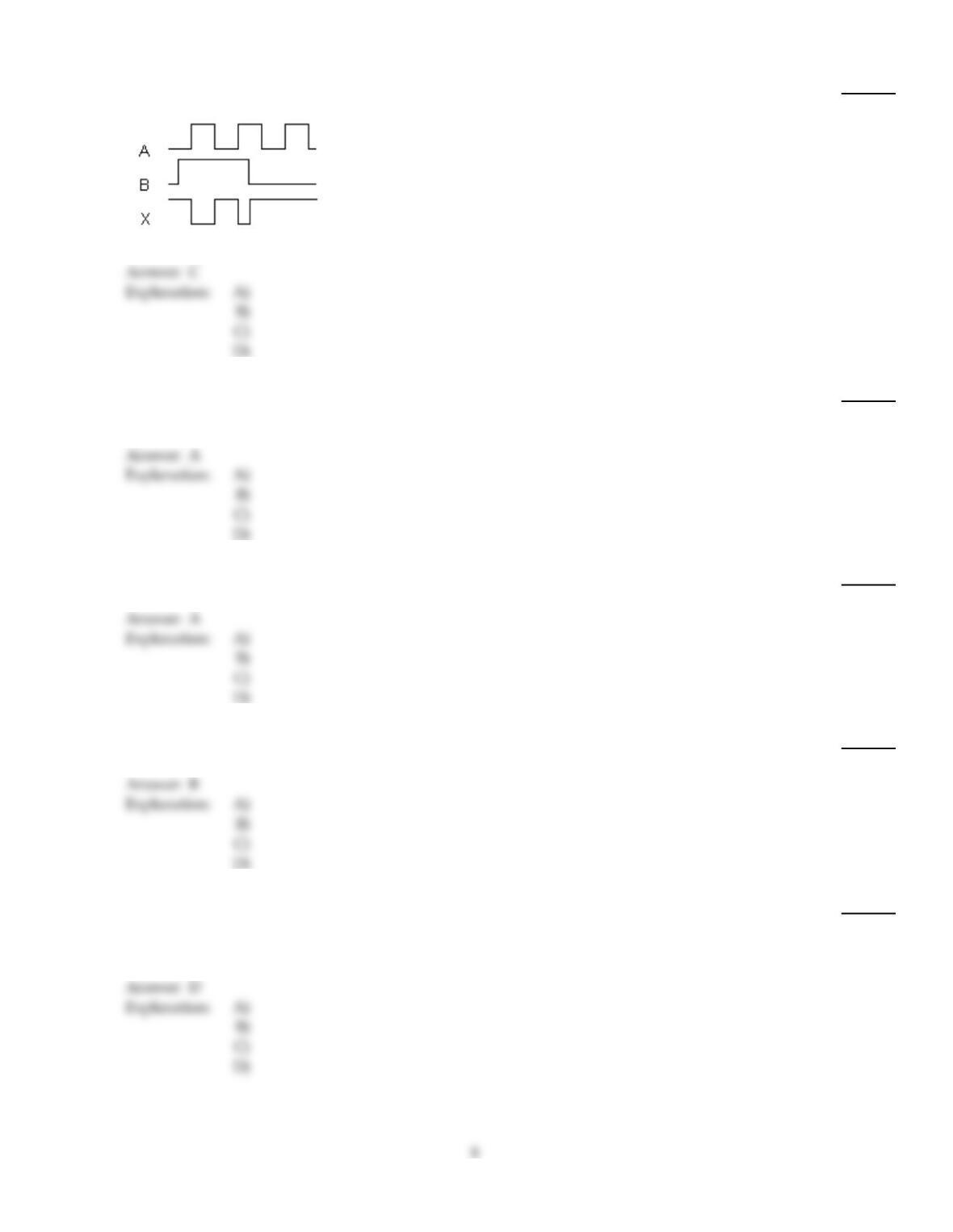
The timing diagram below is correct for a 2–input ________ gate.
29)
A)
AND
B)
OR
C)
NAND
D)
Exclusive–OR
30)
The term “hex inverter” refers to ________.
30)
A)
six inverters in a single package
B)
an inverter which has six inputs
C)
an inverter that has a history of failure
D)
a six–input symbolic logic device
31)
The fanout for standard bipolar logic devices is ________.
31)
A)
10
B)
2
C)
5
D)
1
32)
What technology allows a GAL to be reprogrammed again and again?
32)
A)
NMOS
B)
E2CMOS
C)
TTL
D)
CMOS
33)
An AND gate is checked for operation and the following readings are taken on the gate: input A =
0.2 V, input B = 4.5 V, input C = 0.4 V, output = 4.9 V. What might be wrong with the gate?
33)
A)
The output is too low: it should be 5 V.
B)
Input C is too high.
C)
Nothing is wrong with the gate.
D)
The output is stuck high; the chip is bad.
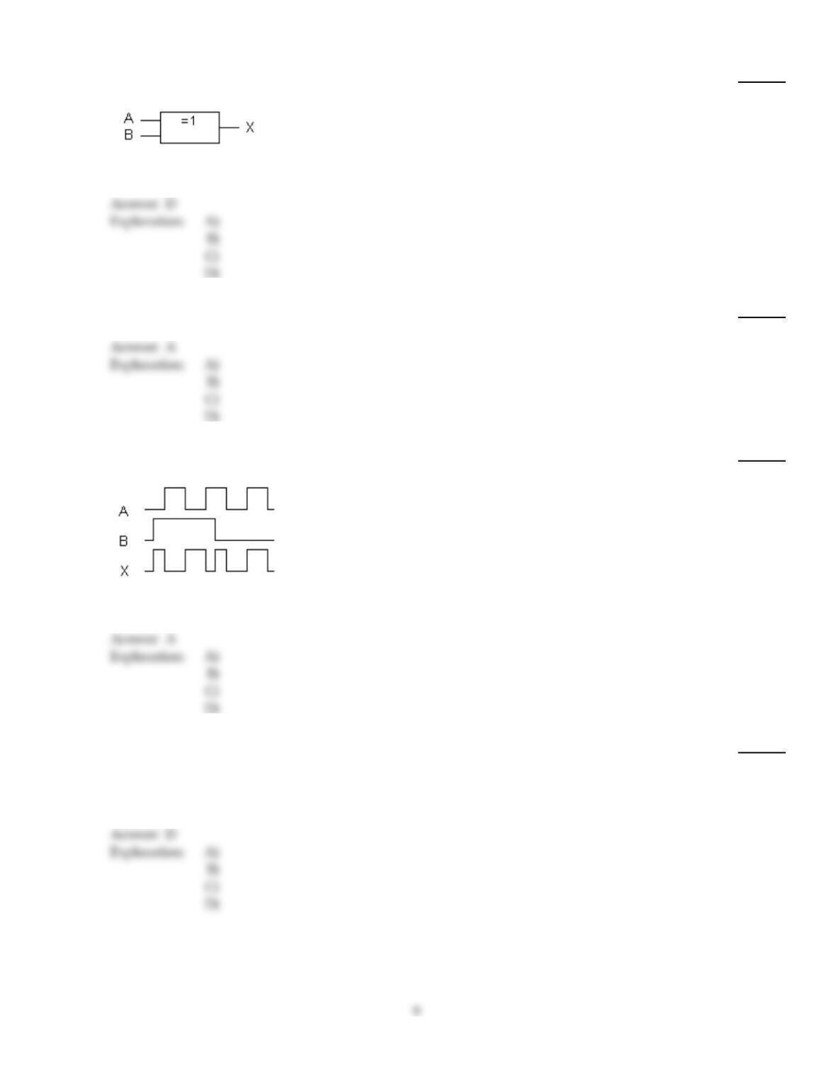
34)
The symbol below represents a(n) ________.
34)
A)
AND gate
B)
OR gate
C)
NAND gate
D)
Exclusive–OR gate
35)
Which type of gate can be used to add two bits?
35)
A)
XOR
B)
XNAND
C)
NAND
D)
NOR
A
36)
The timing diagram below is correct for a 2–input ________ gate.
36)
A)
Exclusive–OR
B)
Exclusive–NOR
C)
AND
D)
NAND
A
37)
When an open occurs on the input of a CMOS gate, the output will ________.
37)
A)
go HIGH, since full voltage appears across an open
B)
be treated as if the open input were a HIGH
C)
go LOW, because there is no current in an open circuit
D)
be unpredictable; it may go HIGH or LOW
D
D
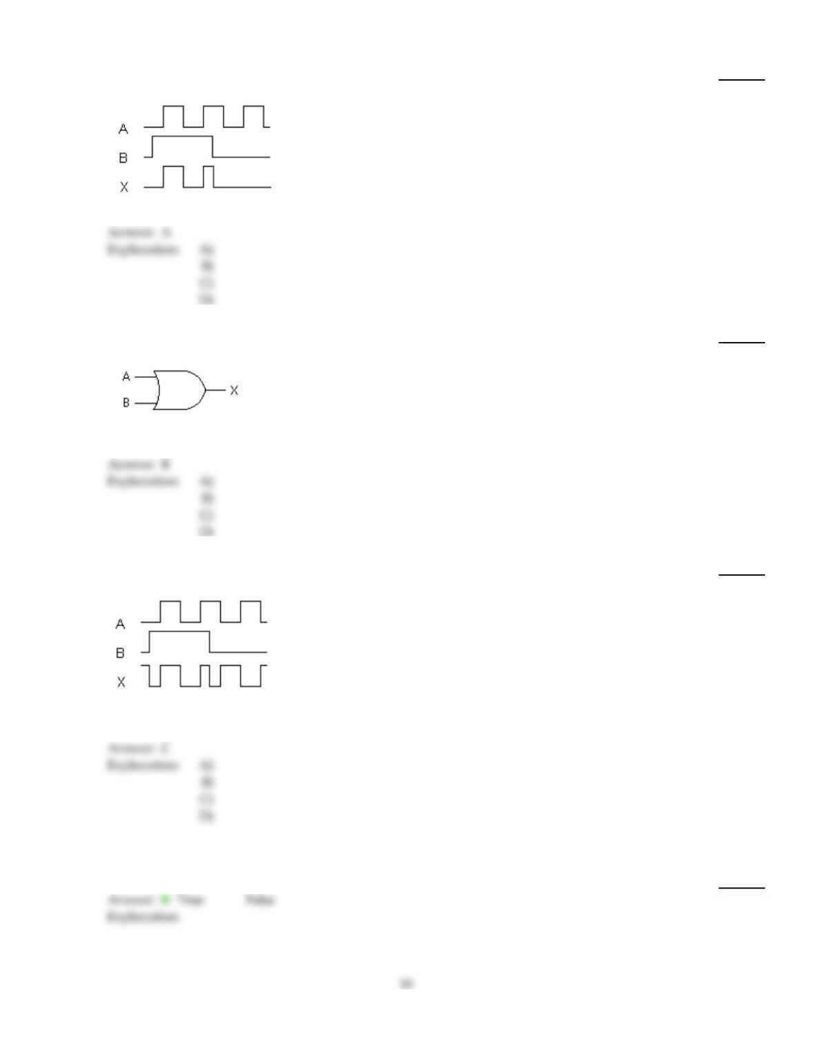
38)
The timing diagram below is correct for a 2–input ________ gate.
38)
A)
AND
B)
OR
C)
NAND
D)
Exclusive–OR
39)
The symbol below represents a(n) ________.
39)
A)
Inverter
B)
OR gate
C)
AND gate
D)
none of the above
40)
The timing diagram below is correct for a 2–input ________ gate.
40)
A)
NAND
B)
AND
C)
Exclusive–NOR
D)
Exclusive–OR
TRUE/FALSE. Write ‘T’ if the statement is true and ‘F’ if the statement is false.
41)
When the inputs to a 3–input NAND gate are 001, the output is HIGH.
41)
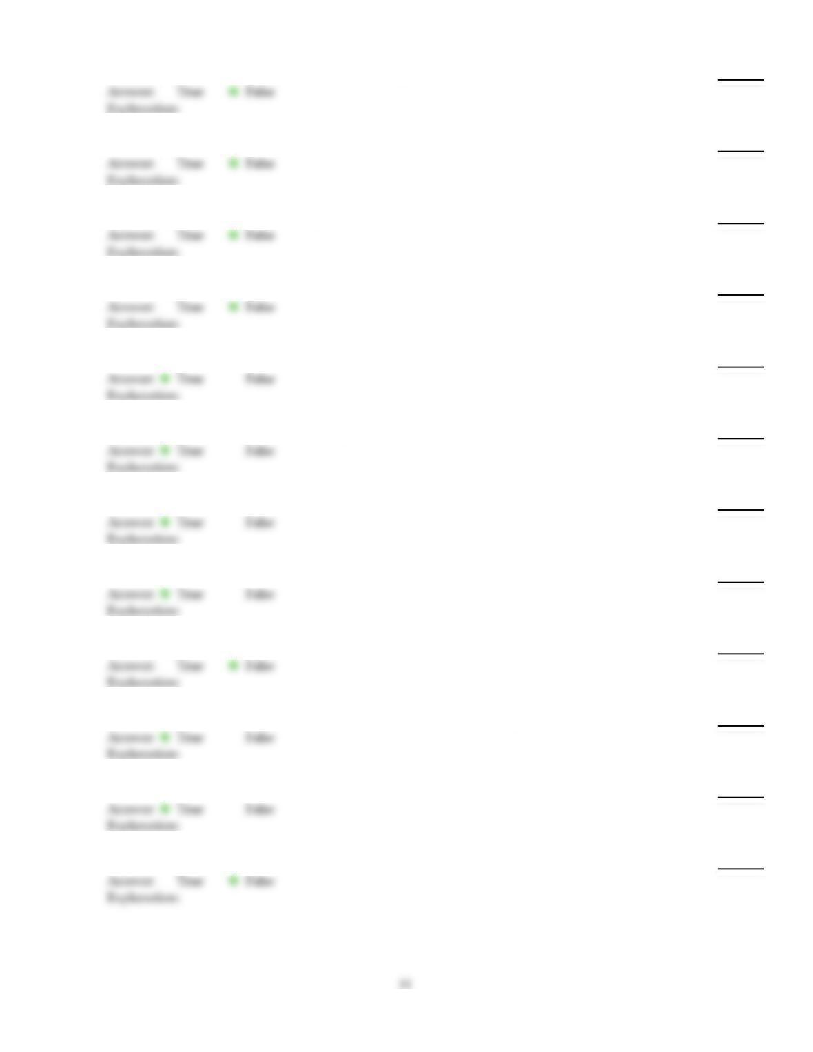
42)
The output of a NOR gate is HIGH only when all inputs are HIGH.
42)
43)
The output of a NOR gate is LOW only when all inputs are HIGH.
43)
44)
When the inputs to a 3–input AND gate are 001, the output is HIGH.
44)
45)
The output of an OR gate is LOW when at least one input is LOW.
45)
46)
When the inputs to a 3–input OR gate are 001, the output is HIGH.
46)
47)
The output of a 2–input Exclusive–NOR gate is HIGH when the inputs are equal, or identical.
47)
48)
The output of a NAND gate is LOW only when all inputs are HIGH.
48)
49)
The output of an OR gate is HIGH when at least one input is HIGH.
49)
50)
The output of a NAND gate is HIGH only when one or more inputs are HIGH.
50)
51)
A circle, or “bubble,” on a distinctive–shape logic symbol indicates a logic inversion.
51)
52)
A LOW input to an inverter produces a HIGH output.
52)
53)
The output of a 2–input Exclusive–OR gate is HIGH when the inputs are equal, or identical.
53)
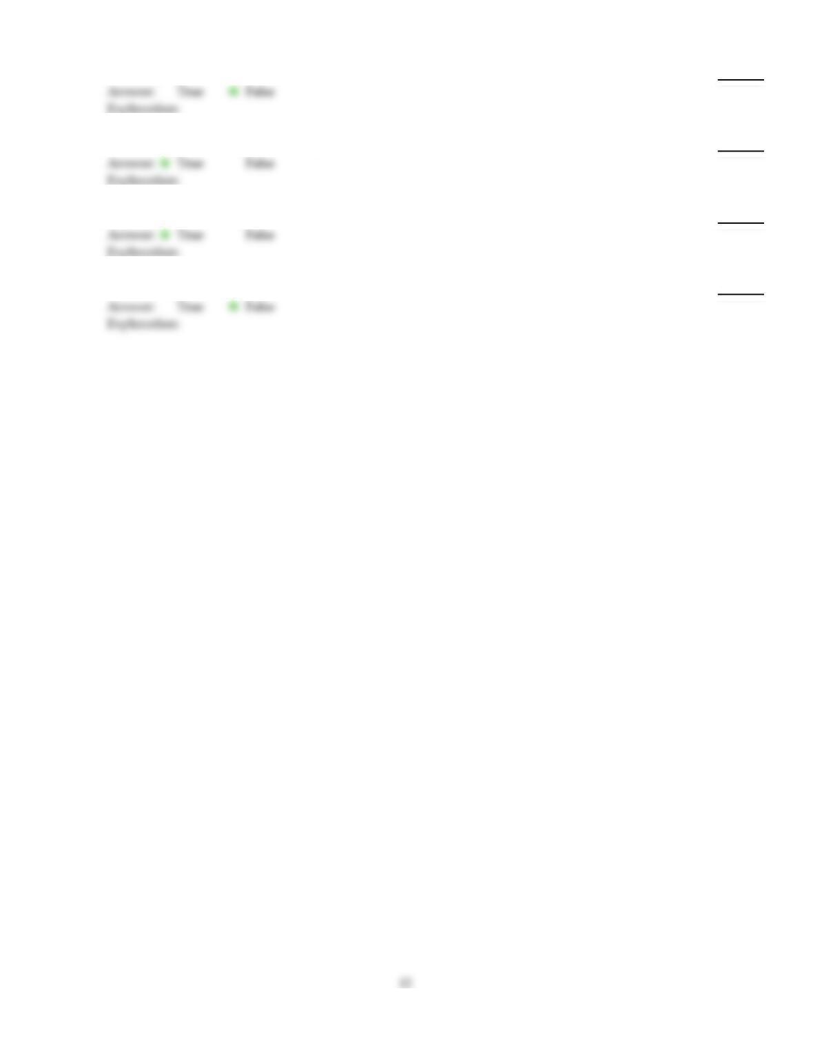
54)
The OR gate performs a function similar to series–connected switches.
54)
55)
When the inputs to a 3–input NOR gate are 001, the output is LOW.
55)
56)
The output of an AND gate is HIGH only when all inputs are HIGH.
56)
57)
The output of an AND gate is LOW only when all inputs are LOW.
57)
Answer Key
Testname: C3
41)
TRUE
42)
43)
44)
45)
46)
TRUE
47)
TRUE
48)
TRUE
49)
TRUE
50)
10)
11)
12)
13)
14)
15)
16)
17)
18)
19)
20)
21)
22)
23)
24)
25)
26)
27)
28)
29)
30)
31)
32)
33)
34)
35)
36)
37)
38)
39)
40)
Answer Key
Testname: C3