Exam
Name___________________________________
MULTIPLE CHOICE. Choose the one alternative that best completes the statement or answers the question.
1)
The HIGH logic level for a standard TTL output must be at least ________ V.
1)
A)
2.4
B)
5
C)
0.8
D)
2
2)
What is unique about 74SXX–series TTL devices?
2)
A)
The devices use Schottky transistors and diodes to prevent them from going into saturation;
this results in faster turn on and turn off times, which translates into higher frequency
operation.
B)
The gate transistors are silicon (S), and the gates therefore have lower values of leakage
current.
C)
The S denotes the fact that a single gate is present in the IC rather than the usual package of
2–6 gates.
D)
The S denotes a slow version of the device, which is a consequence of its higher power rating.
1
3)
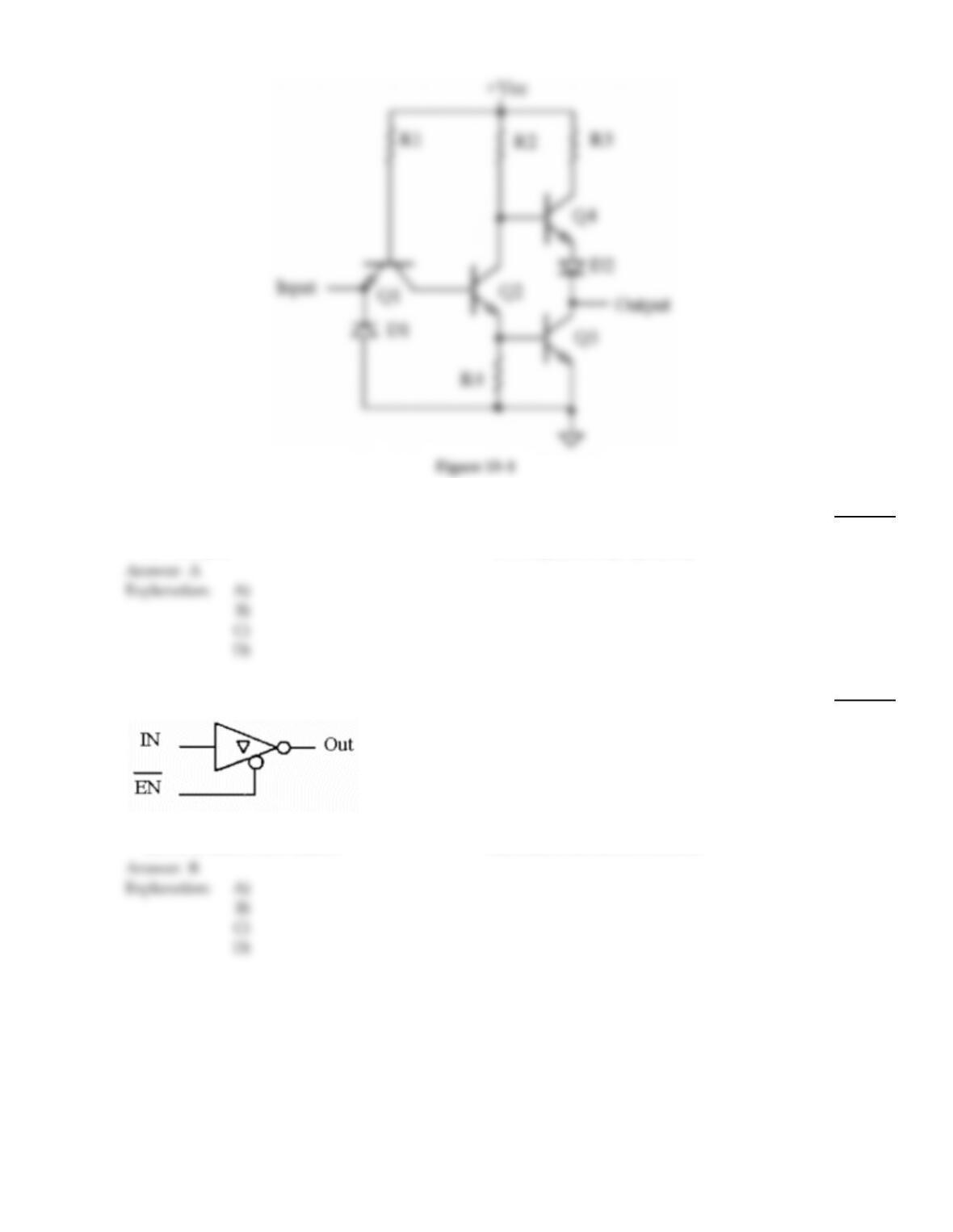
Refer to Figure 15–1. What is the output transistor configuration called?
3)
A)
Totem–Pole
B)
Quasi push–pull
C)
Push–pull
D)
Complementary–symmetry
4)
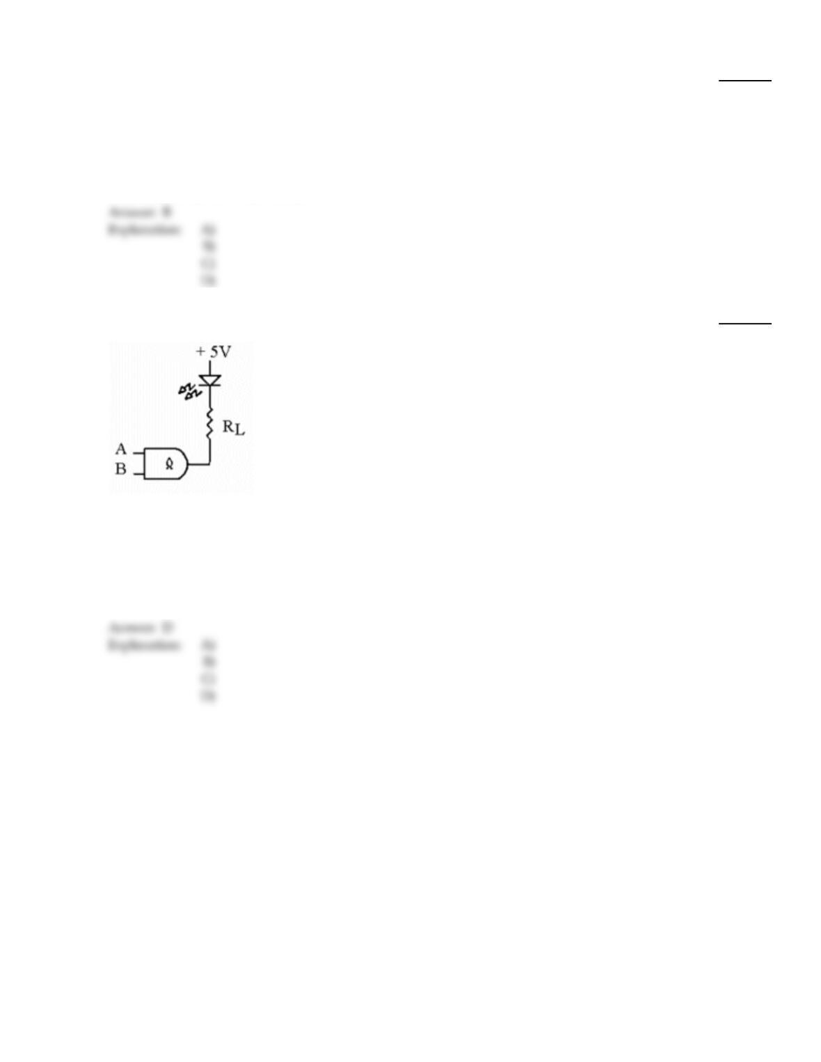
What type of circuit is represented below?
4)
A)
It is a programmable inverter.
B)
It is a tristate inverter.
C)
It is an active LOW buffer.
D)
None of the above is correct.
2
5)
PMOS and NMOS ________.
5)
A)
are enhancement type CMOS devices used to produce a series of high–speed logic known as
74HC
B)
represent MOSFET devices utilizing either p–channel or n–channel devices exclusively within
a given gate
C)
represent positive and negative MOS type devices which can be operated from differential
power supplies and are compatible with operational amplifiers
D)
none of the above are correct
6)
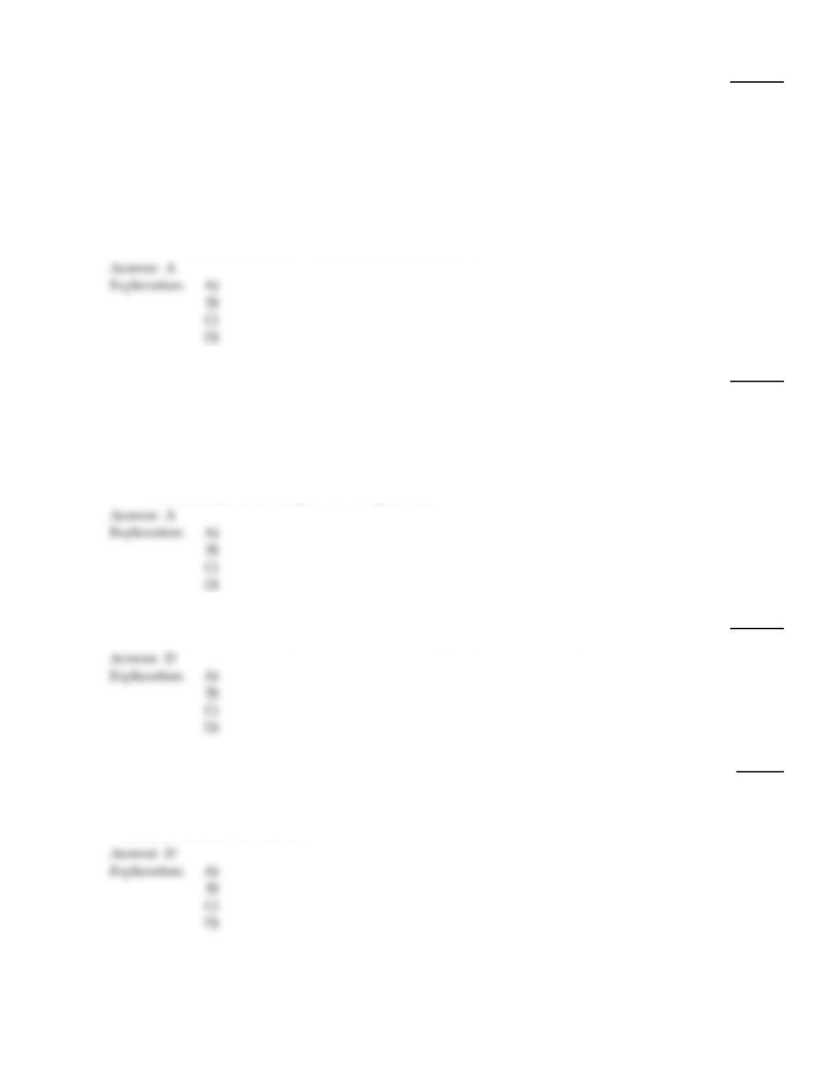
What type of device is shown below and what input levels are required to turn the LED off?
6)
A)
The device is a Schottky AND gate and requires only one low input to turn the LED off.
B)
The device is an open–collector AND gate and requires only one low input to turn the LED
off.
C)
The device is a Schottky open–collector AND gate and requires a low on both inputs to turn
the LED off.
D)
The device is an open–collector AND gate and requires both inputs to be HIGH in order to
turn the LED off.
3
7)
Why is the fanout of CMOS gates frequency dependent?
7)
A)
The input gates of the FETs are predominantly capacitive, and as the signal frequency
increases the capacitive loading also increases, thereby limiting the number of loads that may
be attached to the output of the driving gate.
B)
When the frequency reaches the critical value, the gate will only be capable of delivering 70%
of the normal output voltage and consequently the output power will be one–half of normal;
this defines the upper operating frequency.
C)
The higher the number of gates attached to the output, the more frequently they will have to
be serviced, thus reducing the frequency at which each will be serviced with an input signal.
D)
Each CMOS input gate has a specific propagation time and this limits the number of different
gates that can be connected to the output of a CMOS gate.
8)
What should be done to unused inputs on TTL gates?
8)
A)
Unused AND and NAND inputs should be tied to Vcc through a 1k–ohm resistor; unused OR
and NOR inputs should be grounded.
B)
All unused gates should be connected together and tied to Vcc through a 1k–ohm resistor.
C)
All unused inputs should be connected to an unused output; this will insure compatible
loading on both the unused inputs and unused outputs.
D)
They should be left disconnected so as not to produce a load on any of the other circuits and
to minimize power loading on the voltage source.
A
9)
Which of the following logic families has the highest noise margin?
9)
A)
CMOS
B)
TTL
C)
LS TTL
D)
HCMOS
D
10)
Which of the following statements apply to CMOS devices?
10)
A)
The devices should not be inserted into circuits with the power on.
B)
The devices should be stored and shipped in antistatic tubes or conductive foam.
C)
All tools, test equipment and metal workbenches should be tied to earth ground.
D)
All of the above are correct.
D
4
A
11)
When the output of a standard TTL gate is HIGH, it can ________.
11)
A)
sink 16mA of current from the attached input gates
B)
sink a maximum of 400–microamps from a maximum of 10 load gates
C)
source 400–microamps of current to a maximum of 10 attached gates
D)
source 16mA of current to a maximum of 10 attached gates
12)
Which of the logic families listed below allows the highest operating frequency?
12)
A)
HCMOS
B)
54S
C)
ECL
D)
74AS
13)
Which of the following logic families has the highest maximum clock frequency?
13)
A)
S–TTL
B)
HCMOS
C)
AS–TTL
D)
HS–TTL
14)
As more load gates are connected to a driving gate, the loading on the driving gate ________.
14)
A)
decreases
B)
increases
C)
serves as a current sink
D)
serves as a current source
15)
Which of the following logic families has the best noise immunity?
15)
A)
TTL
B)
HCMOS
C)
DTL
D)
ALS
5
16)
Which of the following accurately describes ECL?
16)
A)
ECL stands for electron–coupled logic; all of the devices used within the gates are N–type
transistors.
B)
ECL stands for energy–coupled logic; the input energy is amplified by the input transistors
and allows the device to deliver higher output currents.
C)
ECL stands for emitter–coupled logic; all of the emitters of the input transistors are connected
together and each transistor functions as an emitter follower.
D)
ECL stands for emitter–coupled logic; all of the inputs are coupled into the device through the
emitters of the input transistors.
17)
Totem–pole outputs ________.
17)
A)
can be connected in series when higher output voltages are required
B)
can be connected together to handle higher load currents and output voltages
C)
can be connected in parallel when higher output currents are required
D)
cannot be connected together because high currents can damage one or both of the transistors
if the outputs are in opposite states (one HIGH and one LOW)
18)
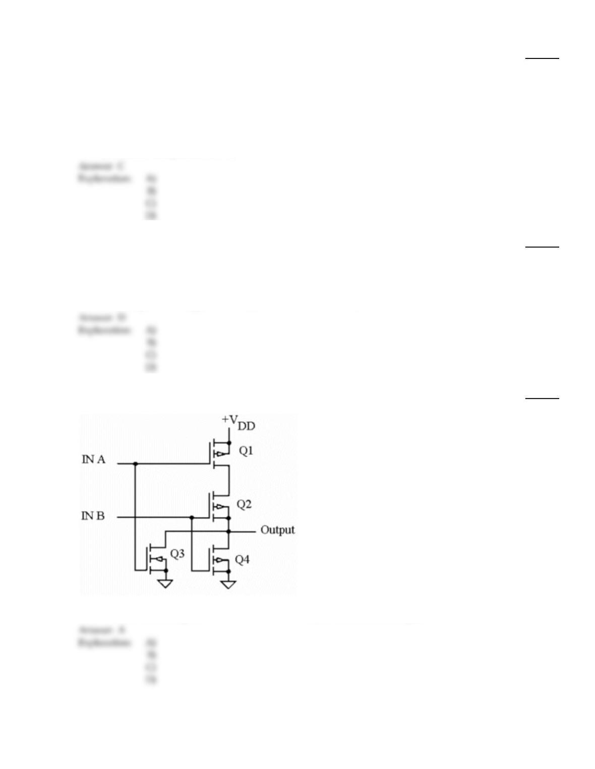
What type of logic circuit is shown below?
18)
A)
It is a CMOS NOR gate.
B)
It is a NMOS AND gate.
C)
It is a CMOS AND gate.
D)
It is a PMOS NAND gate.
6
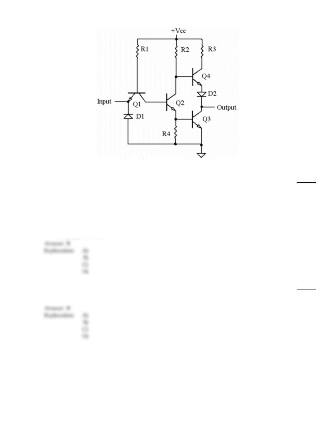
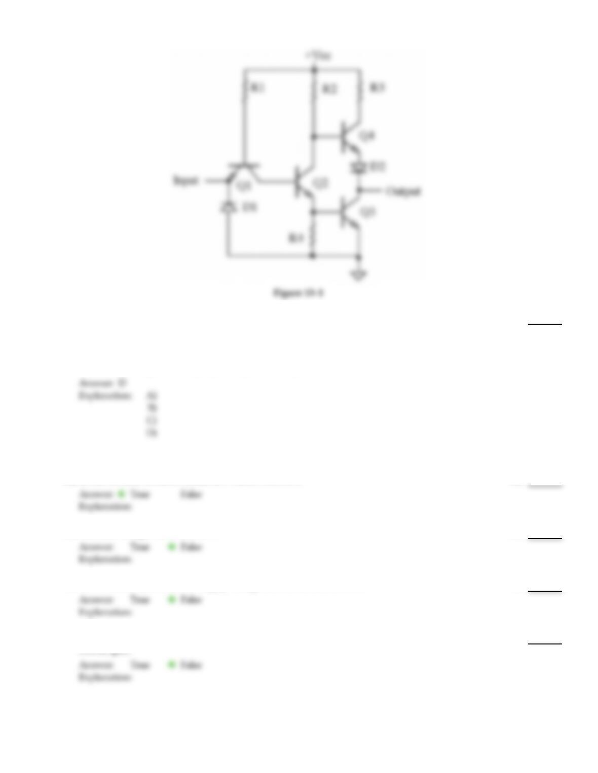
Figure 15–1
19)
What functions do D1 and D2 serve in Figure 15–1?
19)
A)
D1 and D2 are both steering diodes which are used to ensure that the input current is
correctly steered to the proper output terminal.
B)
D1 prevents negative spikes from damaging Q1, and D2 ensures that Q4 will be off when Q2
is on.
C)
D1 clamps the input of Q1 to prevent saturation, and D2 prevents reverse voltage spikes from
damaging Q4.
D)
D1 provides a return path for the emitter current of Q1, and D2 prevents reverse voltage from
being applied to Q3.
20)
Which of the following will not normally be found on a data sheet?
20)
A)
Maximum LOW level output voltage
B)
Minimum LOW level output voltage
C)
Minimum HIGH level output voltage
D)
Maximum HIGH level input current
7
21)
Propagation delay is important because ________.
21)
A)
all the gates in a system must have the same propagation times in order to be compatible
B)
it limits the maximum operating frequency of a gate
C)
it is a measure of how long the clock must be applied to the gate before it will make the
required decision
D)
the logic gates must be given a short break during each clock cycle or else they will overheat
22)
Which of the following summarizes the important features of ECL?
22)
A)
Good noise immunity, negative logic, high frequency capability, low power dissipation and
short propagation time.
B)
Poor noise immunity, positive supply voltage operation, good low frequency operation, and
low power.
C)
Slow propagation time, high frequency response, low power consumption, and high output
voltage swings.
D)
Low noise margin, low output voltage swing, negative voltage operation, fast, and high
power consumption.
23)
Which of the following logic families has the shortest propagation delay?
23)
A)
HCMOS
B)
HS–TTL
C)
S–TTL
D)
AS–TTL
24)
What are the major differences between the 5400 and 7400 series of ICS?
24)
A)
The 5400 series are military grade and allow for a wider range of supply voltage and
temperatures.
B)
The 7400 series was originally developed by Texas Instruments; the 5400 series was brought
out by National Semiconductors after TI’s patents expired, as a second supply source.
C)
The 5400 series are military grade and require tighter supply voltages and temperatures.
D)
The 7400 series are an improvement over the original 5400s.
8
25)
The LOW logic level for standard TTL input cannot exceed ________.
25)
A)
0.0V.
B)
5V.
C)
0.4V.
D)
0.8V.
26)
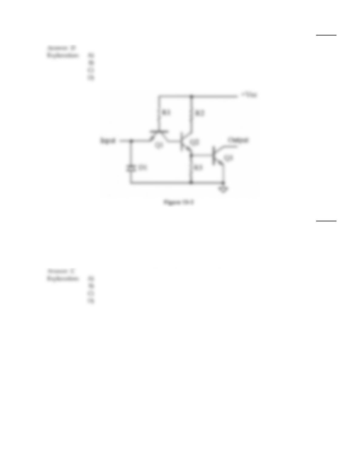
What type of circuit is shown in Figure 15–2, and how is the output ordinarily connected?
26)
A)
It represents an active–LOW inverter and is used in negative logic systems.
B)
It is an open–collector gate and is used to drive loads that cannot be connected directly to Vcc
due to high noise levels.
C)
It is an open–collector gate. An external load must be connected between the output terminal
and an appropriate supply voltage terminal.
D)
Any of the above could be correct, depending on the specific application involved.
9
27)
Refer to Figure 15–1. Which of the following describes the operation of the circuit?
27)
A)
A LOW input turns Q1 and Q4 off, Q2 and Q3 are on.
B)
A LOW input turns Q1 and Q3 on; Q2 and Q4 are off.
C)
A HIGH input turns Q1, Q2 and Q4 on; and Q3 is off.
D)
A HIGH input turns Q1, Q2 and Q3 off, and Q4 on.
TRUE/FALSE. Write ‘T’ if the statement is true and ‘F’ if the statement is false.
28)
CMOS circuits utilize enhancement–mode MOSFETs.
28)
29)
The noise margin for TTL is 0.8V.
29)
30)
The nominal value of the dc supply voltage for TTL devices is +3.3V.
30)
31)
NMOS devices use MOSFETs to implement the full range of logic functions using the universal
NAND gate.
31)
10
32)
The average power dissipation for TTL can be calculated using PD= VCCICC.
32)
33)
The fanout of CMOS gates is frequency dependent.
33)
34)
ECL gates are noted for their high frequency capability and low–amplitude output voltage.
34)
35)
Due to the extremely low power requirements of CMOS logic circuits, any number of CMOS and
TTL gates can be interconnected.
35)
36)
The data sheet for the 74 series of TTL ICs shows that VCC has a range of 4.5 V to 5.5 V.
36)
37)
The term open–drain means that the drain terminal of the output transistor is not internally
connected to the supply voltage.
37)
38)
Most TTL gates contain a totem–pole output circuit.
38)
39)
Propagation delay time is the time delay between an input signal causing an output signal.
39)
40)
The TTL HIGH level source current is higher than the LOW level sinking current.
40)
11
Answer Key
Testname: C15
12