Exam
Name___________________________________
MULTIPLE CHOICE. Choose the one alternative that best completes the statement or answers the question.
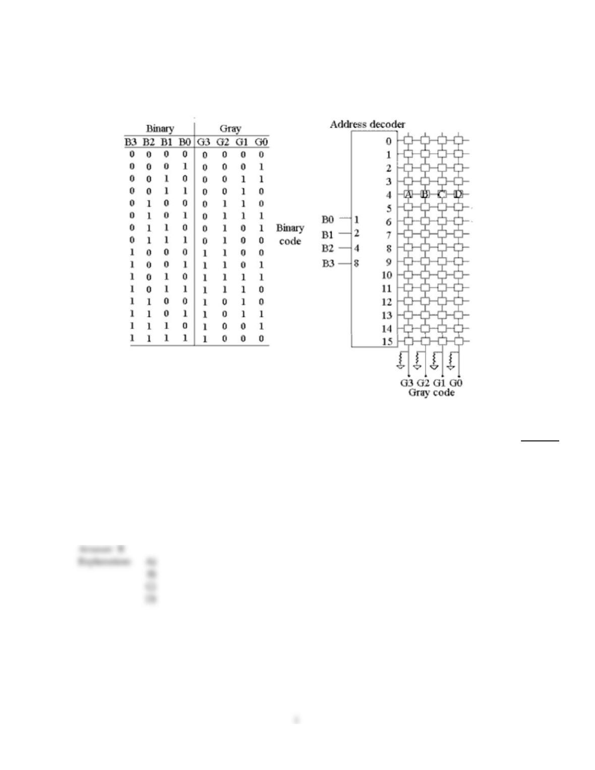
Figure 11–2
1)
Refer to Figure 11–2. The Binary–to–Gray converter is not working correctly. How could it be
checked?
1)
A)
Reverse the operation of the converter by applying the Gray code to the G terminals and
check for proper output on the B terminals.
B)
Step the inputs through their full range and check the outputs with a multi–channel scope or
logic analyzer.
C)
Measure the inputs and outputs with an ohmmeter to see if any of them are shorted.
D)
Any of the above methods could be tried, depending on the particular type of ROM being
used.
2)
What is RAM?
2)
A)
It is memory that is used for short–term temporary data storage within the computer.
B)
It is memory that can be reached by any sub–system within a computer, and at any time.
C)
It is the first level of memory used by the computer in all of its operations.
D)
It is memory that can be used and then automatically reset, or cleared, after being read from
or written to.
3)
Which of the following best describes EPROMs?
3)
A)
EPROMs can be erased by UV light.
B)
EPROMs can be erased by shorting all inputs to ground.
C)
EPROMs can only be programmed once.
D)
All of the above are correct.
A
4)
The checksum method is used to test ________.
4)
A)
RAM
B)
EEPROM
C)
ROM
D)
FPLA
C
5)
A DRAM has a RAS and a CAS because ________.
5)
A)
the RAS determines the operation mode and the CAS enables the tri–state outputs
B)
the RAS latches in the address and the CAS latches in data
C)
the address lines are multiplexed to reduce pin count
D)
none of the above
C
A
6)
Which of the following faults will the checkerboard pattern detect in RAM?
6)
A)
Dynamically introduced errors between cells
B)
Short between adjacent cells
C)
Ability to store both 0s and 1s
D)
All of the above.
7)
Eight bits of digital data are normally referred to as a ________.
7)
A)
cell
B)
byte
C)
group
D)
word
8)
A DIMM ________.
8)
A)
has contact pins on both sides of the module for larger data paths
B)
has less memory than the newer SIMM modules
C)
has contact pins on only one side of the module
D)
is available in 30–pin or 72–pin packages
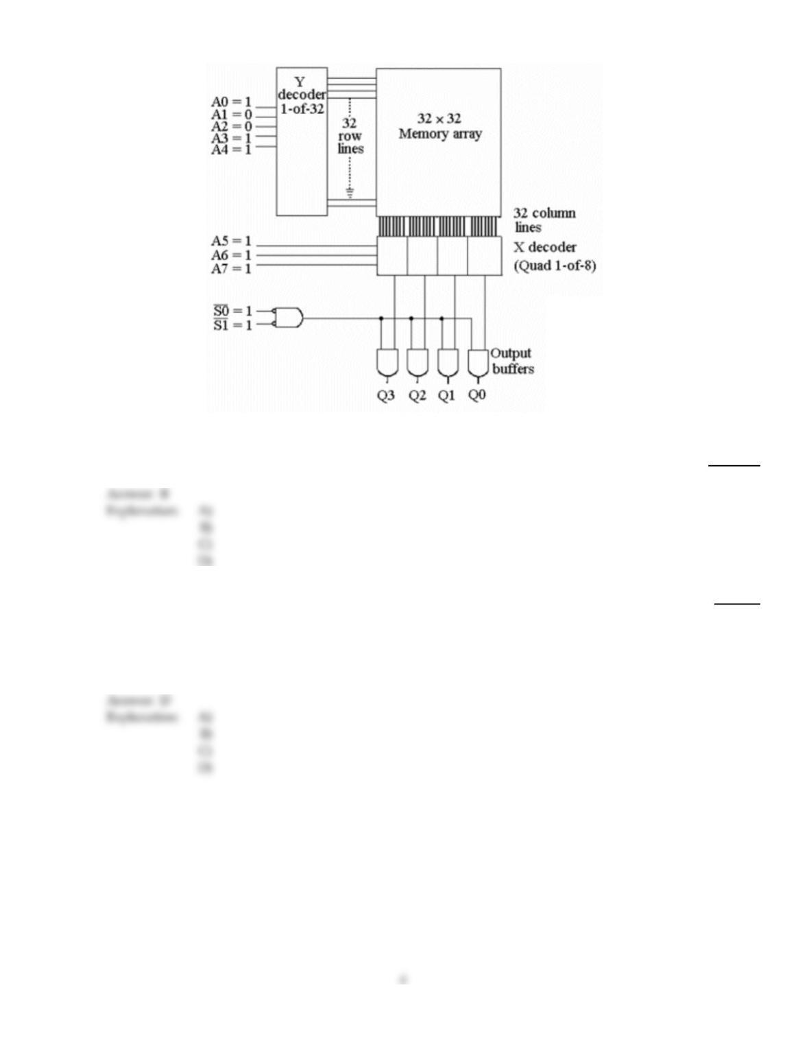
Figure 11–3
9)
For the circuit in Figure 11–3, the value at the Q3 – Q0 outputs will be ________.
9)
A)
1111
B)
0000
C)
1001
D)
1024
10)
What is the major difference between SRAM and DRAM?
10)
A)
SRAMs can hold data via a static charge, even with power off.
B)
The only difference is the terminal from which the data is removed: from the FET Drain or
Source.
C)
Dynamic RAMs are always active; Static RAMs must rest between data read/write cycles.
D)
DRAMs must be periodically refreshed.
11)
What do the letters PROM stand for?
11)
A)
Programmed Random Only Memory
B)
Programmed Read Only Memory
C)
Programmed Registers On Microprocessors
D)
Programmable Read Only Memory
12)
Which of the following is one of the basic characteristics of DRAMs?
12)
A)
DRAMs have a broader “dynamic” storage range than other types of memories.
B)
DRAMs must be periodically refreshed in order to retain data.
C)
DRAMs are simpler devices than other type memories.
D)
DRAMs must have a constantly changing input.
13)
The difference between RAM and ROM is ________.
13)
A)
RAM has a read/write signal and ROM doesn’t
B)
RAM loses data when the power is removed and ROM doesn’t
C)
RAM has random address access and ROM uses sequential address access
D)
all of the above
E)
A and B only
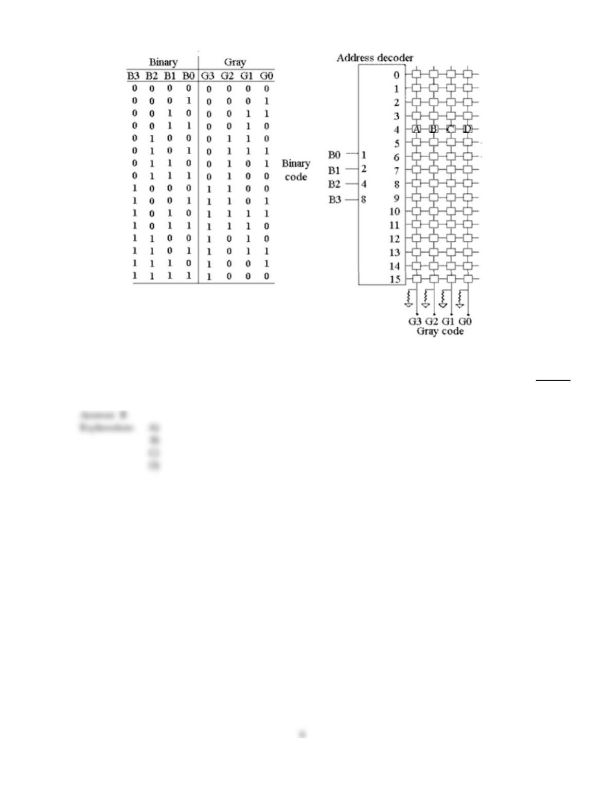
Figure 11–2
14)
Refer to Figure 11–2. What address line or lines are HIGH if it is desired to input a decimal 10 into
the code converter (address decoder) and what is the resulting Gray code output value?
14)
A)
10, 1010
B)
2 and 8, 1111
C)
8 and 2, 1010
D)
10, 1111
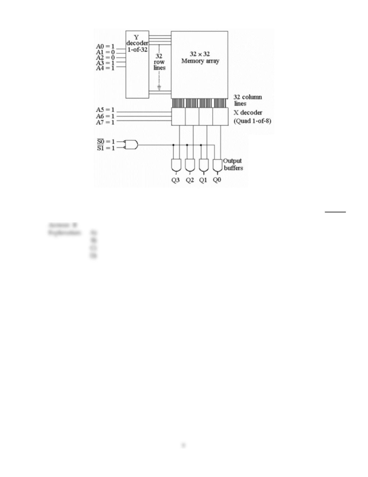
Figure 11–3
15)
For the circuit of Figure 11–3, how many bits are contained in the output data word?
15)
A)
3
B)
4
C)
32
D)
8
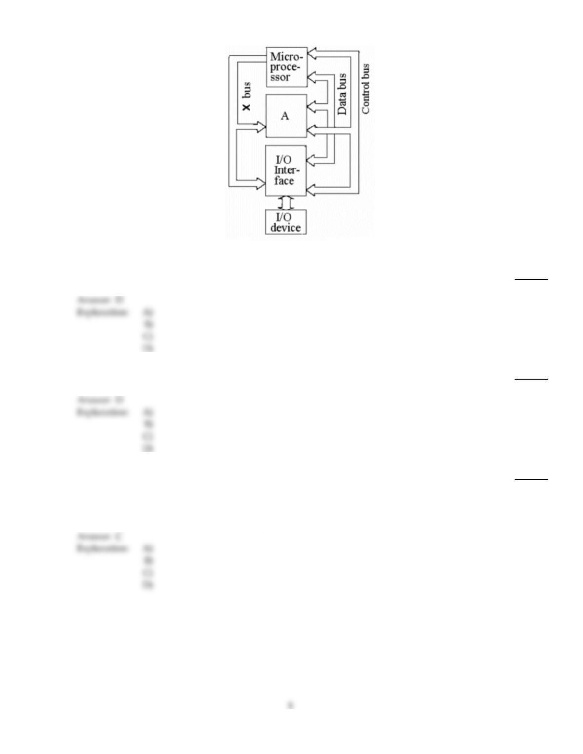
Figure 11–1
16)
The point identified as the “X bus” in Figure 11–1 is the ________ bus.
16)
A)
memory
B)
I/O
C)
supply
D)
address
17)
Which type of ROM can be electrically erased?
17)
A)
DRAM
B)
SRAM
C)
EPROM
D)
EEPROM
18)
Which of the following describes the action of storing a bit of data in a mask ROM?
18)
A)
A 0 is stored by connecting the gate of a MOS cell to the address line.
B)
A 1 is stored in a bipolar cell by opening the base connection to the address line.
C)
A 1 is stored by connecting the gate of a MOS cell to the address line.
D)
A 0 is stored in a bipolar cell by shorting the base connection to the address line.
19)
The remote servers in a cloud storage system are referred to as ________.
19)
A)
servers.
B)
nodes
C)
clouds
D)
users
20)
The arrangement of tracks and sectors on a disk is known as the ________.
20)
A)
performance
B)
physical address
C)
partition
D)
format
21)
The checkerboard pattern test is used to test ________.
21)
A)
FPLA
B)
ROM
C)
EEPROM
D)
RAM
22)
Which of the following is correct for the circuit shown in Figure 11–4?
22)
A)
The number 5 is being written to the memory at address location 203.
B)
The chip has not been enabled, since the EN terminal is 0; therefore, nothing will be written to
the chip and the output is tri–stated.
C)
The read/write line is LOW; therefore decimal 5 is being stored at memory location 211.
D)
Decimal 10 is being written into memory location 211.
Figure 11–3
23)
What memory location is being addressed in Figure 11–3?
23)
A)
5
B)
10111
C)
249
D)
157
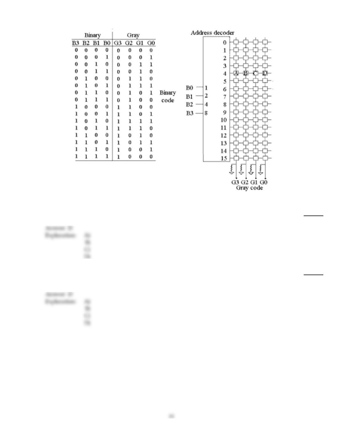
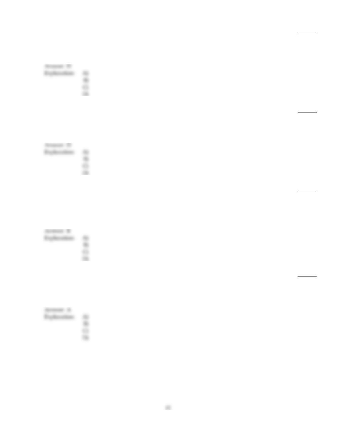
Figure 11–2
24)
What are the values of A, B, C and D in Figure 11–2?
24)
A)
0 1 1 1
B)
0 1 0 0
C)
0 0 1 0
D)
0 1 1 0
25)
Which of the following methods is not normally associated with producing PROMs?
25)
A)
Metal links
B)
Shorted junctions
C)
Silicon links
D)
spst switches
26)
ROM access time is defined as ________.
26)
A)
being the difference between the READ and WRITE times
B)
how long it takes to program the ROM chip
C)
the time required to activate the address lines after the ENABLE line is at a valid level
D)
the time it takes to get valid output data after a valid address is applied
27)
A FIFO ________.
27)
A)
allows data to be clocked in and out at different clock rates
B)
can be used to smooth out bursts of data into a continuous stream
C)
outputs data in the same order that it was input
D)
all of the above
28)
A 64–Mbyte SIMM is installed into a system, but when a memory test is executed, the SIMM is
detected as a 32–Mbyte device. What is a possible cause?
28)
A)
The voltage on the memory module is incorrect.
B)
The address decoder on the SIMM is faulty.
C)
The most significant address line is stuck high or low.
D)
The memory module was not installed properly.
29)
The hard drive latency period is defined as ________.
29)
A)
the time that it takes for the desired sector to spin under the head once the head is positioned.
B)
the time that it takes a hard drive to switch from read mode to write mode.
C)
the time that it takes a hard drive to spin up from 0 rpm to 3600 rpm.
D)
the time that it takes to spin down a hard drive for power off.
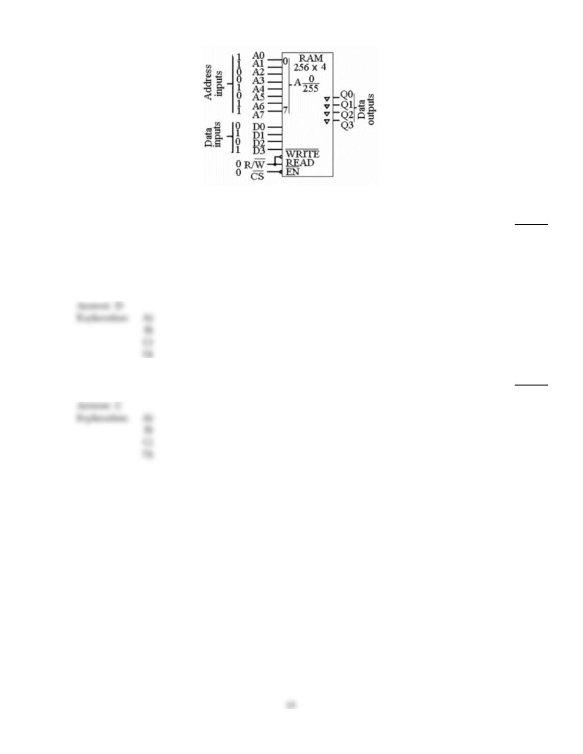
Figure 11–4
30)
What is the significance of the inverted triangles on the outputs of the device in Figure 11–4?
30)
A)
It means that the outputs will only be active if a change has occurred at that memory location
since the last read/write cycle.
B)
They represent inverters and mean that the outputs are active–LOW.
C)
They represent buffers and mean that the outputs can drive 40 TTL loads, instead of the
normal 10.
D)
The IC has tri–state outputs.
31)
Which of the following is not a type of memory?
31)
A)
RAM
B)
EEPROM
C)
FPROM
D)
ROM
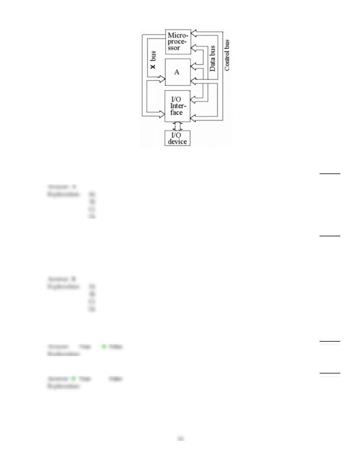
Figure 11–1
32)
The block identified as A in Figure 11–1 is the ________.
32)
A)
memory
B)
controller
C)
addresser
D)
clock
33)
How can UV–erasable PROMs be recognized?
33)
A)
They will have a small violet dot next to the #l pin.
B)
By a small window on the chip
C)
They can be identified by the fact that their part number always starts with a “U”, such as in
U12.
D)
They are not readily identifiable, since they must always be kept under a small cover.
TRUE/FALSE. Write ‘T’ if the statement is true and ‘F’ if the statement is false.
34)
The term “cloud storage” refers to a specific type of memory within your computer or pad.
34)
35)
A flash drive obtains power from the computer to which it is attached.
35)
36)
One of the advantages of DRAMs is their ability to store data without the need for periodically
refreshing the memory contents.
36)
37)
Fusible link PROMs are programmed removing the desired fuse links using a highly focused beam
of light.
37)
38)
The term “storage” refers to CD–ROMs, floppy disks, and hard disks.
38)
39)
ROMs are used to store data that is not intended to be changed easily.
39)
40)
RAMs must have a READ/WRITE input, in addition to one or more DATA inputs.
40)
41)
RAM stands for Readily Accessible Memory.
41)
42)
Each memory cell can store one byte of information.
42)
43)
The term “Blu–Ray” comes from the fact that the disc is read using a blue laser (as opposed to a red
laser).
43)
44)
A bank is a section of memory that is contained within a single chip.
44)
45)
Due to their ability to be easily erased and reused, magnetic memory devices are widely used for
RAM.
45)
46)
A rank is a memory section that takes priority over other memory sections.
46)
47)
DIMMS generally contain DDR SDRAM memory chips.
47)
48)
Flash drives use USB B–type connectors.
48)
49)
Main computer memory is usually DRAM because of high density and low cost while cache
memory is usually SRAM because of high speed.
49)
50)
Referring to a DDR SDRAM, DDR stands for Dual Data Retrieval.
50)
51)
EEPROMS can be electrically erased and reused.
51)
Answer Key
Testname: C11

Answer Key
Testname: C11