Exam
Name___________________________________
MULTIPLE CHOICE. Choose the one alternative that best completes the statement or answers the question.
1)
Which one of the circuits listed is made up of flip–flops?
1)
A)
A converter
B)
A multiplexer
C)
A register
D)
A comparator
2)
Item (4) of the nonideal pulse in Figure 1–2 represents the waveform ________.
2)
A)
amplitude
B)
rise time
C)
fall time
D)
pulse width
3)
A circuit that converts an digital signal to an analog waveform is commonly called a(n) ________.
3)
A)
PLD
B)
CAD
C)
ADC
D)
DAC
4)
The approximate duty cycle for the digital waveform below is ________.
4)
A)
30%
B)
50%
C)
80%
D)
20%
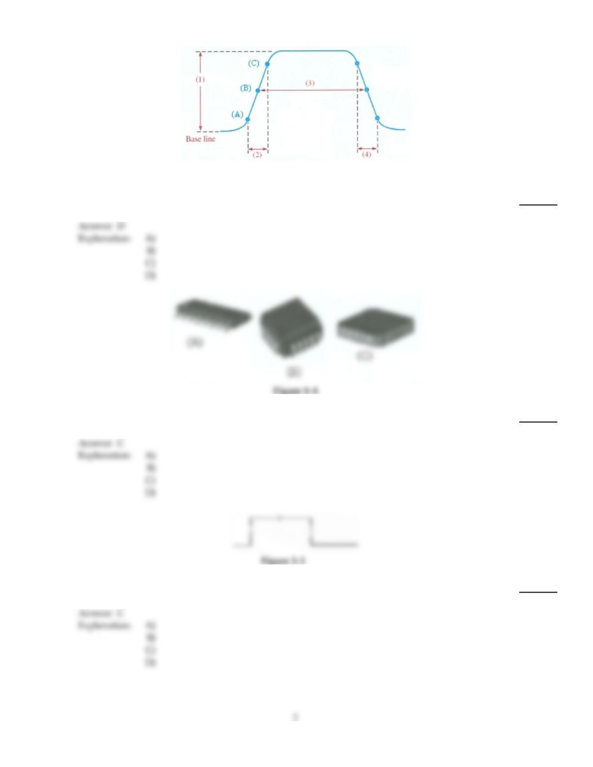
Figure 1–2
5)
Item (3) of the nonideal pulse in Figure 1–2 represents the waveform ________.
5)
A)
amplitude
B)
rise time
C)
fall time
D)
pulse width
6)
The package style in Figure 1–4(C) is a(n) ________.
6)
A)
SOIC
B)
PLCC
C)
LCCC
D)
FP
7)
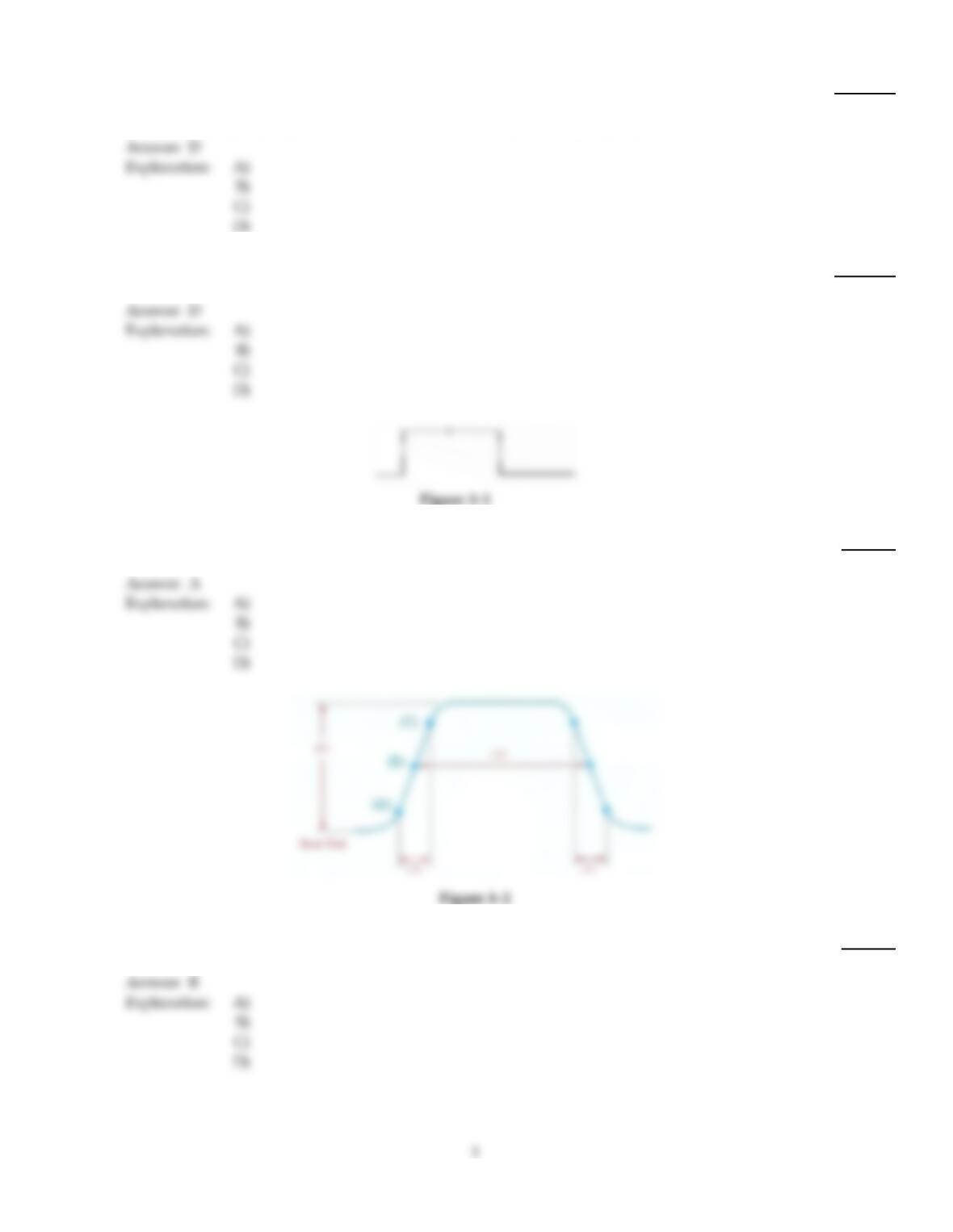
Which edge in Figure 1–1 is the trailing edge?
7)
A)
1
B)
2
C)
3
D)
Both 1 and 3
8)
On a positive–going pulse, the leading edge is the ________.
8)
A)
HIGH–to–LOW transition
B)
falling edge
C)
negative–going edge
D)
positive–going edge
9)
Which circuit converts data from serial form to parallel form?
9)
A)
Multiplexer
B)
Encoder
C)
Comparator
D)
Demultiplexer
10)
Which edge in Figure 1–1 is the leading edge?
10)
A)
1
B)
2
C)
3
D)
Both 1 and 3
11)
Item (2) of the nonideal pulse in Figure 1–2 represents the waveform ________.
11)
A)
amplitude
B)
rise time
C)
fall time
D)
pulse width
12)
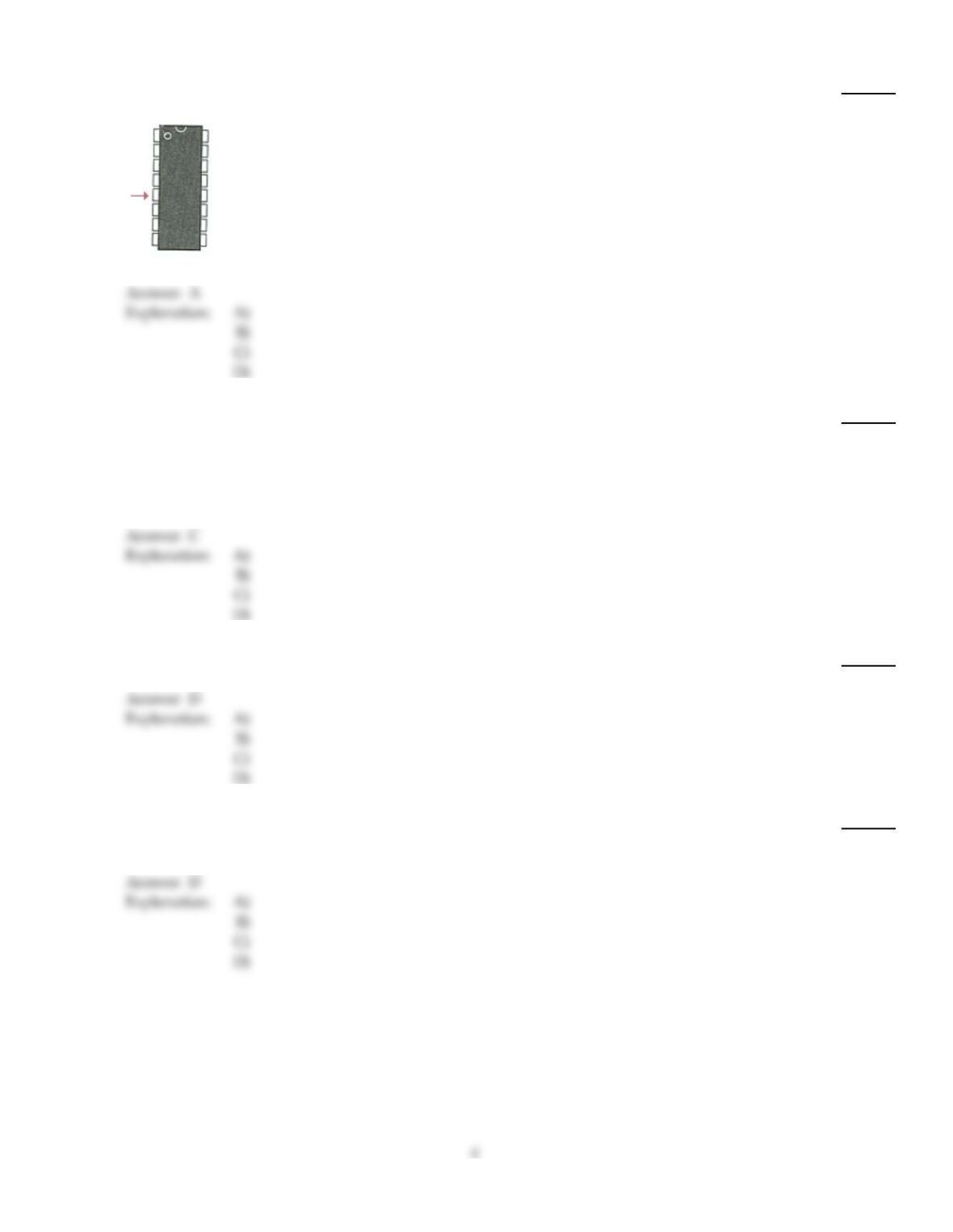
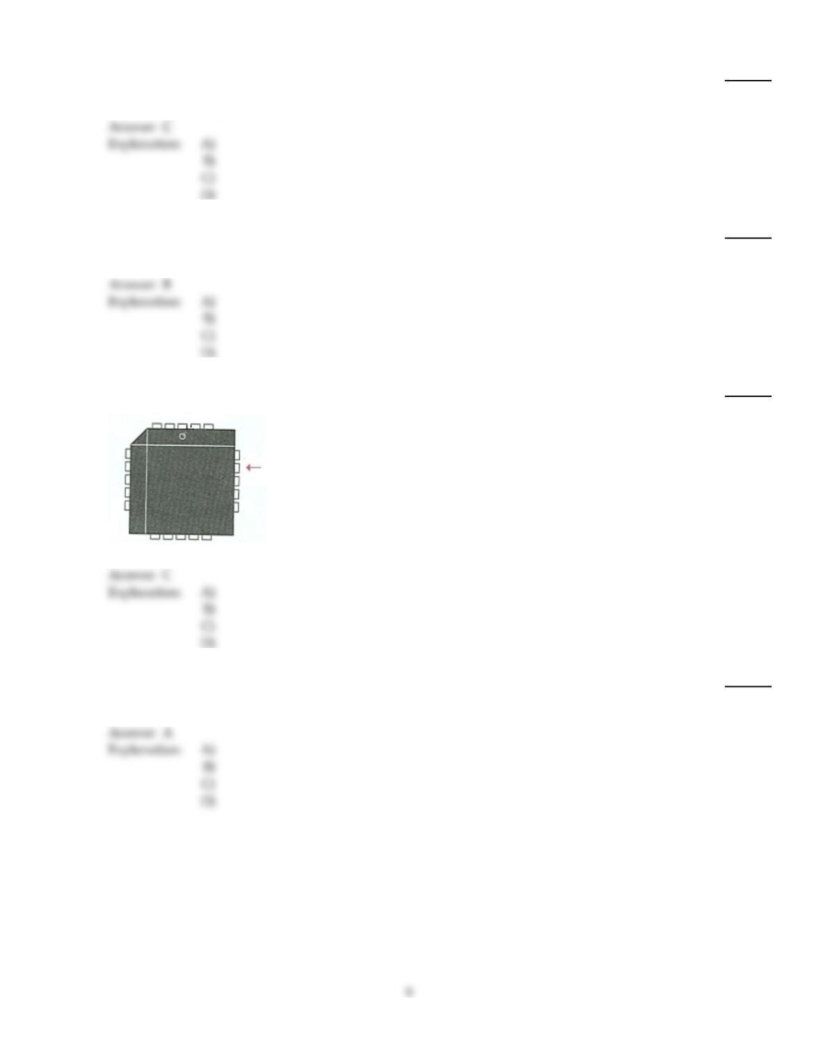
The arrow in the figure below points to pin number ________.
12)
A)
5
B)
13
C)
4
D)
12
13)
An oscilloscope display indicates that the period of a digital waveform is 40 µs. What is frequency
of this waveform?
13)
A)
40 MHz
B)
2.5 kHz
C)
25 kHz
D)
The frequency cannot be determined using the information provided.
14)
The final step in the PLD programming process is ________.
14)
A)
design entry
B)
compilation
C)
synthesis
D)
download
15)
On a positive–logic pulse, the trailing edge is the ________.
15)
A)
positive–going edge
B)
rising edge
C)
LOW–to–HIGH transition
D)
falling edge
16)
Which of the following is an example of a mechatronics system?
16)
A)
A surgical laser
B)
A laptop computer
C)
An industrial robot
D)
None of the above
17)
The time from one leading edge on a digital waveform to the next is the waveform ________.
17)
A)
fall time
B)
rise time
C)
pulse width
D)
period
18)
On a digital waveform, the transition time from a LOW level to a HIGH level is called ________.
18)
A)
fall time
B)
pulse width
C)
period
D)
rise time
19)
Which circuit converts information into a specific coded form?
19)
A)
Comparator
B)
Encoder
C)
Decoder
D)
Multiplexer
20)
Which IC package style has no leads?
20)
A)
SOIC
B)
LCCC
C)
PLCC
D)
All must have leads.
21)
A circuit that converts an analog waveform to a digital signal is commonly called a(n) ________.
21)
A)
ADC
B)
CAD
C)
DAC
D)
PLD
22)
The transition times for an ideal digital pulse are ________.
22)
A)
measured between 0 and 90% of the amplitude
B)
measured between 10% to 90% of the amplitude
C)
infinite
D)
zero
23)
Which circuit converts coded information into a noncoded form?
23)
A)
Comparator
B)
Encoder
C)
Decoder
D)
Multiplexer
24)
The output from an OR gate is LOW ________.
24)
A)
whenever any input is HIGH
B)
only when all inputs are LOW
C)
only when all inputs are HIGH
D)
none of the above
25)
Which one of the following is not a surface–mount IC package?
25)
A)
SOIC
B)
FP
C)
DIP
D)
PLCC
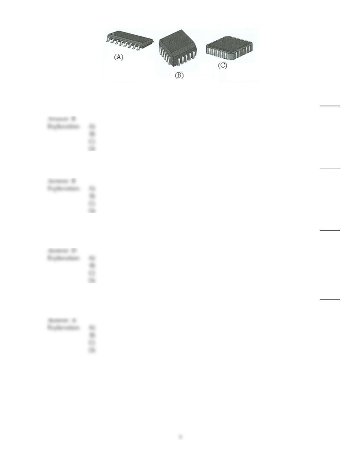
Figure 1–4
26)
The package style in Figure 1–4(B) is a(n) ________.
26)
A)
SOIC
B)
PLCC
C)
LCCC
D)
FP
27)
Which one of the following is not a binary arithmetic function?
27)
A)
Subtraction
B)
Multiplexing
C)
Division
D)
Addition
28)
A periodic digital waveform ________.
28)
A)
has a duty cycle
B)
repeats itself at a fixed interval
C)
has both a HIGH and LOW levels
D)
all of the above
29)
Two kinds of data selectors are ________ and ________.
29)
A)
multiplexers, demultiplexers
B)
comparators, registers
C)
adders, subtractors
D)
encoders, decoders
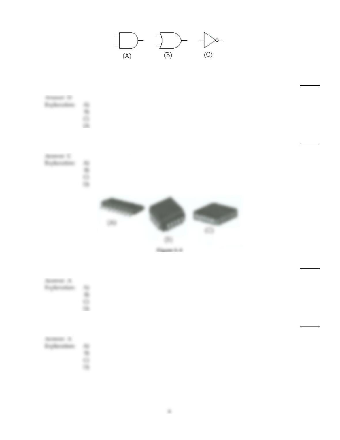
Figure 1–3
30)
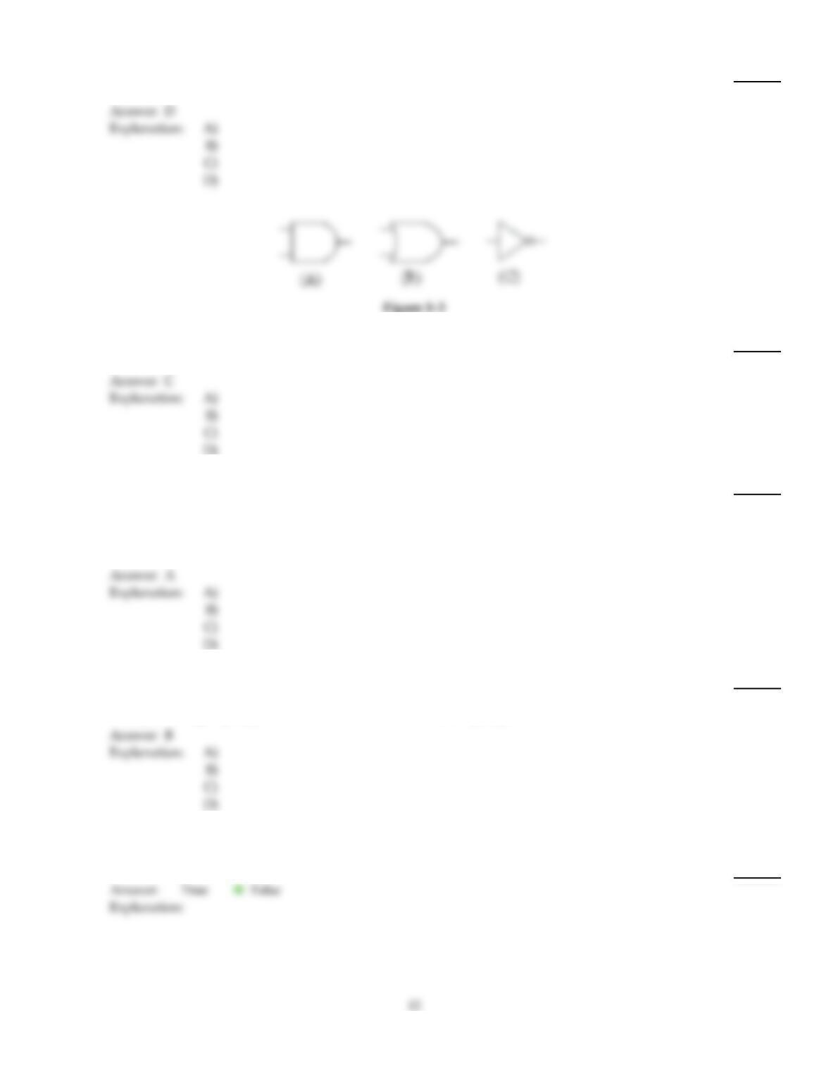
The symbol in Figure 1–3(C) represents the ________ function.
30)
A)
OR
B)
AND
C)
XOR
D)
NOT
31)
The netlist is generated during the ________ phase of the PLD programming process.
31)
A)
design entry
B)
compilation
C)
synthesis
D)
download
32)
The package style in Figure 1–4(A) is a(n) ________.
32)
A)
SOIC
B)
PLCC
C)
LCCC
D)
FP
33)
The first step in the PLD programming process is ________.
33)
A)
design entry
B)
compilation
C)
synthesis
D)
download
34)
On a negative–logic pulse, the trailing edge is the ________.
34)
A)
falling edge
B)
negative–going edge
C)
positive–going edge
D)
HIGH–to–LOW transition
35)
When data is set along a single conductor, it is referred to as ________.
35)
A)
parallel data
B)
serial data
C)
simultaneous data
D)
none of these
36)
The arrow in the figure below points to pin ________.
36)
A)
16
B)
4
C)
17
D)
5
37)
The output from an OR gate is HIGH ________.
37)
A)
when at least one input is HIGH
B)
only when all inputs are HIGH
C)
only when all inputs are LOW
D)
none of the above
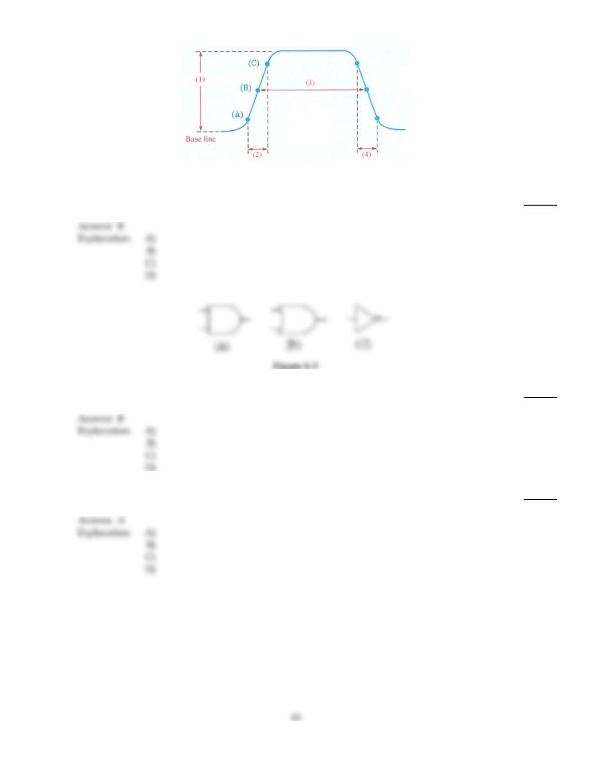
Figure 1–2
38)
Item (1) of the nonideal pulse in Figure 1–2 represents the waveform ________.
38)
A)
period
B)
amplitude
C)
transition time
D)
pulse width
39)
The symbol in Figure 1–3(B) represents the ________ function.
39)
A)
NON
B)
OR
C)
AND
D)
XOR
40)
Which circuit creates an output that indicates whether or not the input values are equal?
40)
A)
Comparator
B)
Encoder
C)
Decoder
D)
Multiplexer
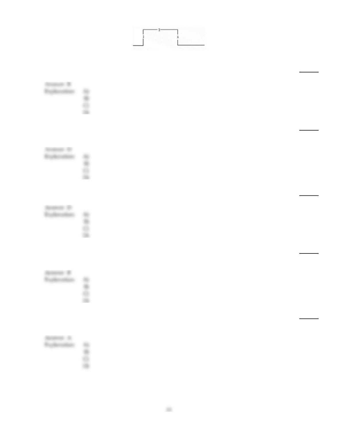
Figure 1–1
41)
The time between transition 1 and transition 3 in Figure 1–1 is the ________.
41)
A)
frequency
B)
pulse width
C)
period
D)
amplitude
42)
On a negative–going pulse, ________.
42)
A)
HIGH = 1 and LOW = 0
B)
HIGH = 0 and LOW = –1
C)
LOW = –1 and HIGH = 1
D)
HIGH = 0 and LOW = 1
43)
On a digital waveform, the transition time from a HIGH level to a LOW level is called ________.
43)
A)
period
B)
rise time
C)
pulse width
D)
fall time
44)
The output from an AND gate is LOW ________.
44)
A)
only when all inputs are LOW
B)
when at least one input is LOW
C)
only when all inputs are HIGH
D)
none of the above
45)
Of the circuits listed, the one that is most likely to be found in a CD player is a(n) ________.
45)
A)
digital–to–analog converter
B)
programmable logic device
C)
SPLD
D)
analog–to–digital converter
46)
What is the duty cycle of a digital waveform with a pulse width of 10 ms a period of 90 ms?
46)
A)
90%
B)
10%
C)
9%
D)
11.1%
47)
The symbol in Figure 1–3(A) represents the ________ function.
47)
A)
NOT
B)
OR
C)
AND
D)
AND/OR
48)
The output from an AND gate is HIGH when ________.
48)
A)
all inputs are HIGH
B)
one input is HIGH and the remaining inputs are LOW
C)
one input is LOW and the remaining inputs are HIGH
D)
all inputs are LOW
49)
On a negative–going pulse, the leading edge is the ________.
49)
A)
LOW–to–HIGH transition
B)
negative–going edge
C)
positive–going edge
D)
rising edge
TRUE/FALSE. Write ‘T’ if the statement is true and ‘F’ if the statement is false.
50)
Clock signals carry pieces of information such as letters and numbers.
50)
51)
A multiplexer converts parallel data to serial data.
51)
52)
When either input to a 2–input OR gate is HIGH, the output is HIGH.
52)
53)
When the input to a logic inverter is HIGH, the output is LOW.
53)
54)
The clock signal synchronizes the other waveforms in a circuit.
54)
55)
A waveform that repeats itself at fixed intervals is called a periodic waveform.
55)
56)
A flip–flop is a 1–bit storage device.
56)
57)
Encoders and decoders perform opposite conversions.
57)
58)
When both inputs to a 2–input OR gate are both LOW, the output is LOW.
58)
59)
The PLCC package has J–type leads on all four edges.
59)
60)
Parallel data is sent along a single conductor, one bit at a time.
60)
61)
The binary number system uses just two symbols.
61)
62)
When the inputs to a 2–input AND gate are both HIGH, the output is HIGH.
62)
63)
The amplitude of a digital waveform is the difference in voltage between the LOW and HIGH
levels.
63)
64)
Serial data is sent along a single conductor, one bit at a time.
64)
65)
The decimal number system uses nine different symbols.
65)
66)
The flat–pack (FP) IC package style is a surface–mount device.
66)
67)
The FPGA is a fixed–function device.
67)
68)
Digital data can be processed and transmitted more efficiently and reliably than analog
information.
68)
69)
A sinusoidal waveform is an analog signal.
69)
70)
Digital systems respond to voltage levels that change abruptly between two levels (high and low).
70)
71)
When either input to a 2–input AND gate is LOW, the output is LOW.
71)
72)
A demultiplexer is sometimes called a mux.
72)
73)
The values of an analog signal flow smoothly from one to the next.
73)
74)
The field that comprises both mechanical and electronic components is known as
electro–mechanics.
74)

75)
The DIP package style has two parallel rows of through–hole pins.
75)
Answer Key
Testname: C1
Answer Key
Testname: C1