Exam
Name___________________________________
MULTIPLE CHOICE. Choose the one alternative that best completes the statement or answers the question.
1)
The input impedance (Zi) of an FET is hundreds of times greater than the Zi of a BJT. This ________
effect on the overall gain of the system.
1)
A)
has a positive
B)
has a negative
C)
may be positive or negative and depends on the rest of the circuit
D)
has no
Answer:
A
Explanation:
A)
B)
C)
D)
2)
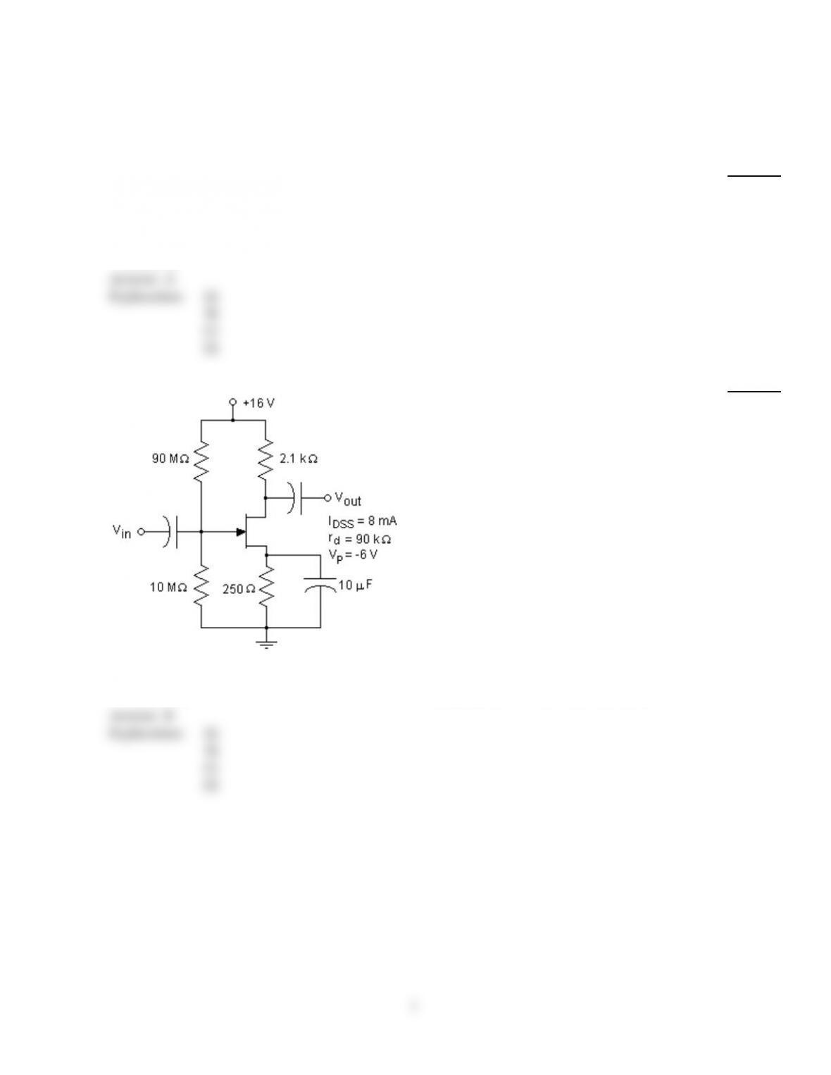
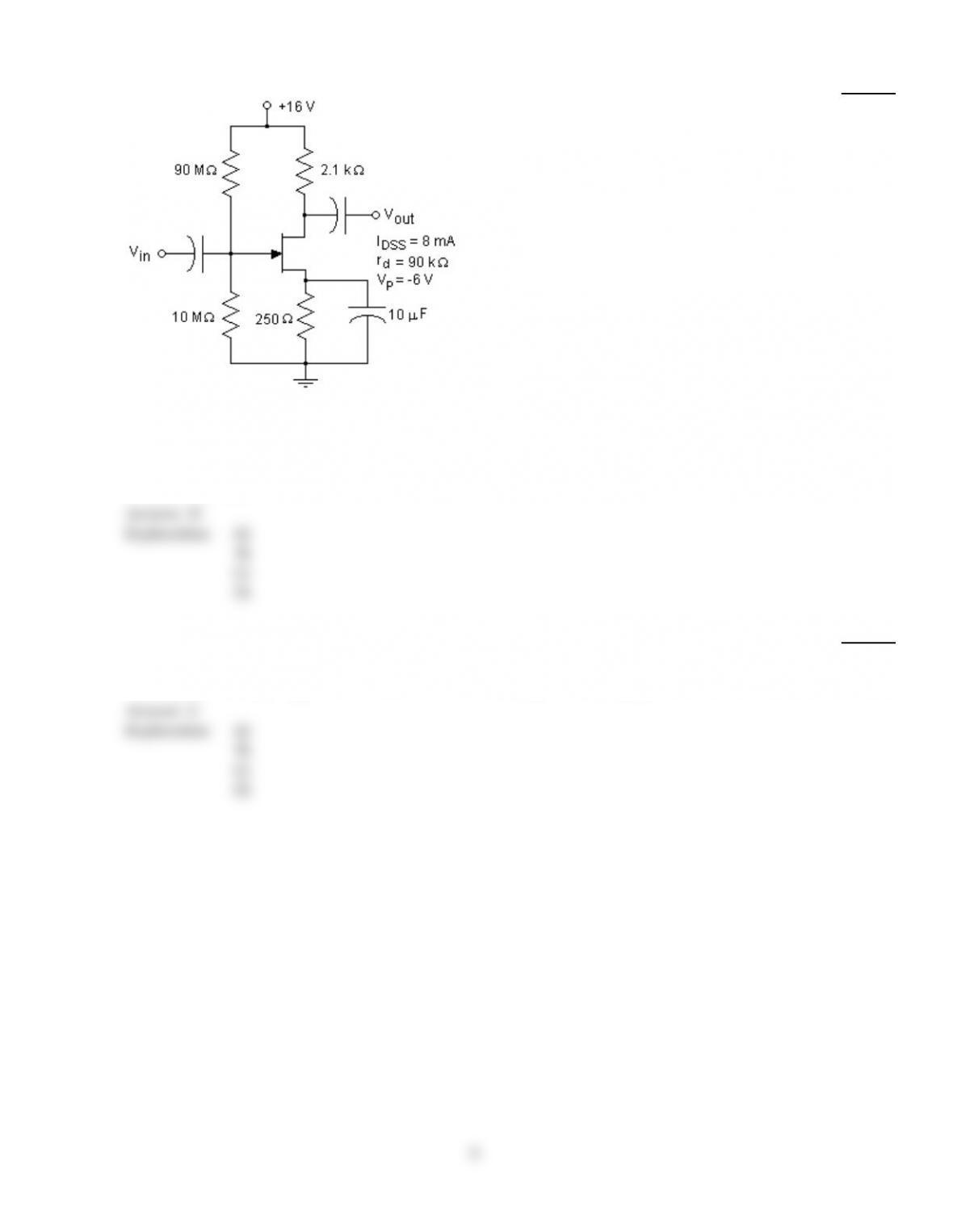
Calculate the output impedance for this FET amplifier.
2)
A)
Zo=RD= 2.1 k
B)
Zo=RDrd= 2052
C)
Zo=rd= 90 k
D)
Zo depends on the drain current ID.
Answer:
B
Explanation:
A)
B)
C)
D)
1
3)
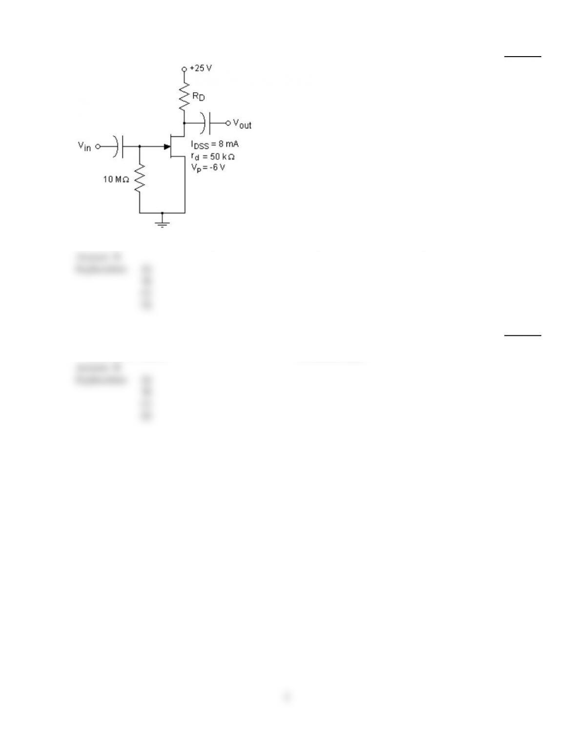
Design this amplifier for a voltage gain of 8, and indicate the required value of resistor RD.
3)
A)
RD= 3.0 k
B)
RD= 3103.44
C)
RD= 9.0 k
D)
RD= 10.0 k
Answer:
B
Explanation:
A)
B)
C)
D)
4)
The FET version of the BJT’s common–emitter configuration is the ________ circuit.
4)
A)
common–drain
B)
common–source
C)
common–current
D)
common–gate
Answer:
B
Explanation:
A)
B)
C)
D)
2
5)
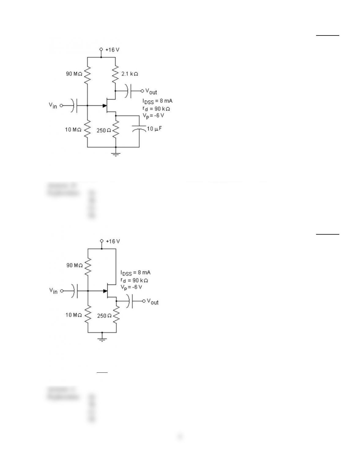
Calculate the voltage gain for this FET amplifier. Assume that the transconductance (gm) for this
circuit is 1.85 mS.
5)
A)
Av depends on the drain current, ID.
B)
Av= –gmrd= –166.5
C)
Av= –gmRD= –3.885
D)
Av= –gm(RD
rd) = –3.7962
Answer:
D
Explanation:
A)
B)
C)
D)
6)
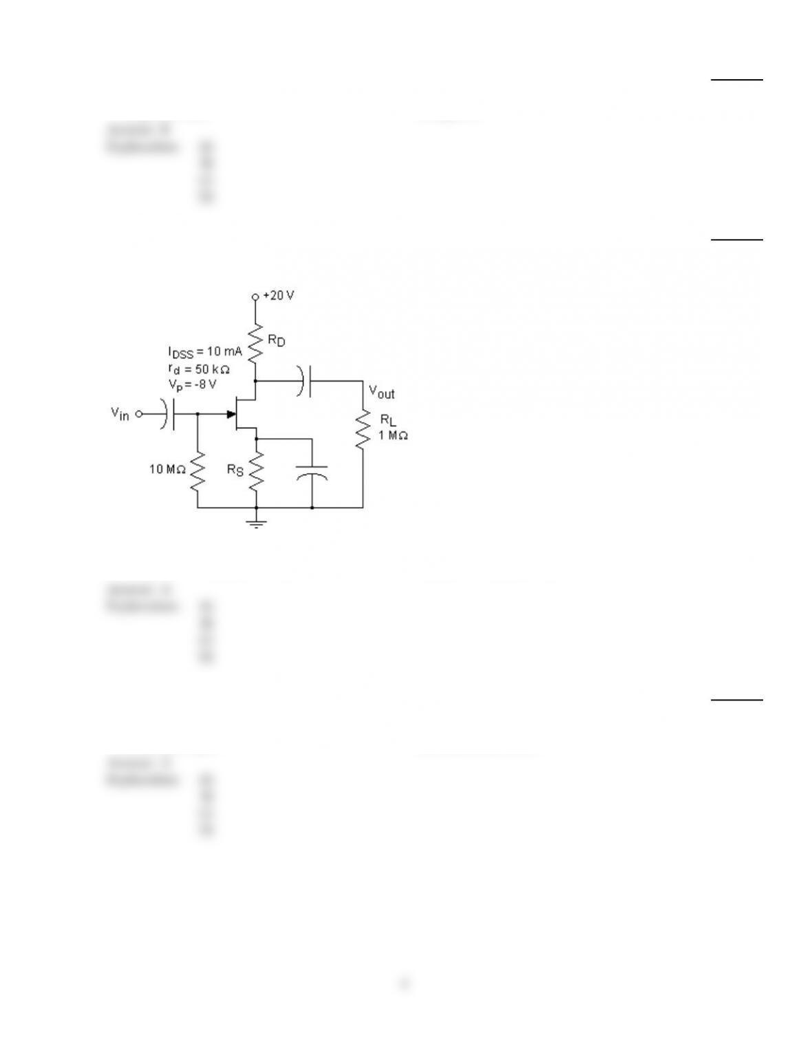
Calculate the output impedance for this FET amplifier. Assume that gm= 1.85 mS.
6)
A)
Zo=RS= 250
B)
Zo depends on the value of ID.
C)
Zo=RSrd1
gm= 170.6
D)
Zo=rd= 90 k
Answer:
C
Explanation:
A)
B)
C)
D)
3
7)
The operating value of gm is always ________ the value of gmo for a given JFET.
7)
A)
less than
B)
less than or equal to
C)
greater than
D)
equal to
Answer:
B
Explanation:
A)
B)
C)
D)
8)
Design this circuit for a voltage gain of 10. You have to calculate the value of resistors RD and RS. It
is desired that the transistor operate with a relatively high value of gm. For this device, a high
value of gm is defined as VGS= 0.2 VP.
8)
A)
RD= 5.555 k, RS= 250
B)
RD= 9.0 k, RS= 1.0 k
C)
RD= 5.555 k, RS= 1.0 k
D)
RD= 9.0 k, RS= 250
Answer:
A
Explanation:
A)
B)
C)
D)
9)
The ________ FET amplifier has high input impedance, low output impedance, and low voltage
gain.
9)
A)
common–drain
B)
common–source
C)
common–gate
D)
None of the above
Answer:
A
Explanation:
A)
B)
C)
D)
4
10)
The ________ FET amplifier has low input impedance, high output impedance, and high voltage
gain.
10)
A)
common–drain
B)
common–source
C)
common–gate
D)
None of the above
Answer:
C
Explanation:
A)
B)
C)
D)
11)
The current gain io
ii of an FET amplifier is ________.
11)
A)
generally assumed to be zero
B)
depends upon the value of gm for the device
C)
less than or equal to 1
D)
undefined
Answer:
D
Explanation:
A)
B)
C)
D)
12)
A given JFET has values of gmo = 1200 µS and VGSOFF = –4 V. What is the value of gm for the
device at VGS= –2 V?
12)
A)
600 µ.S
B)
300 µ.S
C)
1200 µ.S
D)
Cannot be determined from the information given
Answer:
A
Explanation:
A)
B)
C)
D)
5
13)
Calculate the input impedance for this FET amplifier.
13)
A)
Zi=R1= 90 M
B)
Zi= would depend on the drain current ID.
C)
Zi=R2= 10 M
D)
Zi=R1R2= 9 M
Answer:
D
Explanation:
A)
B)
C)
D)
14)
The maximum value of gm occurs where ________ and the minimum value occurs when ________.
14)
A)
ID=IDSS, VGS=Vp
B)
VGS=Vp , VGS= 0 V
C)
VGS= 0 V, VGS=Vp
D)
VGS= 0 V, ID=IDSS,
Answer:
C
Explanation:
A)
B)
C)
D)
6
15)
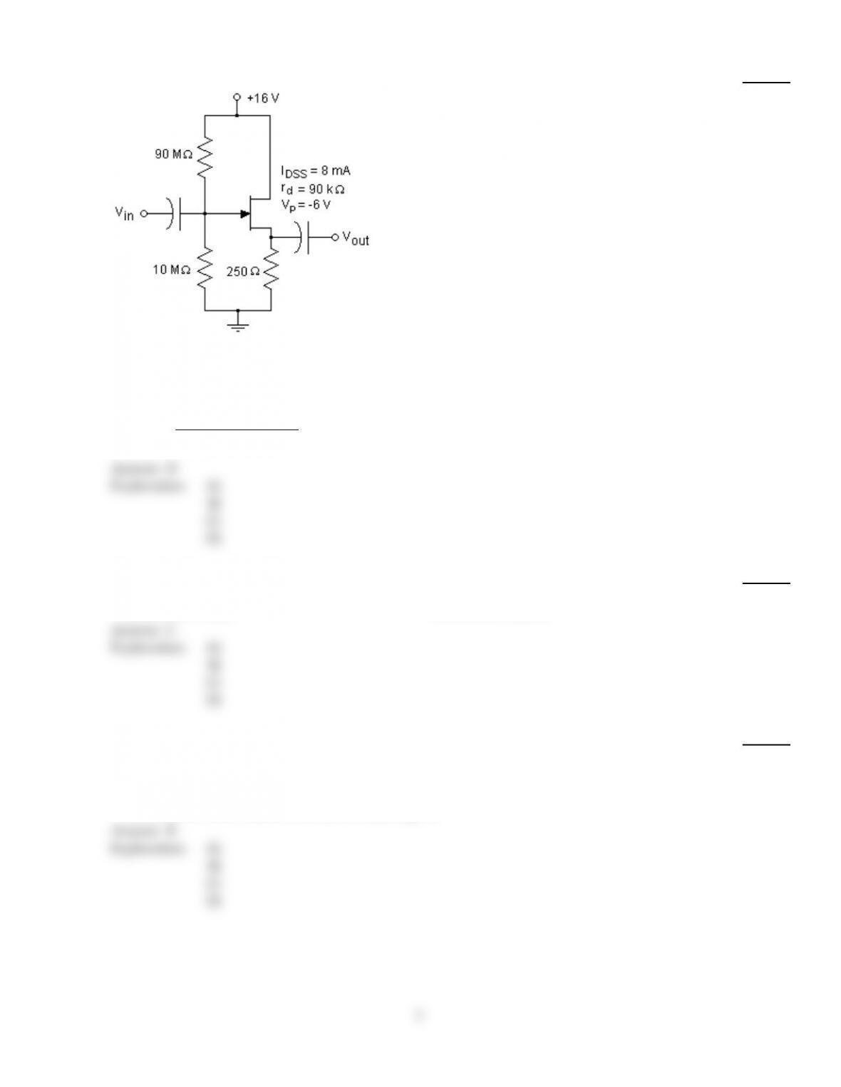
Calculate the voltage gain for this FET amplifier. Assume that gm= 1.85 mS.
15)
A)
Av=gmrd= 166.5
B)
Av=gmRS= 0.462
C)
Av would depend on the drain current, ID.
D)
Av=–gm(rdR1R2)
1 +gm(rdR1R2)= 0.9939
Answer:
D
Explanation:
A)
B)
C)
D)
16)
A source–follower FET configuration is also know as ________ circuit.
16)
A)
current–controlled
B)
common–gate
C)
common–drain
D)
common–source
Answer:
C
Explanation:
A)
B)
C)
D)
17)
A JFET has values of gmo= 1200 µ.S and VGSOFF = –4 V. What is the approximate value of IDSS?
17)
A)
9.6 mA
B)
2.4 mA
C)
4.8 mA
D)
Cannot be determined from the information given
Answer:
B
Explanation:
A)
B)
C)
D)
7
18)
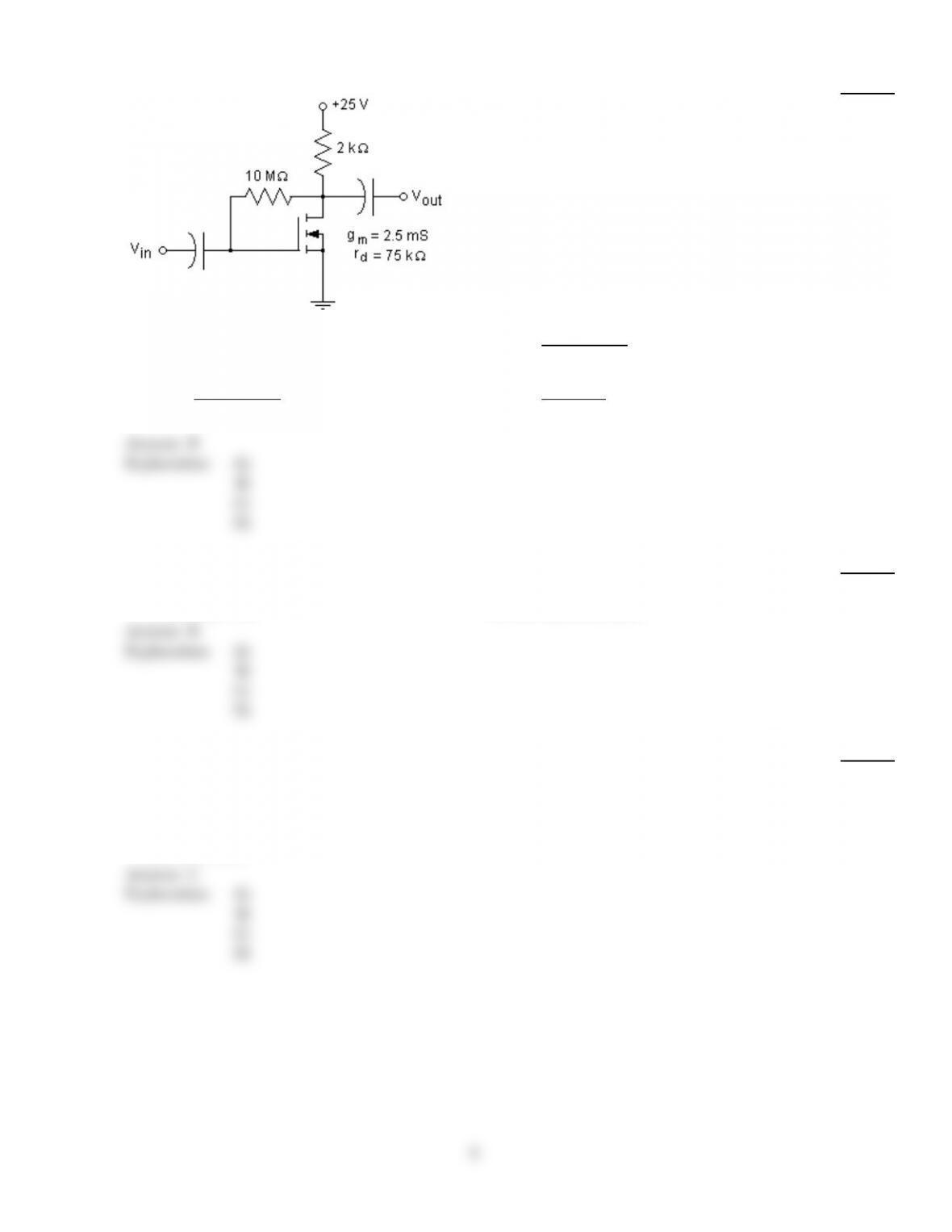
Calculate the input impedance for this E–MOSFET circuit.
18)
A)
Zi=RF= 10.0 M
B)
Zi=RF
1 + (rdRD)= 1.0735 M
C)
Zi=RF
1 + (rdRD)= 5.130 k
D)
Zi=RF
1 +gmrd= 53.05 k
Answer:
B
Explanation:
A)
B)
C)
D)
19)
The unit of measure for FET transconductance ( gm) is ________.
19)
A)
volts per ampere
B)
Siemens
C)
ohms per volt
D)
The term is unitless
Answer:
B
Explanation:
A)
B)
C)
D)
20)
If the resistor bypass capacitor in the source leg is removed, the voltage gain of the small signal FET
amplifier ________.
20)
A)
may increase in some cases and decrease in other cases
B)
will stay the same
C)
will decrease
D)
will increase
Answer:
C
Explanation:
A)
B)
C)
D)
8
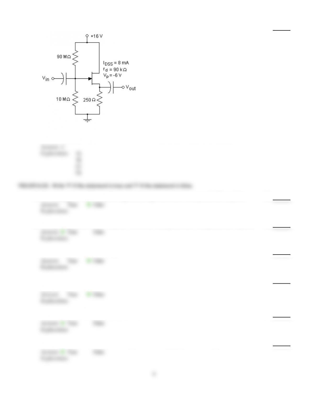
21)
Calculate the input impedance for this amplifier. Assume that gm= 1.85 mS.
21)
A)
Zi=R2= = 10 M
B)
Zi=R1= 90 M
C)
Zi=R1R2= 9 M
D)
Zi depends on the value of ID.
Answer:
C
Explanation:
A)
B)
C)
D)
TRUE/FALSE. Write ‘T’ if the statement is true and ‘F’ if the statement is false.
22)
The voltage gain of a FET amplifier is generally larger than that of a comparable BJT amplifier.
22)
Answer:
True
False
Explanation:
23)
The input impedance of a FET amplifier tends to be much greater than a comparable BJT amplifier.
23)
Answer:
True
False
Explanation:
24)
The value of gm increases as ID approaches 0 mA.
24)
Answer:
True
False
Explanation:
25)
The output impedance of a BJT amplifier tends to be much less than that of a comparable FET
amplifier.
25)
Answer:
True
False
Explanation:
26)
The value of gm increases as VGS approaches 0 V.
26)
Answer:
True
False
Explanation:
27)
The transconductance factor for a FET amplifier is inversely proportional to VGS.
27)
Answer:
True
False
Explanation:
9
28)
A FET amplifier is considered a voltage–controlled device, whereas a BJT is a current–controlled
device.
28)
Answer:
True
False
Explanation:
29)
The transconductance factor for a FET amplifier is inversely proportional to ID.
29)
Answer:
True
False
Explanation:
30)
The values of fs , gfs, and gm are the same.
30)
Answer:
True
False
Explanation:
31)
The input current for a FET amplifier is generally assumed to be zero.
31)
Answer:
True
False
Explanation:
10
Answer Key
Testname: C8
1)
A
2)
B
3)
B
4)
B
5)
D
6)
C
7)
B
8)
A
9)
A
10)
C
11)
D
12)
A
13)
D
14)
C
15)
D
16)
C
17)
B
18)
B
19)
B
20)
C
21)
C
22)
FALSE
23)
TRUE
24)
FALSE
25)
FALSE
26)
TRUE
27)
TRUE
28)
TRUE
29)
FALSE
30)
TRUE
31)
TRUE