
Exam
Name___________________________________
MULTIPLE CHOICE. Choose the one alternative that best completes the statement or answers the question.
1)
When a BJT has its base–emitter junction forward biased and its collector–base junction reverse
biased, it is biased in the ________.
1)
A)
passive region
B)
saturation region
C)
active region
D)
cutoff region
Answer:
C
Explanation:
A)
B)
C)
D)
2)
When a BJT transistor is used in a switching circuit, it operates in the ________.
2)
A)
saturation and cutoff regions
B)
saturation and active regions
C)
active region only
D)
active and cutoff regions
Answer:
A
Explanation:
A)
B)
C)
D)
3)
A Darlington amplifier has values of 1 = 150 and 2 = 50. The net beta for this configuration is
________
3)
A)
7500
B)
100
C)
200
D)
15,000
Answer:
A
Explanation:
A)
B)
C)
D)
4)
When voltage–divider bias is used, it is considered appropriate to use the approximate analysis to
determine the bias condition when the resistance R2 is ________ (l+)RE.
4)
A)
very much less than
B)
less than
C)
very much greater than
D)
greater than
Answer:
C
Explanation:
A)
B)
C)
D)
5)
A(n) ________ configuration ties the collector of one transistor to the emitter of a second transistor.
5)
A)
cascade
B)
direct coupled
C)
cascode
D)
Miller
Answer:
C
Explanation:
A)
B)
C)
D)
1
6)
When a BJT is biased in the cut–off region, its base–emitter junction is ________–biased and its
collector–base junction is ________–biased.
6)
A)
reverse; forward
B)
reverse; reverse
C)
forward; reverse
D)
forward; forward
Answer:
B
Explanation:
A)
B)
C)
D)
7)
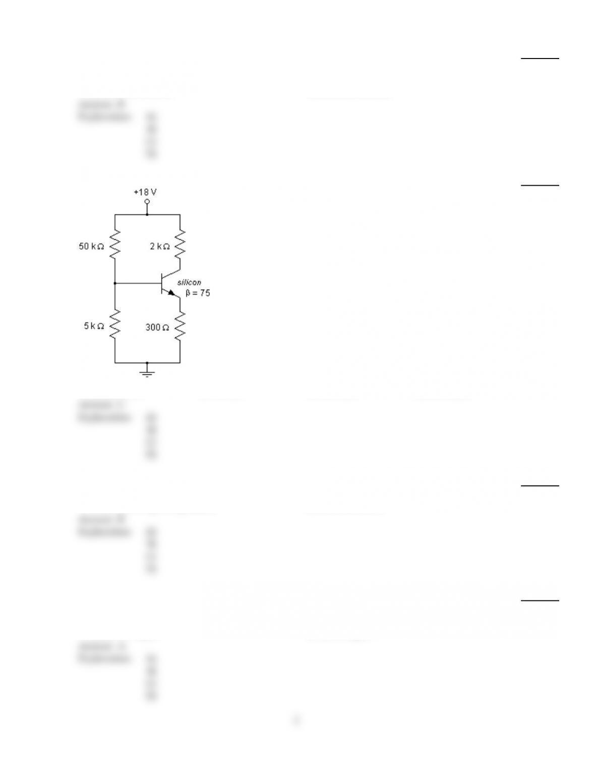
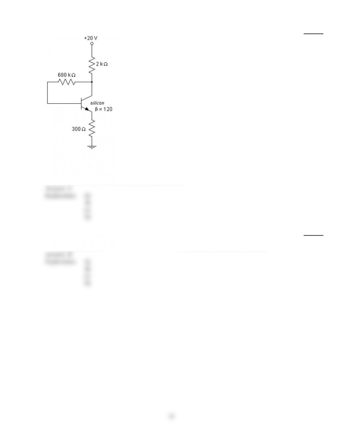
Calculate the base current for this voltage–divider bias circuit.
7)
A)
596.55 µA
B)
76.8 µA
C)
34.37 µA
D)
233.78 µA
Answer:
C
Explanation:
A)
B)
C)
D)
8)
The main benefit of a direct–coupled amplifier is ________.
8)
A)
improved high–frequency response
B)
improved low–frequency response
C)
increased input impedance
D)
all of the above
Answer:
B
Explanation:
A)
B)
C)
D)
9)
When a BJT has its base–emitter junction forward biased and its collector–base junction also
forward biased, it is in the ________.
9)
A)
saturation region
B)
passive region
C)
cut–off region
D)
active region
Answer:
A
Explanation:
A)
B)
C)
D)
2
10)
The change in and VCE that can occur when the temperature changes is known as ________.
10)
A)
midpoint movement
B)
Q–point movement
C)
midpoint bias
D)
output movement
Answer:
B
Explanation:
A)
B)
C)
D)
11)
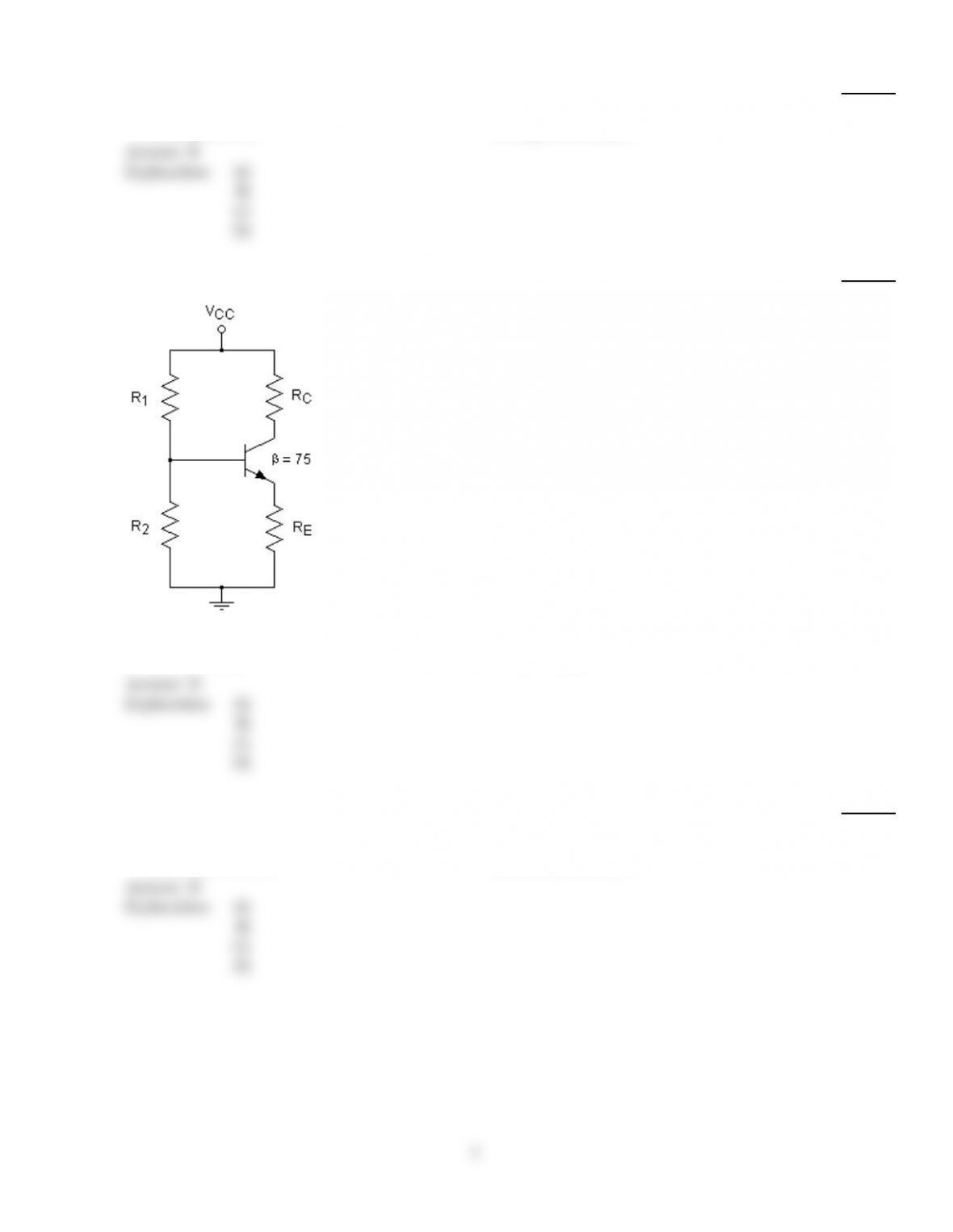
When designing a current–gain–stabilized voltage–divider bias circuit such as this one, the rule of
thumb used for the emitter voltage is ________.
11)
A)
VC=VCC / 10
B)
VB=VCC / 10
C)
VCE =VCC / 10
D)
VE=VCC / 10
Answer:
D
Explanation:
A)
B)
C)
D)
12)
When a BJT is biased in the saturation region, its base–emitter junction is ________–biased and its
collector–base junction is ________–biased.
12)
A)
reverse; reverse
B)
reverse; forward
C)
forward; reverse
D)
forward; forward
Answer:
D
Explanation:
A)
B)
C)
D)
3

13)
When a BJT is biased in the cutoff region the collector–to–emitter voltage is typically equal to
________.
13)
A)
the collector current times the collector resistor
B)
the collector supply voltage
C)
0.03 V
D)
the emitter voltage
Answer:
B
Explanation:
A)
B)
C)
D)
14)
When a transistor is in saturation, the total collector current is limited by ________.
14)
A)
collector–to–emitter and collector supply voltage
B)
the transistor
C)
collector supply, collector–to–emitter voltage, and the total collector circuit resistance
D)
collector supply voltage and the total resistance in the collector and emitter circuits
Answer:
D
Explanation:
A)
B)
C)
D)
15)
The collector–feedback bias configuration’s input resistance is related to the ________.
15)
A)
emitter resistor
B)
collector resistor
C)
base feedback resistor
D)
device beta
Answer:
D
Explanation:
A)
B)
C)
D)
4
16)
Calculate the collector–emitter voltage for this emitter–stabilized circuit.
16)
A)
10.68 V
B)
4.28 V
C)
14.24 V
D)
0.1335 V
Answer:
B
Explanation:
A)
B)
C)
D)
17)
When a BJT is in cutoff, the collector–to–emitter voltage is typically equal to ________.
17)
A)
collector supply voltage
B)
emitter voltage
C)
collector current times collector resistor
D)
0.3 Volts
Answer:
A
Explanation:
A)
B)
C)
D)
18)
Calculate the base current for this circuit.
18)
A)
0.056 mA
B)
0.96 mA
C)
0.904 mA
D)
6.0 mA
Answer:
C
Explanation:
A)
B)
C)
D)
5

19)
Collector–feedback bias ________.
19)
A)
provides a feedback path from collector to base
B)
is not totally independent of beta
C)
provides an improved level of stability over fixed–bias
D)
All of the above
Answer:
D
Explanation:
A)
B)
C)
D)
20)
The term quiescent means ________.
20)
A)
active
B)
at rest
C)
midpoint–biased
D)
inactive
Answer:
D
Explanation:
A)
B)
C)
D)
21)
The most common means of producing multiple BJT networks is ________.
21)
A)
open–stage coupling
B)
transformer coupling
C)
direct coupling
D)
R–C coupling
Answer:
D
Explanation:
A)
B)
C)
D)
22)
The base current for the circuit below is ________.
22)
A)
6 mA
B)
0.94 mA
C)
12 mA
D)
1.37 mA
Answer:
B
Explanation:
A)
B)
C)
D)
23)
Assume that you notice in a complex network that many of the transistors do not have their
collector leads connected. This means that the transitors are most likely ________.
23)
A)
being used as diodes
B)
being used as variable resistors
C)
redundant
D)
being used as buffers
Answer:
A
Explanation:
A)
B)
C)
D)
6
24)
The Common–base configuration is unique in the it ________.
24)
A)
has its output taken from the emitter terminal
B)
has an inverted output
C)
has very high input impedance
D)
has its output taken from the base terminal
Answer:
A
Explanation:
A)
B)
C)
D)
25)
The emitter–follower configuration has ________.
25)
A)
the emitter connected to dc ground potential
B)
an output voltage slightly greater than the input voltage
C)
a 180° phase shift
D)
None of the above
Answer:
D
Explanation:
A)
B)
C)
D)
26)
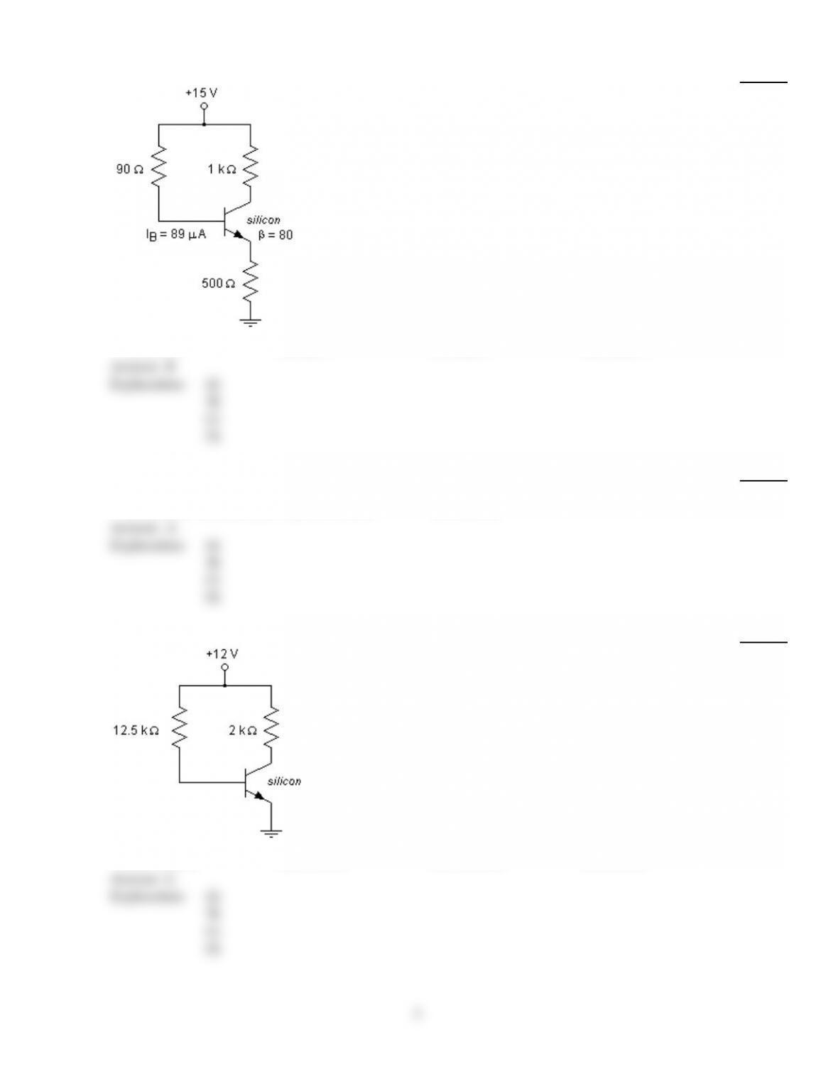
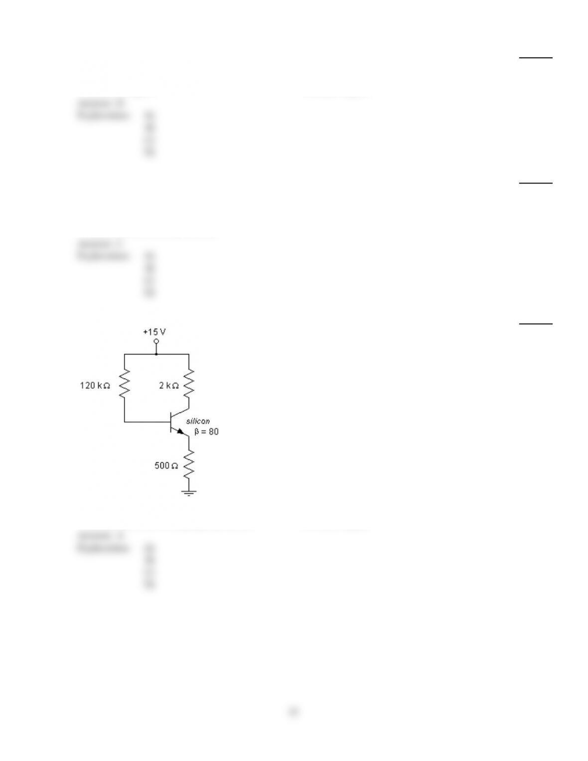
Calculate the base current for this emitter–stabilized bias circuit.
26)
A)
89.1 µA
B)
89.0 mA
C)
0.119 mA
D)
None of the above
Answer:
A
Explanation:
A)
B)
C)
D)
7

27)
To design a transistor circuit for maximum stability, one must consider ________.
27)
A)
the transistor’s beta stability factor
B)
the collector leakage current stability factor
C)
the base–emitter junction voltage stability factor
D)
All of the above
Answer:
D
Explanation:
A)
B)
C)
D)
28)
The difference between the resulting equations for a network in which an npn transistor has been
replaced by a pnp transistor is ________.
28)
A)
the sign associated with the particular quantities
B)
the values of the resistors
C)
the value of
D)
All of the above
Answer:
A
Explanation:
A)
B)
C)
D)
29)
In the design of an emitter–bias stabilized circuit engineering, judgment must be used because the
________.
29)
A)
emitter resistor is usually unknown
B)
relative voltage levels have not been defined
C)
collector resistor is usually unknown
D)
All of the above
Answer:
D
Explanation:
A)
B)
C)
D)
30)
When a BJT is biased in the active region, its base–emitter junction is ________–biased and its
collector–base junction is ________–biased.
30)
A)
forward; reverse
B)
reverse; forward
C)
reverse; reverse
D)
forward; forward
Answer:
A
Explanation:
A)
B)
C)
D)
8

31)
There are transistors that are called switching transistors because ________.
31)
A)
of the power they can transfer from input to output
B)
of the voltage they can transfer from input to output
C)
of the speed at which they can be changed from on to off
D)
they have a built in switch
Answer:
C
Explanation:
A)
B)
C)
D)
32)
A(n) ________ is added to the fixed–bias configuration to improve bias stability.
32)
A)
collector resistor
B)
base voltage
C)
emitter resistor
D)
All of the above
Answer:
C
Explanation:
A)
B)
C)
D)
33)
Transistor circuits that are quite stable and relatively insensitive to temperature variations have
________.
33)
A)
relative high supply voltages
B)
large betas
C)
small betas
D)
low supply voltages
Answer:
B
Explanation:
A)
B)
C)
D)
34)
When designing for best bias stability the ________ configuration should be chosen.
34)
A)
emitter–feedback bias
B)
collector–feedback bias
C)
fixed–bias
D)
voltage–divider bias
Answer:
D
Explanation:
A)
B)
C)
D)
35)
Why is design for a specific bias point desirable for most amplifiers?
35)
A)
It allows optimum ac operation of the circuit.
B)
It allows optimum dc operation of the circuit.
C)
To meet manufacturer suggested opening point.
D)
All of the above
Answer:
D
Explanation:
A)
B)
C)
D)
9

36)
The input resistance of a stabilized fixed–bias circuit configuration is ________.
36)
A)
inversely related to
B)
directly related to the collector resistor
C)
directly related to the emitter resistor
D)
inversely related to the emitter resistor
Answer:
C
Explanation:
A)
B)
C)
D)
37)
Two of the factors associated with bias stability are ________.
37)
A)
age and amount of use
B)
the and the junction temperature
C)
voltage and current
D)
None of the above
Answer:
B
Explanation:
A)
B)
C)
D)
38)
When designing a voltage–divider bias circuit, the divider resistors ________.
38)
A)
should carry approximately equal current
B)
determine the base voltage as the drop across base–common resistor
C)
should carry currents that are 10 times the base current
D)
All of the above
Answer:
D
Explanation:
A)
B)
C)
D)
39)
If a zener diode is connected to the base of a transistor, chances are it is a ________ .
39)
A)
beta–stabilized circuit
B)
current mirror
C)
gain–stabilized amplifier
D)
constant–current source
Answer:
D
Explanation:
A)
B)
C)
D)
40)
A collector–feedback bias circuit is found to be in saturation. Which of the following could cause
this condition?
40)
A)
A solder bridge across the base resistor.
B)
The collector resistor is open.
C)
The transistor is shorted base–to–emitter.
D)
The base resistor is open.
Answer:
A
Explanation:
A)
B)
C)
D)
10
41)
Calculate the base current for this circuit.
41)
A)
28.3 µA
B)
28.4 µA
C)
20.2 µA
D)
Need more information to calculate the base current
Answer:
C
Explanation:
A)
B)
C)
D)
42)
Voltage–divider bias stability is ________.
42)
A)
dependent on alpha
B)
independent of beta
C)
dependent of beta
D)
dependent on the collector resistor
Answer:
B
Explanation:
A)
B)
C)
D)
11
43)
The maximum collector current for this circuit is ________.
43)
A)
1.0 mA
B)
1.13 mA
C)
12 mA
D)
6 mA
Answer:
D
Explanation:
A)
B)
C)
D)
44)
The first transistor in a feedback pair ________.
44)
A)
is an npn
B)
is inverted
C)
always has the higher beta value
D)
is a pnp
Answer:
D
Explanation:
A)
B)
C)
D)
45)
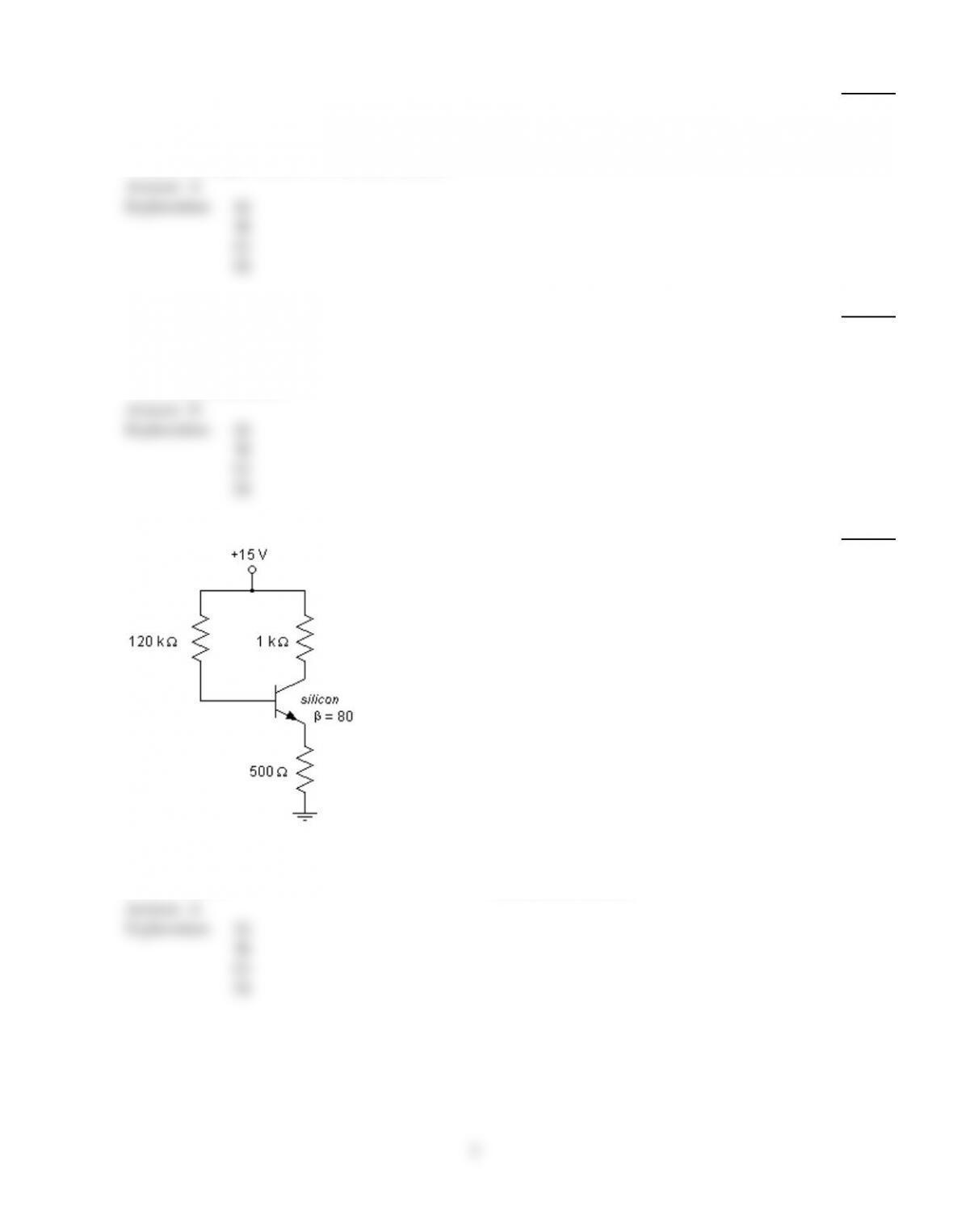
Calculate the maximum collector current for this circuit.
45)
A)
0.056 mA
B)
0.96 mA
C)
0.904 mA
D)
6.0 mA
Answer:
D
Explanation:
A)
B)
C)
D)
12
46)
When a BJT has its base–emitter junction reverse biased and its collector–base junction reverse
biased, it is in the ________.
46)
A)
saturation region
B)
passive region
C)
active region
D)
cutoff region
Answer:
D
Explanation:
A)
B)
C)
D)
47)
Variation in hfe is influenced by ________.
47)
A)
temperature and base current
B)
bias type and device size
C)
junction temperature and collector current
D)
device size and base current
Answer:
C
Explanation:
A)
B)
C)
D)
48)
This emitter–stabilized bias circuit is operating in the ________.
48)
A)
saturation region
B)
active region
C)
The transistor is not properly biased.
D)
cutoff region
Answer:
A
Explanation:
A)
B)
C)
D)
13

49)
When a BJT has its base–emitter junction reverse biased and its base–collector junction forward
biased, it is biased in the ________.
49)
A)
passive region
B)
saturation region
C)
active region
D)
cutoff region
Answer:
D
Explanation:
A)
B)
C)
D)
14

Answer Key
Testname: C4
1)
C
2)
A
3)
A
4)
C
5)
C
6)
B
7)
C
8)
B
9)
A
10)
B
11)
D
12)
D
13)
B
14)
D
15)
D
16)
B
17)
A
18)
C
19)
D
20)
D
21)
D
22)
B
23)
A
24)
A
25)
D
26)
A
27)
D
28)
A
29)
D
30)
A
31)
C
32)
C
33)
B
34)
D
35)
D
36)
C
37)
B
38)
D
39)
D
40)
A
41)
C
42)
B
43)
D
44)
D
45)
D
46)
D
47)
C
48)
A
49)
D