Exam
Name___________________________________
MULTIPLE CHOICE. Choose the one alternative that best completes the statement or answers the question.
1)
What is the maximum output voltage for this clamping circuit?
1)
A)
– 21 Volts
B)
– 11 Volts
C)
+ 21 Volts
D)
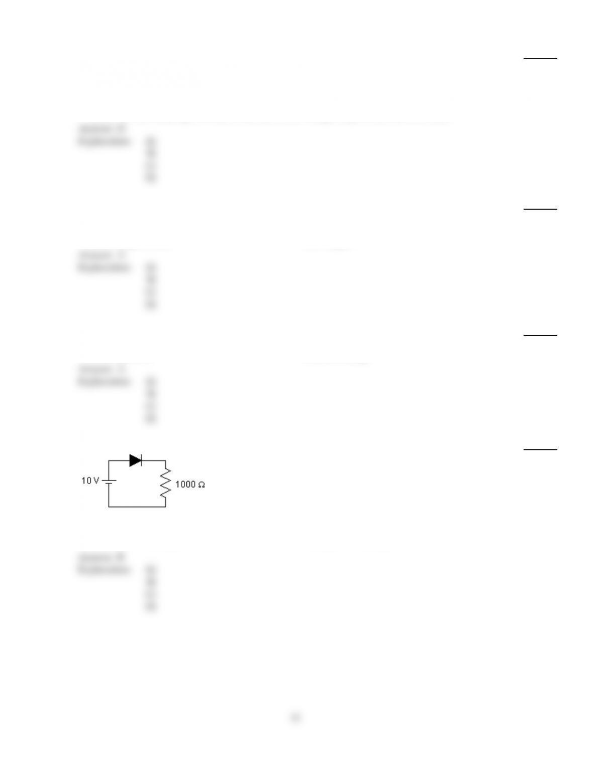
+ 11 Volts
Answer:
C
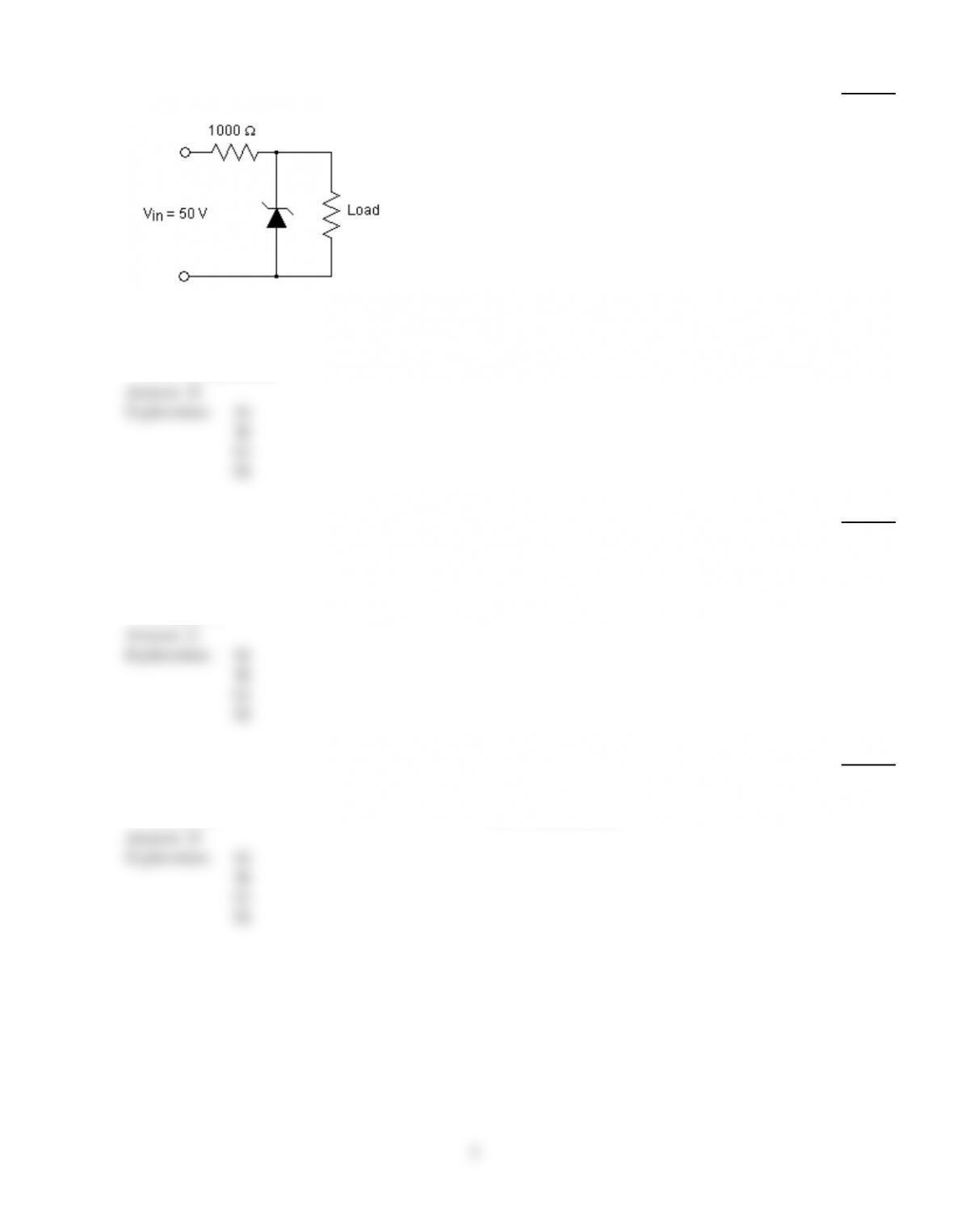
Explanation:
A)
B)
C)
D)
2)
Generally a germanium diode is in the ________ state when the current established by the applied
voltage source is in the direction of the diode symbol’s arrow and VD is greater than or equal to 0.3
V.
2)
A)
saturated
B)
reverse–biased
C)
off
D)
on
Answer:
D
Explanation:
A)
B)
C)
D)
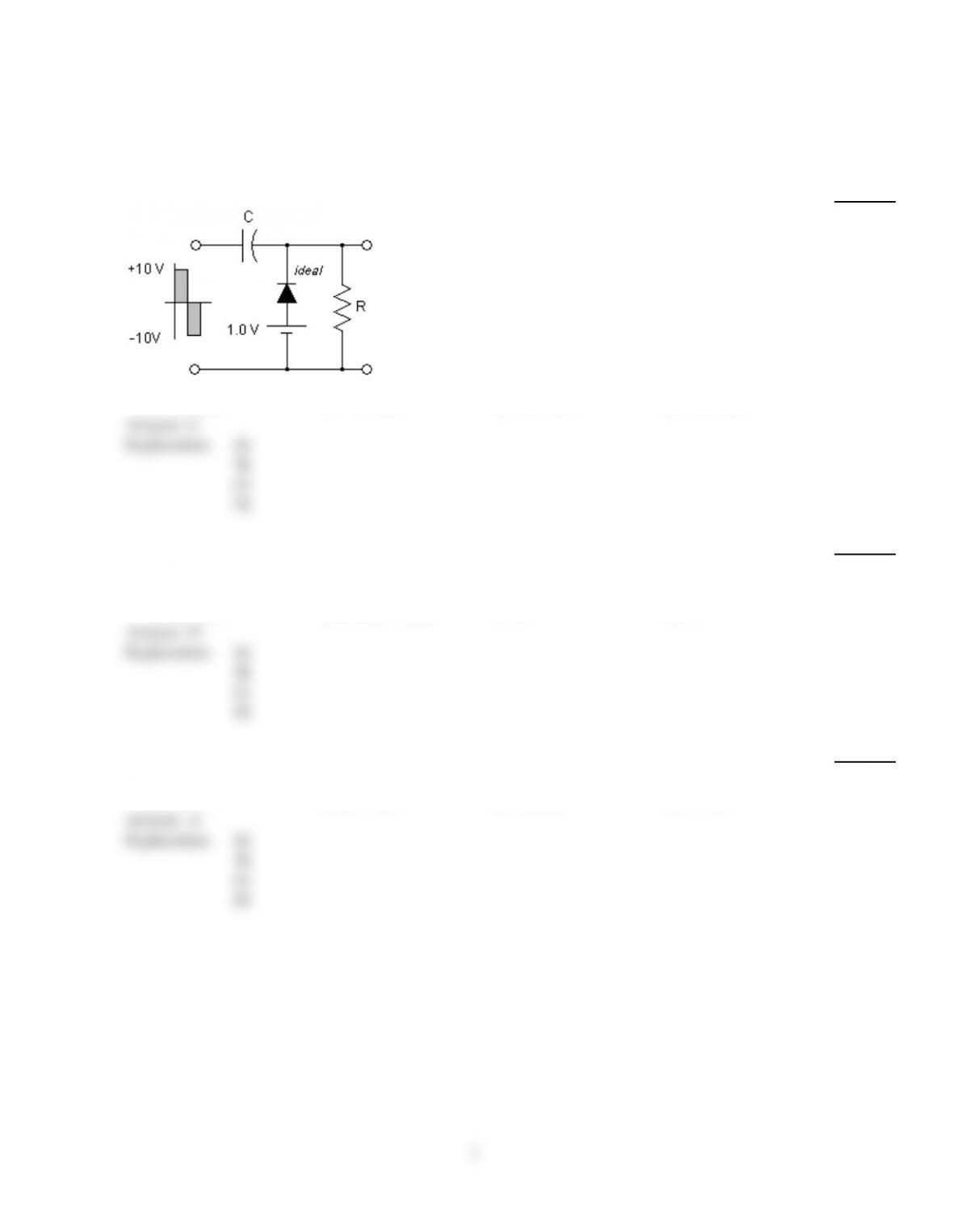
3)
A full–wave center–tapped rectifier has a secondary maximum voltage of 20 Vm and a 4.7 k load
resistance. What is the dc load current for the circuit?
3)
A)
1.26 mA
B)
629.8 mA
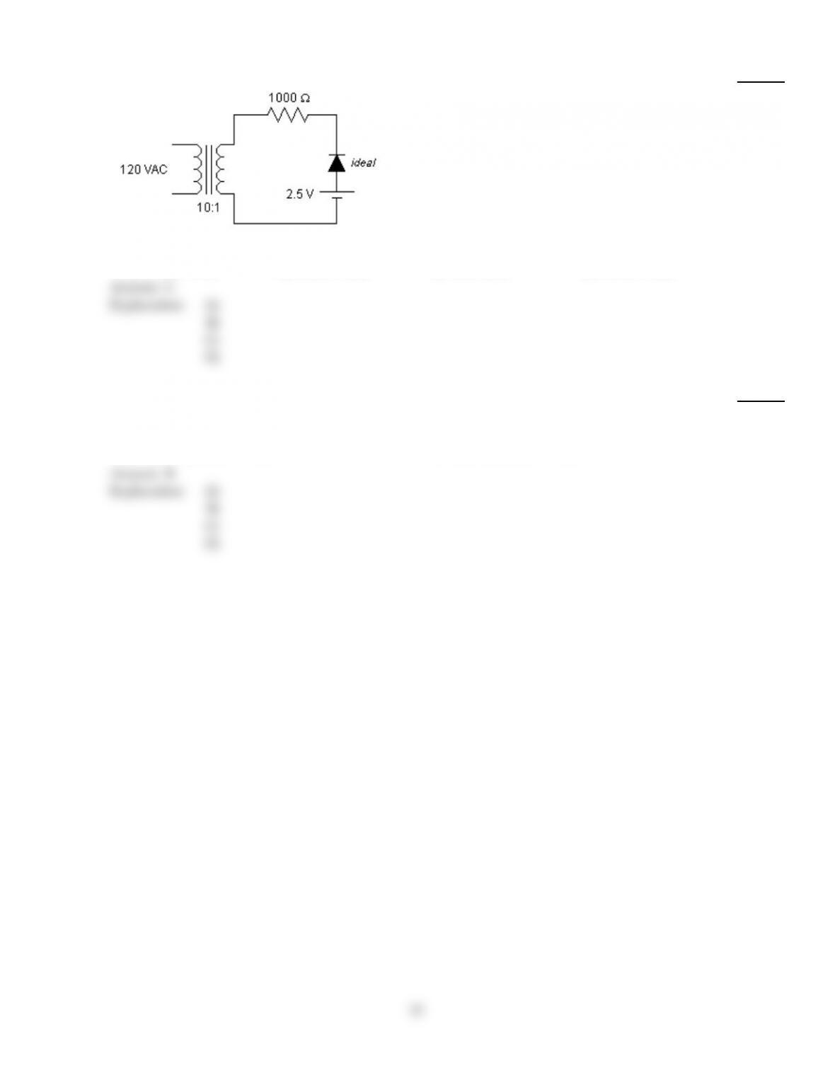
C)
2.61 mA
D)
1.4 mA
Answer:
A
Explanation:
A)
B)
C)
D)
1
4)
What is the minimum output voltage for this clipping circuit when the diode is not conducting?
4)
A)
+ 16.97 V
B)
– 17.97 V
C)
– 16.97 V
D)
0 V
Answer:
D
Explanation:
A)
B)
C)
D)
5)
The two general categories of clippers are ________.
5)
A)
series and parallel
B)
regenerator and eliminator
C)
half–wave and full–wave
D)
dc restorer and dc eliminator
Answer:
A
Explanation:
A)
B)
C)
D)
6)
When analyzing a diode circuit with both a dc and ac source ________.
6)
A)
use superposition
B)
first determine the bulk resistance of the diode
C)
Thevenize the circuit
D)
only the dc source is considered
Answer:
A
Explanation:
A)
B)
C)
D)
7)
When in its “on” state, the voltage across an ideal Zener diode, VZ ________.
7)
A)
gets smaller with an increase in applied voltage
B)
increases sharply with a decrease in applied voltage
C)
gets larger with an increase in applied voltage
D)
None of these
Answer:
D
Explanation:
A)
B)
C)
D)
2
8)
A positive full–wave center–tapped rectifier has a secondary voltage of 20 Vm. The peak load
voltage for the circuit is ________ if the diode drop is included.
8)
A)
20 Vp
B)
10 Vp
C)
19.3 Vp
D)
9.3 Vp
Answer:
D
Explanation:
A)
B)
C)
D)
9)
The circuit shown here is a ________.
9)
A)
shunt clamper
B)
shunt clipper
C)
series clamper
D)
series clipper
Answer:
B
Explanation:
A)
B)
C)
D)
10)
What is the value of the voltage dropped across forward–biased silicon diodes that are connected
in parallel with each other?
10)
A)
1.4 V
B)
11.3 V
C)
0.7 V
D)
0.3 5 V
Answer:
C
Explanation:
A)
B)
C)
D)
11)
Which of the following circuits is used to eliminate a portion of a signal?
11)
A)
Voltage divider
B)
Voltage multiplier
C)
Damper
D)
Clipper
Answer:
D
Explanation:
A)
B)
C)
D)
12)
Generally a silicon diode is in the ________ state if the current established by the applied voltage
source is in the direction of the diode symbol’s arrow and VD is greater than or equal to 0.7 V.
12)
A)
saturated
B)
reverse–biased
C)
off
D)
on
Answer:
D
Explanation:
A)
B)
C)
D)
3
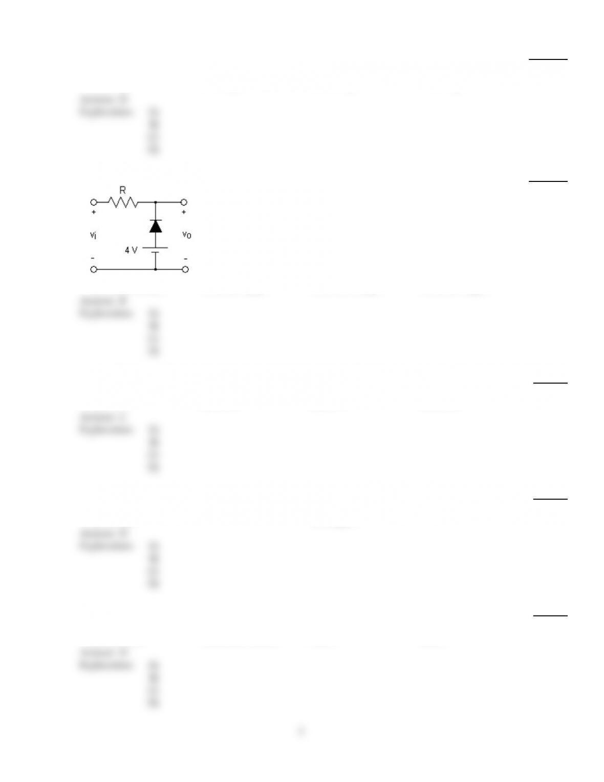
13)
The value of VD in this circuit is ________.
13)
A)
0.7 V
B)
10.6 V
C)
0.3 V
D)
11.3 V
Answer:
C
Explanation:
A)
B)
C)
D)
14)
The practical value of the current IR in this circuit is ________.
14)
A)
0.5 mA
B)
0.5 A
C)
0 A
D)
5 mA
Answer:
C
Explanation:
A)
B)
C)
D)
15)
When a Zener diode circuit is used to stabilize the output voltage given a fixed load resistor and a
variable input voltage, the input voltage must be ________.
15)
A)
large enough to turn on the Zener diode
B)
small enough to turn off the Zener diode
C)
small enough to turn on the Zener diode
D)
large enough to turn off the Zener diode
Answer:
A
Explanation:
A)
B)
C)
D)
4
16)
What are the minimum and maximum values of current flowing in the variable load resistor while
the diode is operating in the Zener region? The zener voltage is 10 V.
16)
A)
8 mA and 35 mA
B)
12.5 mA and 40 mA
C)
Need to know the load resistance to determine the values.
D)
8 mA and 40 mA
Answer:
D
Explanation:
A)
B)
C)
D)
17)
When the diode in a half–wave rectifier points toward the load, the output from the rectifier is
________.
17)
A)
either positive or negative, depending on the polarity of the transformer secondary voltage
B)
full–wave
C)
positive
D)
negative
Answer:
C
Explanation:
A)
B)
C)
D)
18)
The point of intersection between the characteristic curve of the diode and the resistors loadline is
known as the ________.
18)
A)
quiescent point
B)
point of operation
C)
Q–point
D)
All of the above
Answer:
D
Explanation:
A)
B)
C)
D)
5

19)
A typical Zener diode regulator circuit uses a ________.
19)
A)
dropping resistor in series with the load
B)
Zener diode in parallel with the series resistor
C)
Zener diode in series with the load
D)
resistor in parallel with the load
Answer:
A
Explanation:
A)
B)
C)
D)
20)
The Zener diode must be operated such that ________.
20)
A)
the applied voltage is greater than VZ
B)
IZ×VZ=PZ
C)
PZ is less than the specified PZmax
D)
All of these
Answer:
D
Explanation:
A)
B)
C)
D)
21)
Given a series silicon diode circuit with the resistor R = 2 k ohms and an applied voltage of 10 V,
what is IDQ?
21)
A)
0.5 mA
B)
1.0 mA
C)
4.65 mA
D)
10 mA
Answer:
C
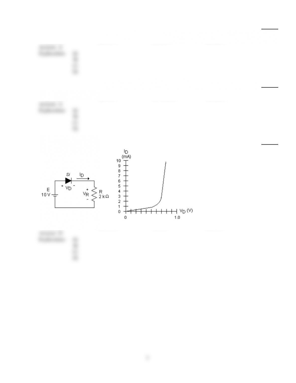
Explanation:
A)
B)
C)
D)
22)
The biased clamper has a dc reference voltage that is ________.
22)
A)
equal to the dc average of the circuits output signal
B)
dependent on the peak–to–peak value of the ac input
C)
approximately equal to zero volts
D)
approximately equal to the dc voltage that is applied to the diode
Answer:
D
Explanation:
A)
B)
C)
D)
23)
Two Zener diodes connected ________ can be used as an ac regulator.
23)
A)
back–to–back
B)
in series with the load
C)
in series with the input voltage
D)
in parallel with each other
Answer:
A
Explanation:
A)
B)
C)
D)
6
24)
A bridge rectifier has values of Vm= 177 V, turns ratio = 5 : 1, and RL= 500 . What is the dc
output voltage?
24)
A)
21.62 V
B)
3.75 V
C)
9.91 V
D)
6.88 V
Answer:
A
Explanation:
A)
B)
C)
D)
25)
A half–wave rectifier with the diode arrow pointing away from the load has a DC output voltage of
________ for an AC input voltage of 20 V maximum.
25)
A)
–6.14 V
B)
19.3 V
C)
–13.65 V
D)
12.49 V
Answer:
A
Explanation:
A)
B)
C)
D)
26)
For this series diode configuration, use the diode characteristic to estimate the value of VR.
26)
A)
0.92 V
B)
92 mV
C)
10 V
D)
9.2 V
Answer:
D
Explanation:
A)
B)
C)
D)
7
27)
The resistor voltage and resistor current in this circuit are ________.
27)
A)
11 V, 2 mA
B)
10 V, 5 mA
C)
11 V, 11 mA
D)
2 V, 11 mA
Answer:
C
Explanation:
A)
B)
C)
D)
28)
The current flows through the load resistor in this circuit during the ________.
28)
A)
negative half cycle of the input waveform
B)
The diode will block all current and there will be no current flowing through the load.
C)
positive half cycle of the input waveform
D)
entire input waveform
Answer:
C
Explanation:
A)
B)
C)
D)
29)
A(n) ________ is commonly used to provide transient protection.
29)
A)
clipper
B)
clamper
C)
eliminator
D)
multiplier
Answer:
A
Explanation:
A)
B)
C)
D)
8
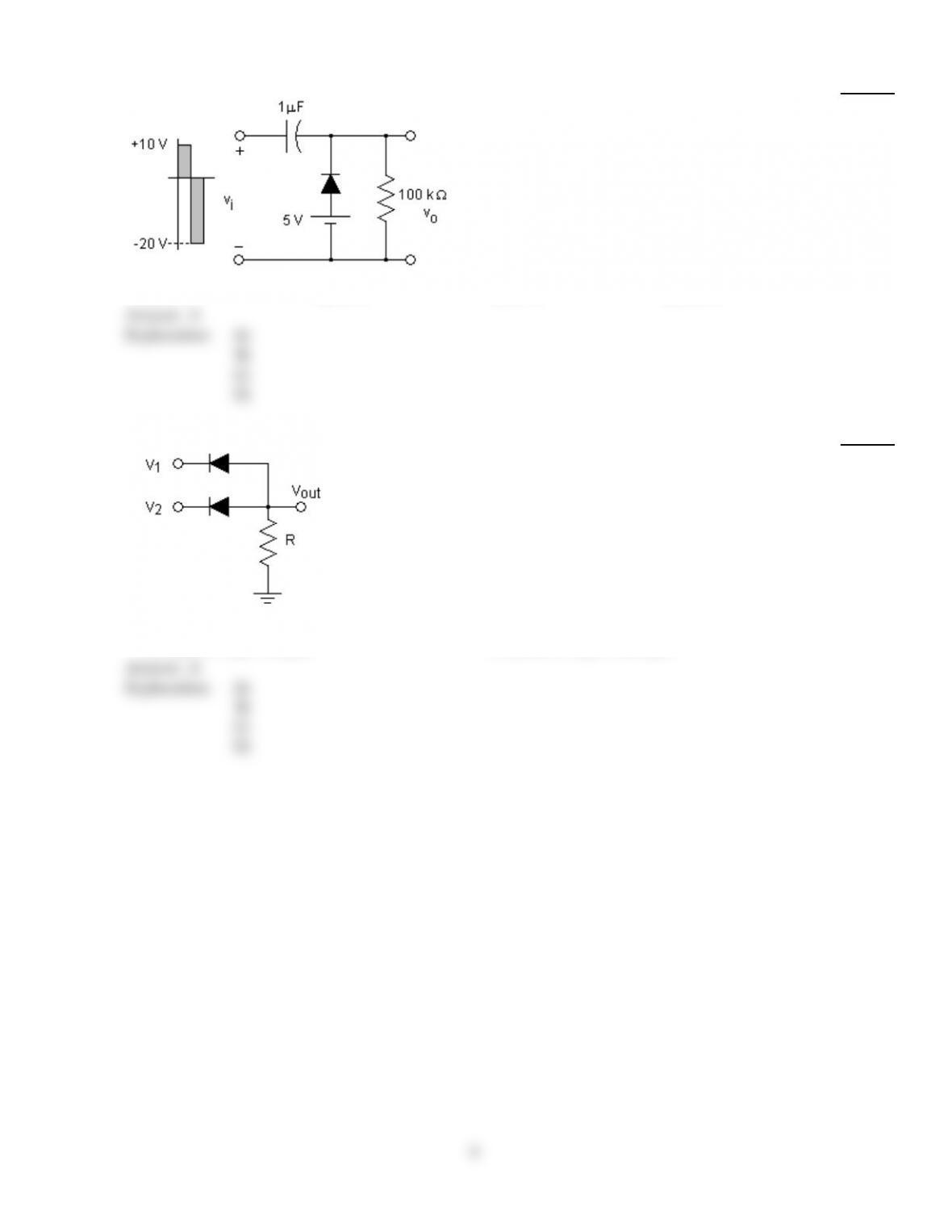
30)
Assuming this circuit uses a silicon diode, the output voltage is clamped to ________.
30)
A)
4.3 V
B)
5.7 V
C)
5.3 V
D)
10.7 V
Answer:
A
Explanation:
A)
B)
C)
D)
31)
Name the logic gate that is formed by this circuit.
31)
A)
positive logic OR gate
B)
negative logic AND gate
C)
negative logic OR gate
D)
positive logic AND gate
Answer:
A
Explanation:
A)
B)
C)
D)
9

32)
For this clipping circuit, what is the minimum output voltage when the diode is conducting?
32)
A)
– 1.0 V
B)
– 17.97 V
C)
– 16.97 V
D)
+ 16.97 V
Answer:
A
Explanation:
A)
B)
C)
D)
33)
A series silicon diode circuit has a 2 k resistor and a 10 V source. Determine VDQ if IDQ is 4.5
mA.
33)
A)
11.5 V
B)
0.7 V
C)
2 V
D)
1 V
Answer:
D
Explanation:
A)
B)
C)
D)
34)
When the output signal to a clamper circuit is clamped to zero, the total swing of the output is
equal to ________.
34)
A)
half the total input voltage swing
B)
half the total voltage drop
C)
the total input voltage swing
D)
the total diode voltage drop
Answer:
C
Explanation:
A)
B)
C)
D)
35)
Why are bridge rectifiers preferred over full–wave center–tapped rectifiers?
35)
A)
They provide higher dc output voltages.
B)
They do not require the use of a center–tapped transformer.
C)
They require a lower PIV rating.
D)
All the above
Answer:
D
Explanation:
A)
B)
C)
D)
10
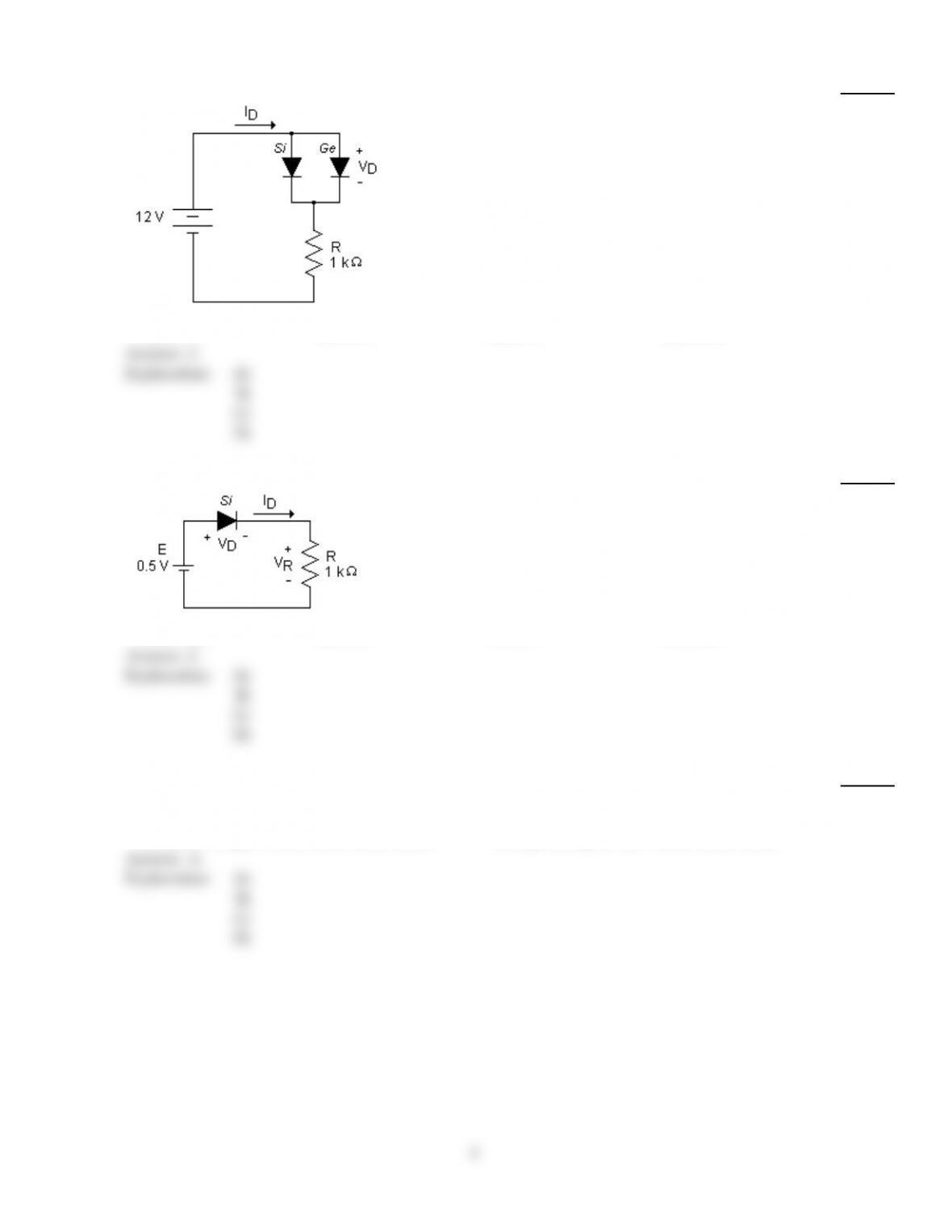
36)
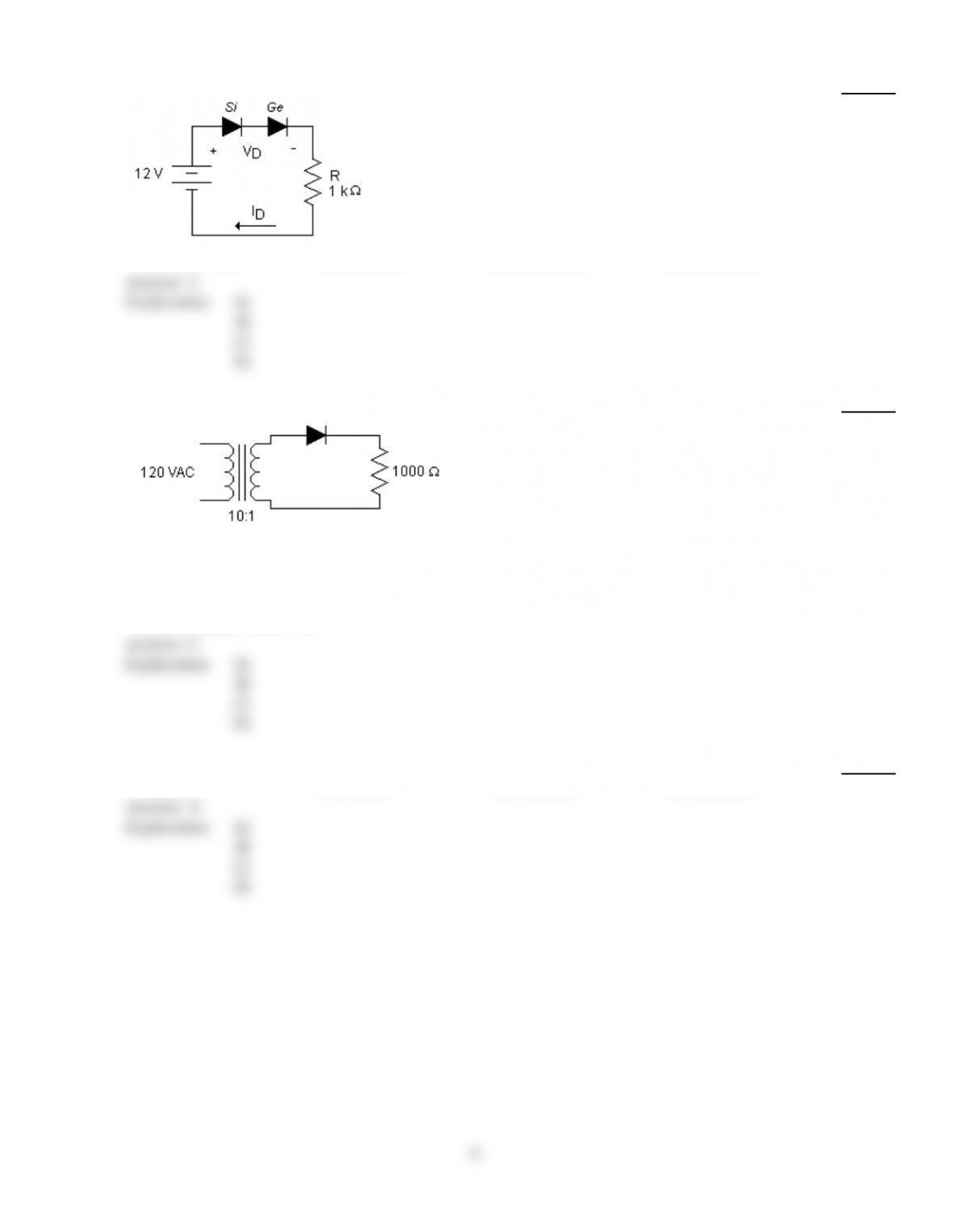
If one silicon diode and one germanium diode are connected in series, the voltage drop across the
combination of the two diodes will be equal to ________.
36)
A)
the forward drop equal to that of the difference of the voltage drops across the two diodes
B)
the forward drop equal to that of the silicon diode
C)
the forward drop equal to that of the germanium diode
D)
the forward drop equal to that of the sum of the voltage drops across the two diodes
Answer:
D
Explanation:
A)
B)
C)
D)
37)
Which of the following circuits is used to change the dc reference of a signal without changing the
shape of the signal?
37)
A)
a clamper
B)
a voltage multiplier
C)
a voltage divider
D)
a clipper
Answer:
A
Explanation:
A)
B)
C)
D)
38)
A Zener diode is designed to operate in the ________ region of its characteristic curve.
38)
A)
reverse breakdown
B)
forward operating
C)
reverse bias
D)
zero voltage
Answer:
A
Explanation:
A)
B)
C)
D)
39)
For this circuit, determine the load–line intersection with the two axis.
39)
A)
VD= 1 V and ID= l mA
B)
VD= 10 V and ID= l0 mA
C)
VD= 10 V and ID= l mA
D)
VD= 1 V and ID= l0 mA
Answer:
B
Explanation:
A)
B)
C)
D)
11
40)
Calculate the peak current that will flow through this circuit, assuming an ideal diode.
40)
A)
16.97 mA during the negative half cycle
B)
16.97 mA during the positive half cycle
C)
12 mA during the negative half cycle
D)
12 mA during the positive half cycle
Answer:
A
Explanation:
A)
B)
C)
D)
41)
What is the minimum output voltage for this clamping circuit?
41)
A)
– 11 V
B)
– 1 V
C)
+ 1 V
D)
+ 21 V
Answer:
B
Explanation:
A)
B)
C)
D)
42)
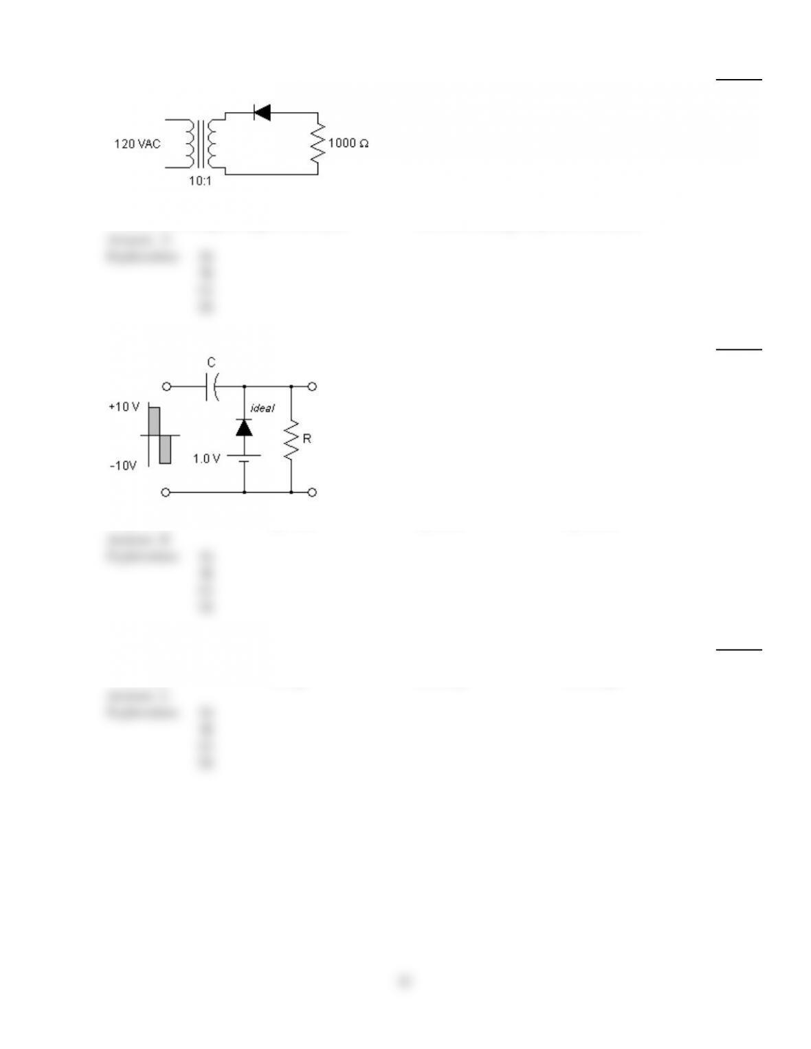
Given that a 1000 Hz signal is applied to a clamper with a resistor value of 10 k. What is the
minimum value of capacitor needed to maintain safe clamping action?
42)
A)
10 pF
B)
5 pF
C)
250 pF
D)
0.25 pF
Answer:
C
Explanation:
A)
B)
C)
D)
12
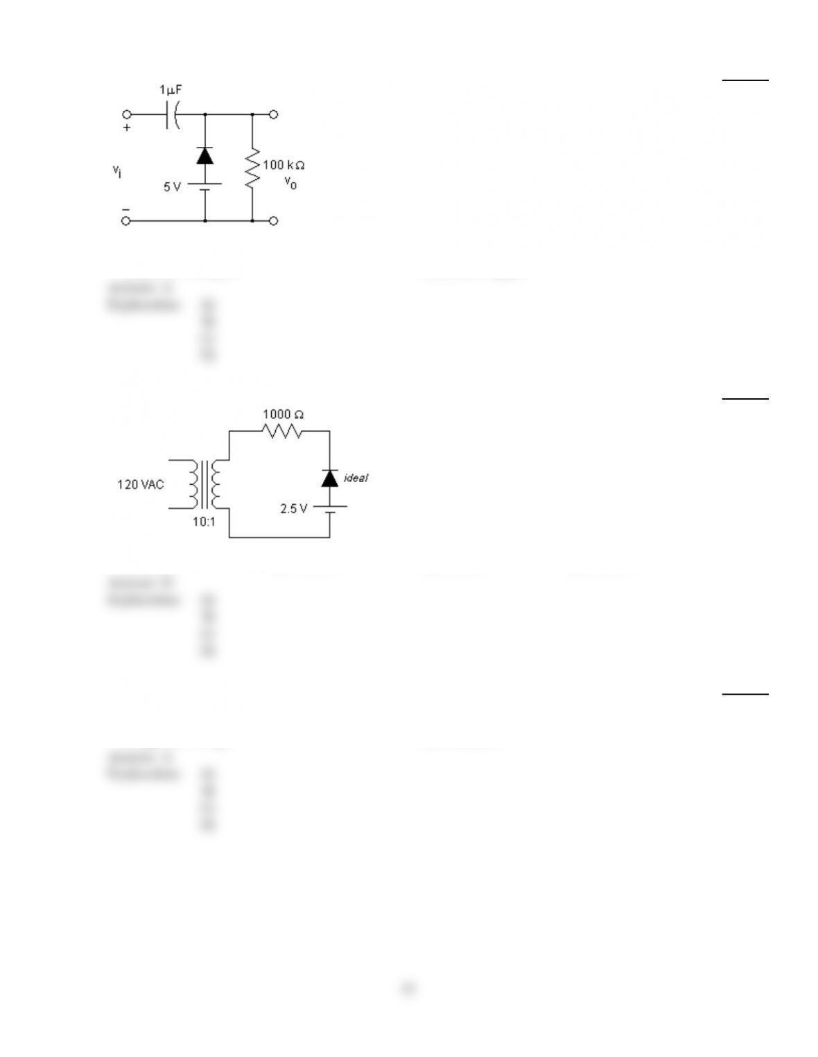
43)
This circuit uses a ________.
43)
A)
negative clamper
B)
negative clipper
C)
positive clamper
D)
positive clipper
Answer:
A
Explanation:
A)
B)
C)
D)
44)
For this clipping circuit, what is the maximum output voltage when the diode is not conducting?
44)
A)
+ 2.5 V
B)
– 16.97 V
C)
+ 19.47 V
D)
+ 16.97 V
Answer:
D
Explanation:
A)
B)
C)
D)
45)
A clamper must have a(n) ________ that is large enough to maintain the capacitor’s charge during
diode conduction.
45)
A)
RC time constant
B)
diode voltage
C)
applied voltage
D)
dc restorer
Answer:
A
Explanation:
A)
B)
C)
D)
13
46)
The Zener diode is on if the applied voltage, V, is ________.
46)
A)
V <VZ
B)
V VZ
C)
V <VZ / 2
D)
V > 2VZ
Answer:
B
Explanation:
A)
B)
C)
D)
47)
The most frequent application for a ________ is in regulator networks and as a reference voltage.
47)
A)
half–wave rectifier
B)
Zener diode
C)
full–wave rectifier
D)
ideal diode
Answer:
B
Explanation:
A)
B)
C)
D)
48)
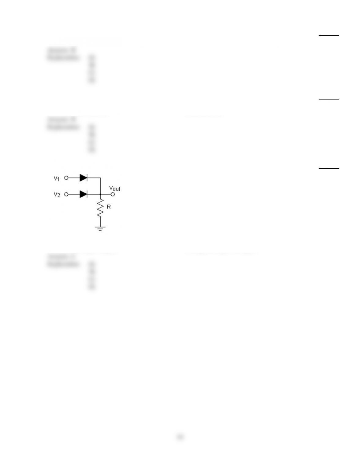
Name the logic gate that is formed by this circuit.
48)
A)
negative logic OR gate
B)
positive logic AND gate
C)
positive logic OR gate
D)
negative logic AND gate
Answer:
C
Explanation:
A)
B)
C)
D)
14
49)
For this clipping circuit, what will be the maximum output voltage when the diode is conducting?
49)
A)
+ 19.47 Volts
B)
+ 16.97 Volts
C)
+ 2.5 Volts
D)
– 16.97 Volts
Answer:
C
Explanation:
A)
B)
C)
D)
50)
When the Zener regulator is used to stabilize the output voltage, given a fixed input voltage and a
variable load resistance, a load resistance that is too small results in ________.
50)
A)
VL being greater than VZ
B)
VL being less than VZ
C)
VZ being equal to Vin
D)
VL being equal to VZ
Answer:
B
Explanation:
A)
B)
C)
D)
15

Answer Key
Testname: C2
1)
C
2)
D
3)
A
4)
D
5)
A
6)
A
7)
D
8)
D
9)
B
10)
C
11)
D
12)
D
13)
C
14)
C
15)
A
16)
D
17)
C
18)
D
19)
A
20)
D
21)
C
22)
D
23)
A
24)
A
25)
A
26)
D
27)
C
28)
C
29)
A
30)
A
31)
A
32)
A
33)
D
34)
C
35)
D
36)
D
37)
A
38)
A
39)
B
40)
A
41)
B
42)
C
43)
A
44)
D
45)
A
46)
B
47)
B
48)
C
49)
C
50)
B