Exam
Name___________________________________
MULTIPLE CHOICE. Choose the one alternative that best completes the statement or answers the question.
1)
An op–amp integrator circuit has a 2 M input resistor and a 5 µF feedback loop capacitor. If the
inverting input voltage is 2 VDC, the final value of the output voltage is ________.
1)
A)
–20 V
B)
–0.2 V
C)
0.02 V
D)
–2 V
Answer:
B
Explanation:
A)
B)
C)
D)
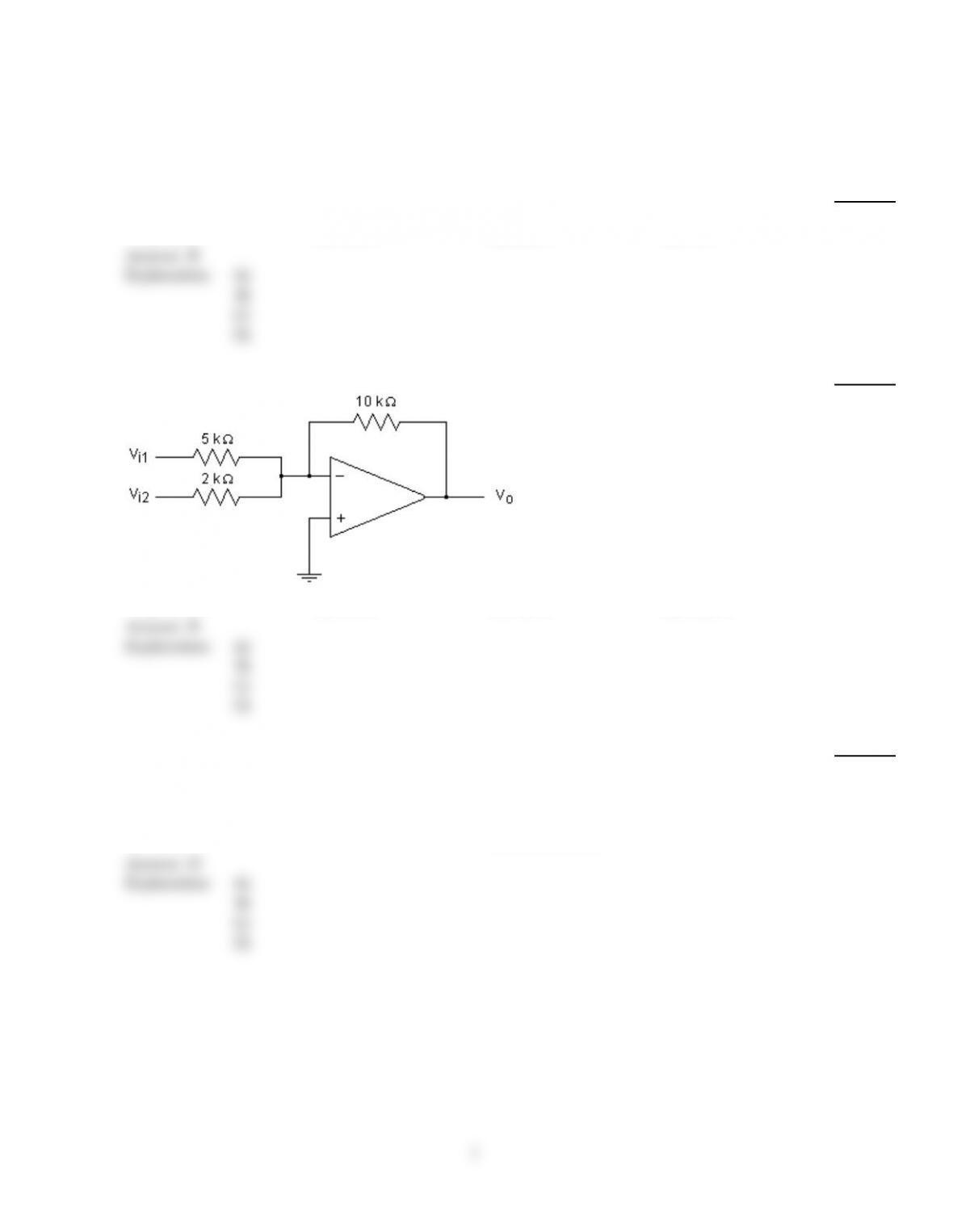
2)
When the input voltages to this circuit are Vi1 = 0.25 V and Vi2 = 0.5 V, the output is ________.
2)
A)
–0.75 V
B)
–3.0 V
C)
–4.5 V
D)
1.125 V
Answer:
B
Explanation:
A)
B)
C)
D)
3)
An inverting amplifier with +11 V supply voltages normally has a sinusoidal output of 10 VPP.
When checking the circuit with an oscilloscope, you find that the output is 0 V. Which of the
following could account for this problem?
3)
A)
RF is shorted by a solder bridge.
B)
R1 is open.
C)
V1= 0
D)
All of the above
Answer:
D
Explanation:
A)
B)
C)
D)
1

4)
An op–amp amplifies only slightly when its ________.
4)
A)
supply voltages are less than +5 V
B)
input offset current is less than 1 mA
C)
input offset voltage is less than 100 mV
D)
inverting or noninverting inputs have a common input
Answer:
D
Explanation:
A)
B)
C)
D)
5)
The operational amplifier will only slightly amplify signals ________.
5)
A)
that are different on both the inputs
B)
when the supply voltages are more then ±25 V
C)
when the supply voltages are less then ±5 V
D)
that are common on both the inputs
Answer:
D
Explanation:
A)
B)
C)
D)
6)
The op–amp circuit that adds each input and multiplies the sum by a fixed amount is called a(n)
________.
6)
A)
unity follower
B)
integrator
C)
summing amplifier
D)
differentiator
Answer:
C
Explanation:
A)
B)
C)
D)
2
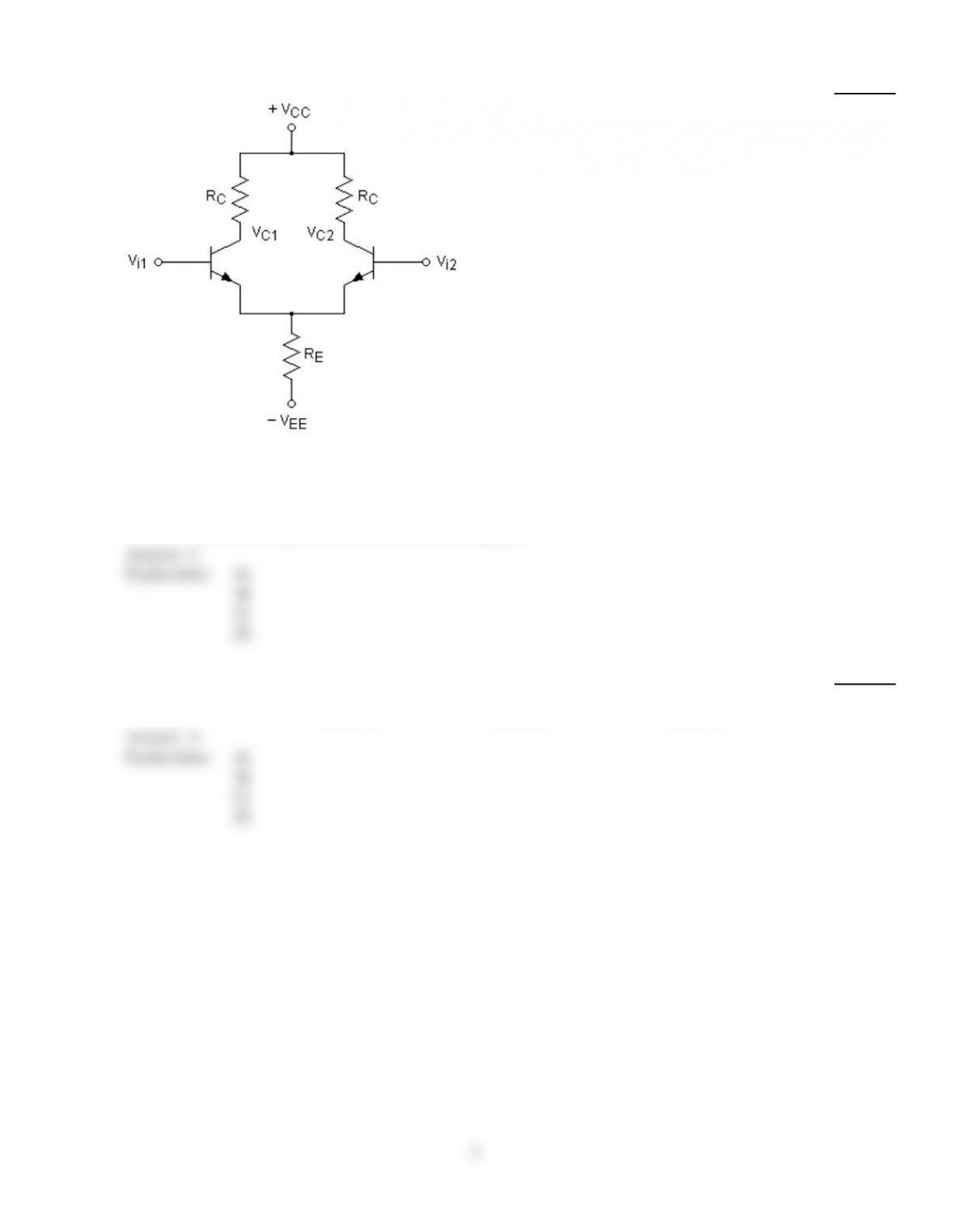
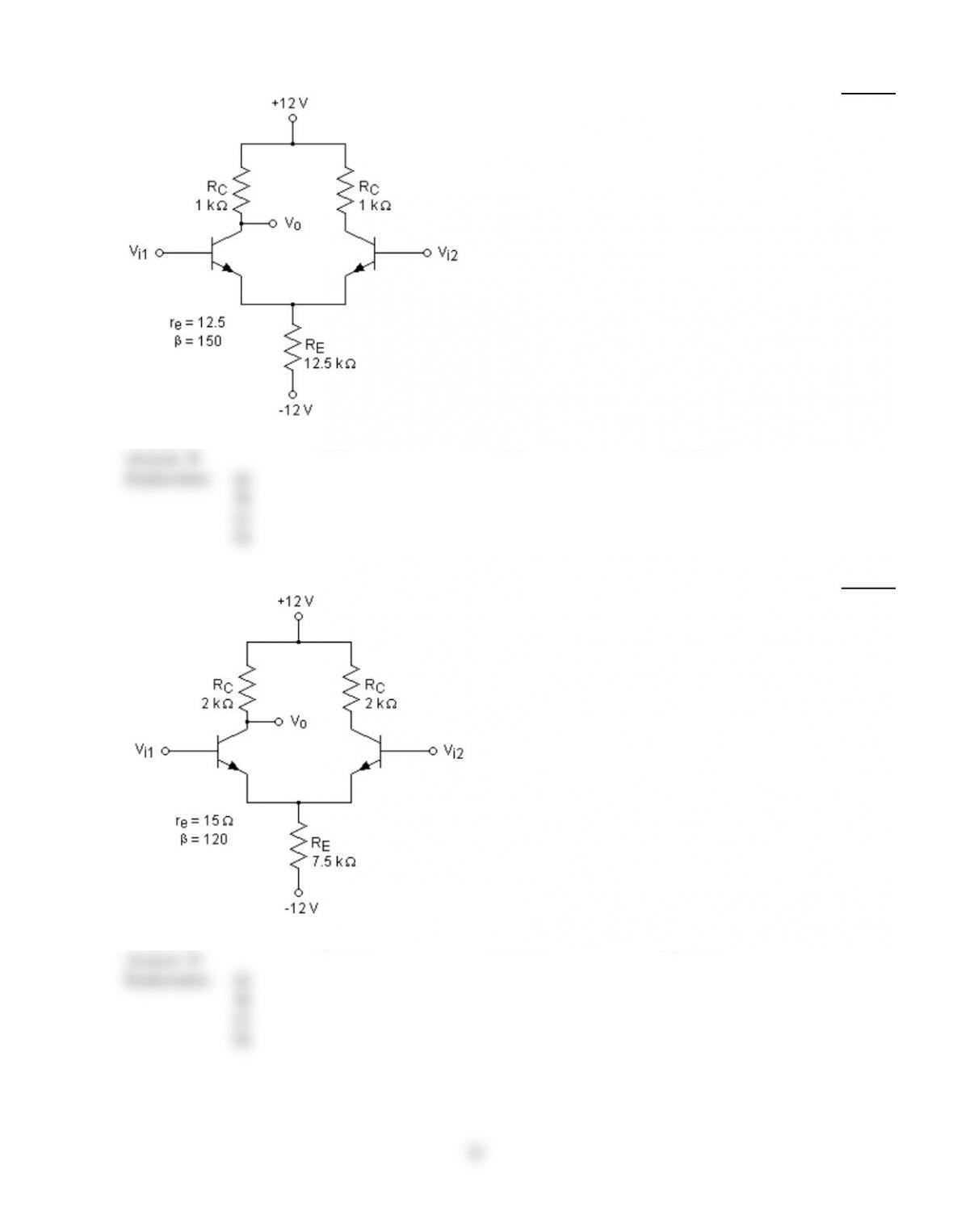
7)
The main features of a differential amplifier, such as the circuit shown here, are ________.
7)
A)
moderate input impedance and very high voltage gain
B)
very high input impedance and moderate voltage gain
C)
very high input impedance and very high voltage gain
D)
moderate input impedance and moderate voltage gain
Answer:
C
Explanation:
A)
B)
C)
D)
8)
Determine the op–amp cutoff–frequency for a device whose unity–gain bandwidth is 1.5 MHz and
the differential–gain is 300 V/mV.
8)
A)
5 Hz
B)
150 Hz
C)
10 Hz
D)
50 Hz
Answer:
A
Explanation:
A)
B)
C)
D)
3

9)
For this AC equivalent circuit of an op–amp, the input signal is applied between the input
terminals and sees an input impedance Ri. This impedance ________.
9)
A)
is a few kilo–ohms
B)
is a few hundred kilo–ohms
C)
is a few hundred ohms
D)
depends on the op–amp used. It could be a few hundred ohms to a few hundred kilo–ohms
Answer:
B
Explanation:
A)
B)
C)
D)
10)
Slew rate is the ________.
10)
A)
ratio of the change in time to the change in output voltage
B)
maximum rate at which the amplifier input voltage can change
C)
maximum rate at which the op–amp output voltage can change
D)
None of the above
Answer:
C
Explanation:
A)
B)
C)
D)
4
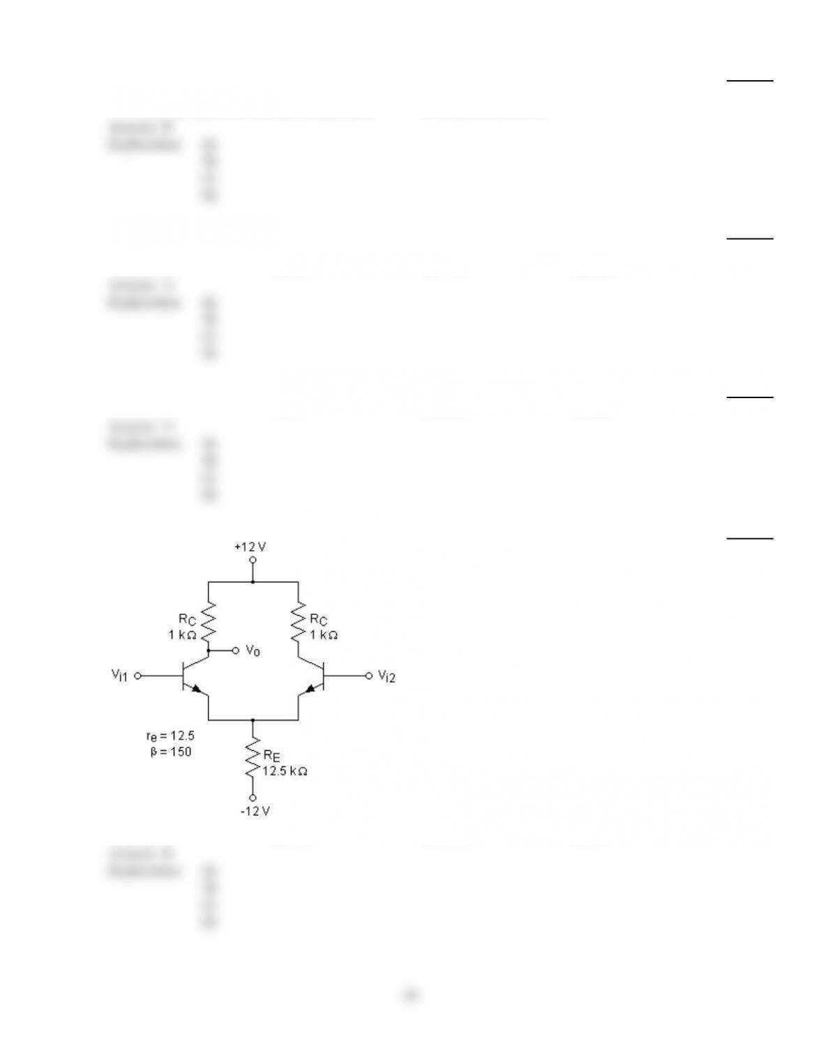
11)
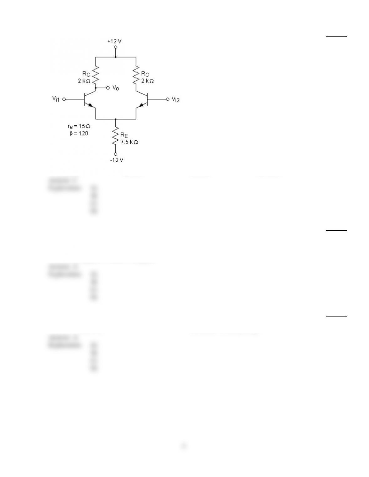
Under single–ended operation the voltage gain for this circuit is ________.
11)
A)
266.66
B)
33.33
C)
66.67
D)
133.33
Answer:
C
Explanation:
A)
B)
C)
D)
12)
The common mode rejection ratio (CMRR) is the ratio of ________.
12)
A)
the difference mode gain to the common mode gain
B)
noninverting gain to inverting gain
C)
the common mode gain to the difference mode gain
D)
inverting gain to noninverting gain
Answer:
A
Explanation:
A)
B)
C)
D)
13)
Op–amps are available in a number of packages. Among the most common forms is the ________.
13)
A)
dual in–line package (DIP)
B)
TO–8 metal can
C)
TO–5 metal can
D)
surface–mount package
Answer:
A
Explanation:
A)
B)
C)
D)
5
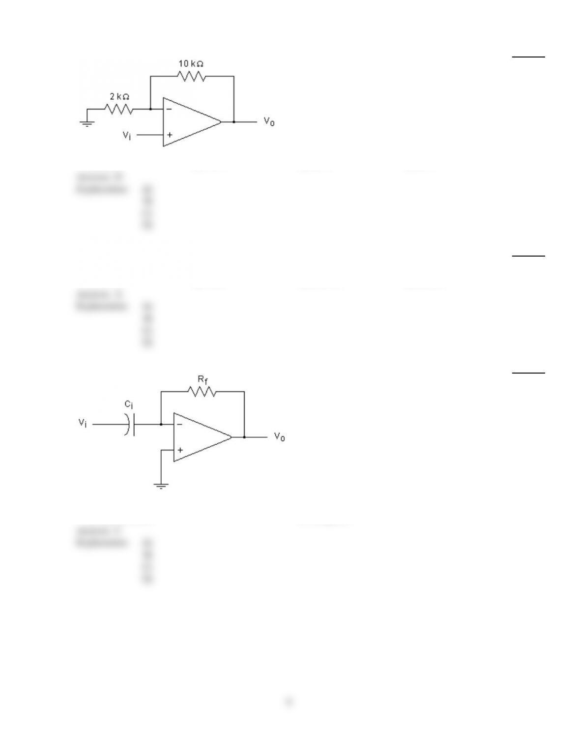
14)
If the input voltage is 0.25 V and the required output voltage is 2.75 V, the value for Rf must be
________.
14)
A)
20.0 k
B)
5.0 k
C)
10.0 k
D)
40.0 k
Answer:
A
Explanation:
A)
B)
C)
D)
15)
When a given op–amp has a common–mode input of 10 V, the output of the device is 1 mV. When
the device has a differential input of 2 mV, the output of the device is 10 V. What is the CMRR of
the device‘?
15)
A)
5000 : 1
B)
5,000,000 : 1
C)
1000 : 1
D)
5 : 1
Answer:
B
Explanation:
A)
B)
C)
D)
16)
If the input voltage is 0.25 V and the output is –2.0 V, the value of Rf must be ________.
16)
A)
16.0 k
B)
5.0 k
C)
10.0 k
D)
40.0 k
Answer:
A
Explanation:
A)
B)
C)
D)
6

17)
The bandwidth of an amplifier is ________.
17)
A)
the range of frequencies between the lower and upper 3 dB frequencies
B)
the range of frequencies over which gain remains relatively constant
C)
the range of frequencies found using f2–f1
D)
All of the above
Answer:
D
Explanation:
A)
B)
C)
D)
18)
A certain inverting op–amp has a closed–loop gain of 50 and a slew rate of 5 V/µsec. What is the
maximum useful frequency of a 2 V input signal applied to this circuit?
18)
A)
5 ×10³ rad/s
B)
100 ×103 rad/s
C)
50 ×103 rad/s
D)
10 ×103 rad/s
Answer:
C
Explanation:
A)
B)
C)
D)
19)
Which of the following statements is true about operational amplifiers?
19)
A)
Op–amps have very high input impedance.
B)
Op–amps have very low output impedance.
C)
Op–amps are very high–gain DC amplifiers.
D)
All of the above
Answer:
D
Explanation:
A)
B)
C)
D)
20)
Op–amp roll–off characteristics are caused by the fact that ________.
20)
A)
an effective compensation circuit is used
B)
they are designed to have high–gain and wide–bandwidth
C)
the uncompensated circuit would be unstable
D)
All of the above
Answer:
D
Explanation:
A)
B)
C)
D)
7
21)
When the input voltage to this circuit is 0.25 V, the output voltage is ________.
21)
A)
10.0 V
B)
3.0 V
C)
5.0 V
D)
1.5 V
Answer:
D
Explanation:
A)
B)
C)
D)
22)
A standard inverting op–amp circuit has an R1 of 10 k and an Rf of 220 k. If the offset voltage is
0.003 V, the Vo(offset) is ________.
22)
A)
69 mV
B)
3 mV
C)
200 mV
D)
6.6 mV
Answer:
A
Explanation:
A)
B)
C)
D)
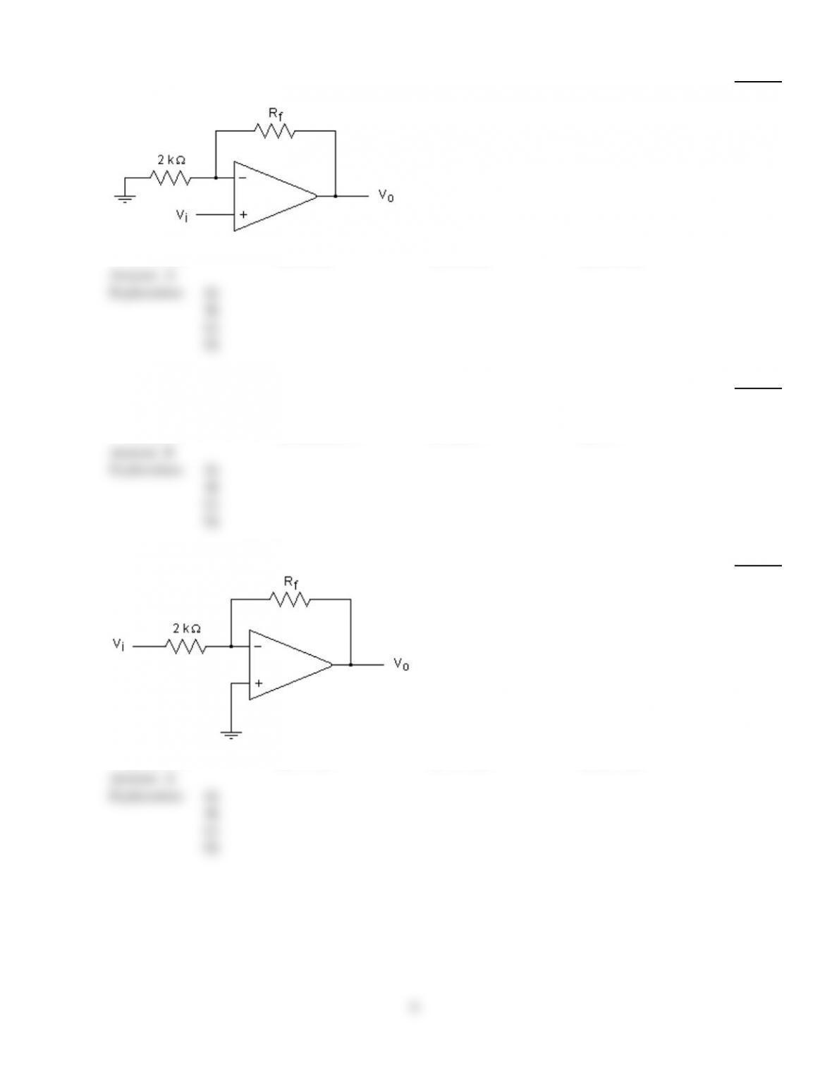
23)
The operational amplifier circuit shown here is a(n) ________.
23)
A)
level comparator
B)
difference amplifier
C)
differentiator
D)
integrator
Answer:
C
Explanation:
A)
B)
C)
D)
8
24)
One basic circuit connection using an op–amp is shown here. If the input voltage is 0.25 V, the
output voltage is ________.
24)
A)
–2.5 V
B)
–1.25 V
C)
–10.0 V
D)
–5.0 V
Answer:
B
Explanation:
A)
B)
C)
D)
25)
The CMRR of an inverting amplifier is always lower than that of its op–amp because ________.
25)
A)
the value of differential gain for an inverting amplifier is lower than that of its op–amp
B)
the common–mode gain of an op–amp increases when it is used in an inverting amplifier
C)
of the lower input impedance of the inverting amplifier
D)
slew–rate limiting decreases the common–mode gain of the op–amp
Answer:
A
Explanation:
A)
B)
C)
D)
26)
The op–amp circuit that has a capacitor as the feedback component is
called a(n) ________.
26)
A)
unity follower
B)
summing amplifier
C)
integrator
D)
differentiator
Answer:
C
Explanation:
A)
B)
C)
D)
27)
Op–amp different iator circuits differ from the integrators in that the differentiators ________.
27)
A)
have a resistor in the feedback loop
B)
are not as useful
C)
have a scale factor of –RC
D)
All of the above
Answer:
D
Explanation:
A)
B)
C)
D)
9
28)
Exceeding the op–amp slew rate results in ________.
28)
A)
improved gain and reduced distortion
B)
clipping and increased distortion
C)
increased power and reduced distortion
D)
None of the above
Answer:
B
Explanation:
A)
B)
C)
D)
29)
An op–amp circuit has ±15 V supply voltages and a voltage gain of 20. The noninverting voltage
(v+) is 0.3 V and the inverting voltage (v–) is 0.35 V. What is the output voltage from the device?
29)
A)
–1 V
B)
+1 V
C)
–7 V
D)
+6 V
Answer:
A
Explanation:
A)
B)
C)
D)
30)
The voltage follower typically has a voltage gain value of ________.
30)
A)
1
B)
10
C)
1000
D)
100
Answer:
A
Explanation:
A)
B)
C)
D)
31)
13. Under common–mode operation, the common–mode voltage gain for this circuit is ________.
31)
A)
40
B)
0.08
C)
0.0397
D)
80
Answer:
B
Explanation:
A)
B)
C)
D)
10
32)
When calculating the total offset voltage the absolute values are used to accommodate the fact that
________.
32)
A)
offset voltage can be negative or positive
B)
offset current can be negative or positive
C)
both the offset current and voltage can be negative or positive
D)
None of the above
Answer:
C
Explanation:
A)
B)
C)
D)
33)
The double–ended voltage gain for this circuit is ________.
33)
A)
66.66
B)
0.266
C)
133.33
D)
0.133
Answer:
C
Explanation:
A)
B)
C)
D)
11
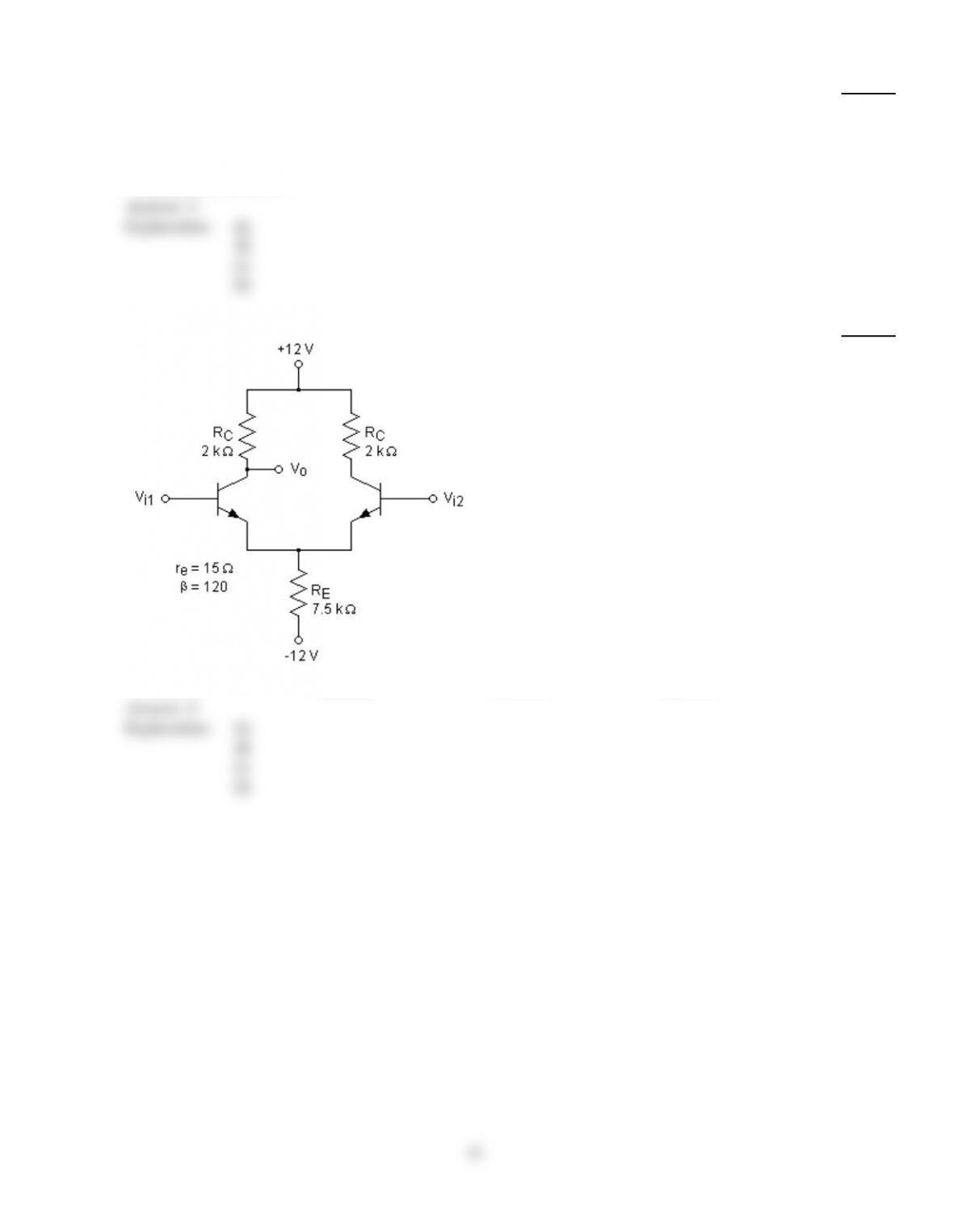
34)
The double–ended voltage gain for this circuit is ________.
34)
A)
0.08
B)
80
C)
40
D)
0.0397
Answer:
B
Explanation:
A)
B)
C)
D)
35)
Under common–mode operation, the common–mode voltage gain is ________.
35)
A)
0.266
B)
66.66
C)
33.33
D)
0.133
Answer:
D
Explanation:
A)
B)
C)
D)
12

36)
An inverting amplifier and a noninverting amplifier are built using the same values of Rf and R1.
Assuming that the op–amps being used in the two circuits have identical common–mode gain
values, ________.
36)
A)
the inverting amplifier has the higher CMRR
B)
the CMRR is the same for the inverting and noninverting amplifiers
C)
the noninverting amplifier has the higher CMRR
D)
None of the above
Answer:
C
Explanation:
A)
B)
C)
D)
37)
Op–amp output offset voltage can be totally explained by ________.
37)
A)
the external circuit connection components
B)
the input offset voltage
C)
input offset current
D)
None of the above
Answer:
D
Explanation:
A)
B)
C)
D)
38)
A standard inverting op–amp circuit has an R1 of 10 k and an Rf of 220 k. If the offset current is
100 nA the output offset voltage due to this current is ________.
38)
A)
10 mV
B)
8 mV
C)
22 mV
D)
32 mV
Answer:
C
Explanation:
A)
B)
C)
D)
39)
The inverting and noninverting inputs to an op–amp are used to drive a(n) ________ amplifier.
39)
A)
differential
B)
noninverting
C)
open–loop
D)
inverting
Answer:
A
Explanation:
A)
B)
C)
D)
13
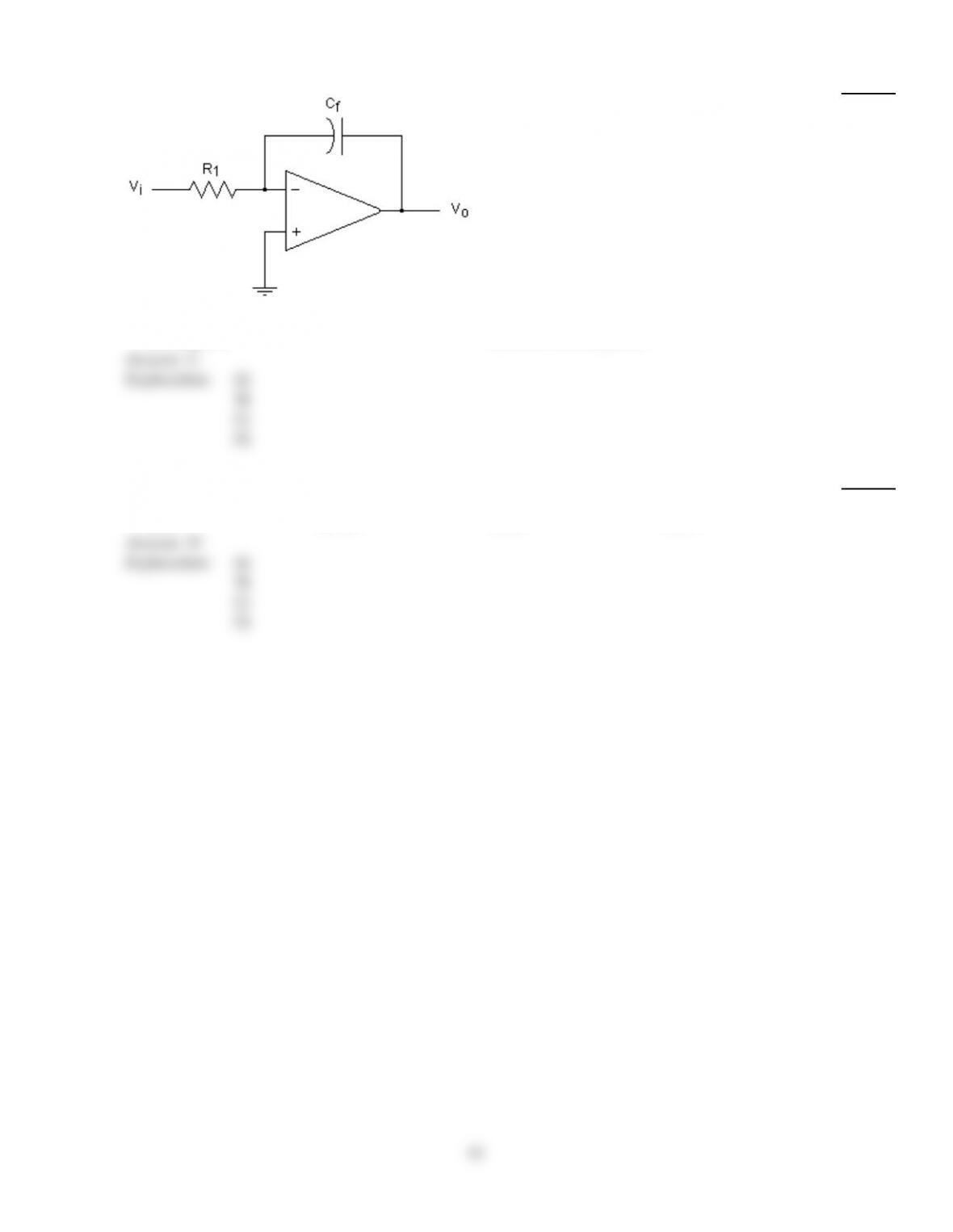
40)
The operational amplifier circuit shown here is a(n) ________.
40)
A)
different iator
B)
level comparator
C)
integrator
D)
difference amplifier
Answer:
C
Explanation:
A)
B)
C)
D)
41)
A certain op–amp has a slew rate of 4 V/µsec. What is the maximum closed–loop voltage gain if the
input voltage rises at a rate of 5 V/l00 µsec?
41)
A)
40
B)
200
C)
20
D)
80
Answer:
D
Explanation:
A)
B)
C)
D)
14
42)
Under single–ended operation, the voltage gain for this is ________.
42)
A)
160
B)
40
C)
80
D)
20
Answer:
B
Explanation:
A)
B)
C)
D)
43)
A summing integrator is an op–amp integrator that has ________.
43)
A)
multiple input resistors
B)
multiple input resistors and feedback capacitors
C)
multiple feedback capacitors
D)
None of the above
Answer:
A
Explanation:
A)
B)
C)
D)
15

Answer Key
Testname: C10
1)
B
2)
B
3)
D
4)
D
5)
D
6)
C
7)
C
8)
A
9)
B
10)
C
11)
C
12)
A
13)
A
14)
A
15)
B
16)
A
17)
D
18)
C
19)
D
20)
D
21)
D
22)
A
23)
C
24)
B
25)
A
26)
C
27)
D
28)
B
29)
A
30)
A
31)
B
32)
C
33)
C
34)
B
35)
D
36)
C
37)
D
38)
C
39)
A
40)
C
41)
D
42)
B
43)
A