26)
Which of the following is not an application of an analog MOSFET switch?
26)
A)
Analog multiplexer
B)
Sample–and–hold circuit
C)
Inverter
D)
Switched capacitor circuit
Answer:
C
Explanation:
A)
B)
C)
D)
27)
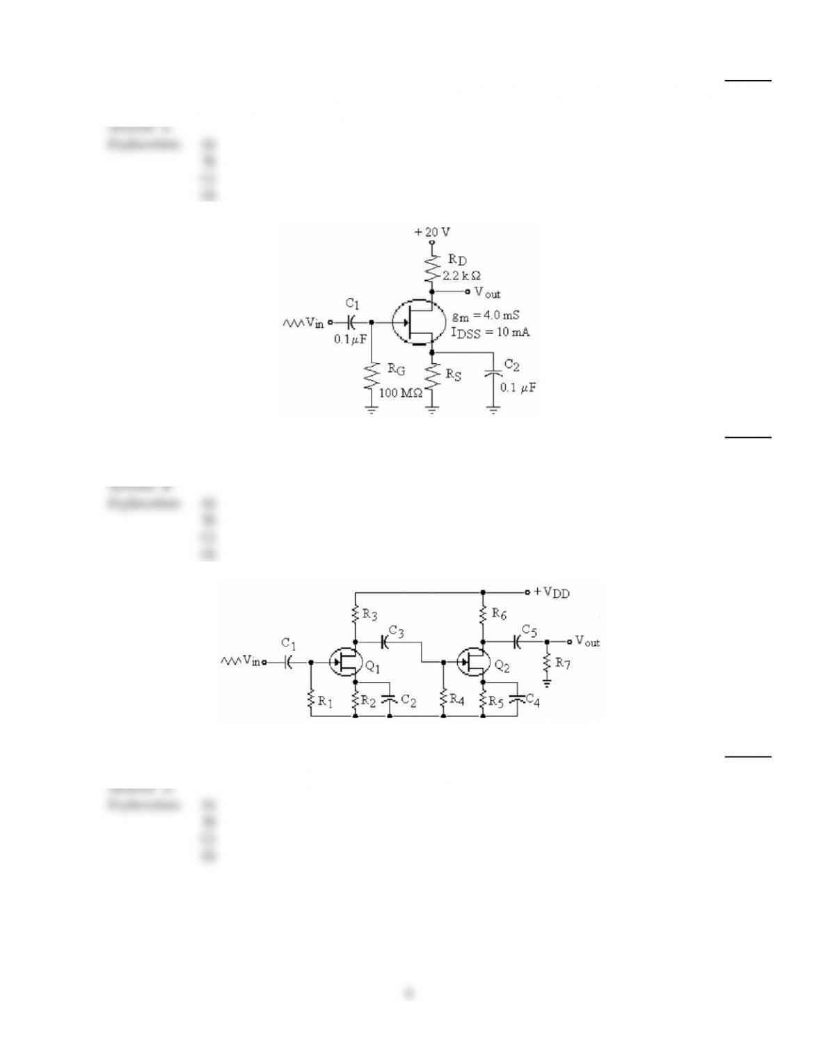
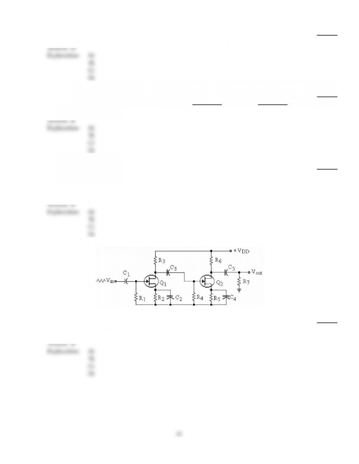
Refer to the figure above. If Vin = 1 Vp–p, the output voltage Vout would be
27)
A)
clipped on the negative peaks.
B)
undistorted.
C)
clipped on the positive peaks.
D)
0 V.
Answer:
B
Explanation:
A)
B)
C)
D)
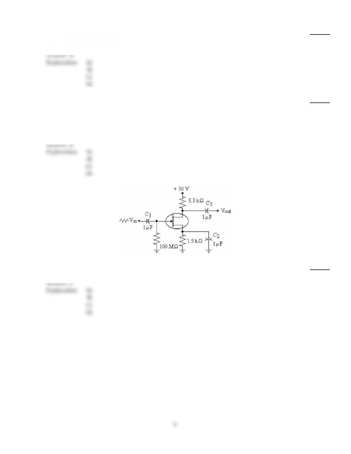
28)
Refer to the figure above. If AV1 = 18 and AVt = 288, the value of AV2 would be
28)
A)
16.
B)
5184.
C)
18.
D)
49.18.
Answer:
A
Explanation:
A)
B)
C)
D)
8
29)
Refer to the figure above. If R3 opened, Vout would
29)
A)
increase.
B)
decrease.
C)
remain the same.
D)
distort.
Answer:
B
Explanation:
A)
B)
C)
D)
30)
When troubleshooting a multiple stage CS amplifier, signal tracing reveals a significant amount of
signal voltage at the source of the first stage. The most likely problem is
30)
A)
a shorted load in third stage.
B)
an open source bypass capacitor.
C)
too much dc supply voltage.
D)
an open coupling capacitor from signal source.
Answer:
B
Explanation:
A)
B)
C)
D)
31)
Refer to the figure above. If ID= 4 mA, IDSS = 16 mA, and VGS(off) = – 8 V, VDS would be
31)
A)
30 V.
B)
19.2 V.
C)
10.8 V.
D)
–6 V.
Answer:
C
Explanation:
A)
B)
C)
D)
9
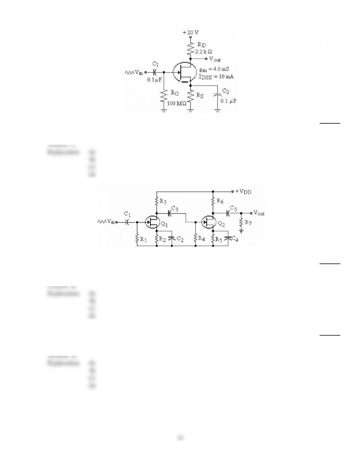
32)
Refer to the figure above. If R5 opened, Vout would
32)
A)
increase.
B)
decrease.
C)
remain the same.
D)
distort.
Answer:
D
Explanation:
A)
B)
C)
D)
33)
Two FET amplifiers operated in cascade have gains of 6 dB and 8 dB. The total overall gain in dB is
33)
A)
14 dB.
B)
64 dB.
C)
2 dB.
D)
48 dB.
Answer:
A
Explanation:
A)
B)
C)
D)
34)
Approximately how much signal voltage should be measured at the bypassed source of a common
source amplifier?
34)
A)
the same amount as the drain
B)
Vin
C)
Vin
2
D)
0 V
Answer:
D
Explanation:
A)
B)
C)
D)
10
35)
Refer to the figure above. Assuming midpoint biasing, if VGS = – 4 V, the value of RS that will
provide this value is
35)
A)
600 .
B)
1.2 k.
C)
800 .
D)
80 .
Answer:
C
Explanation:
A)
B)
C)
D)
36)
Refer to the figure above. If C5 opened, the signal voltage across R7 would
36)
A)
increase.
B)
be zero.
C)
remain the same.
D)
distort.
Answer:
B
Explanation:
A)
B)
C)
D)
37)
When the input signal is large, a source follower has
37)
A)
a small distortion.
B)
a high input resistance.
C)
a voltage gain of less than one.
D)
All of the above.
Answer:
D
Explanation:
A)
B)
C)
D)
11
38)
A common–source amplifier has a ________ phase shift between the input and the output.
38)
A)
90°
B)
360°
C)
45°
D)
180°
Answer:
D
Explanation:
A)
B)
C)
D)
39)
A CS amplifier has a voltage gain of
39)
A)
gmRs.
B)
gmRd.
C)
gmRd
(1 + gmRd).
D)
gmRs
(1 + gmRd).
Answer:
B
Explanation:
A)
B)
C)
D)
40)
The main reason that the input resistance of FET amplifiers is so high is that the
40)
A)
FET junctions are forward–biased and made of germanium.
B)
gate junction is reverse–biased.
C)
power supplies used are high voltage/low current.
D)
biasing resistors are extremely small.
Answer:
B
Explanation:
A)
B)
C)
D)
41)
Refer to the figure above. If C2 opened, Vout would
41)
A)
increase.
B)
decrease.
C)
remain the same.
D)
distort.
Answer:
B
Explanation:
A)
B)
C)
D)
12

42)
If RS is not bypassed,
42)
A)
the dc power supply will have excessive ripple.
B)
the gain will be reduced.
C)
no signal will be coupled to the output.
D)
the gain will be extremely high.
Answer:
B
Explanation:
A)
B)
C)
D)
43)
The capacitor connected to the source of a common source amplifier
43)
A)
makes the source an ac ground point.
B)
is used for input coupling.
C)
is needed for extra power supply filtering.
D)
is used for output coupling.
Answer:
A
Explanation:
A)
B)
C)
D)
TRUE/FALSE. Write ‘T’ if the statement is true and ‘F’ if the statement is false.
44)
An analog MOSFET switch is turned on when the gate receives a positive voltage pulse.
44)
Answer:
True
False
Explanation:
45)
The formula for the voltage gain of a common–source amplifier is RD/gm.
45)
Answer:
True
False
Explanation:
46)
FETs are superior to BJTs in almost all switching applications.
46)
Answer:
True
False
Explanation:
47)
The addition of a source bypass capacitor will increase the voltage gain.
47)
Answer:
True
False
Explanation:
48)
In an amplifier using a JFET, the gate current is approximately 0.
48)
Answer:
True
False
Explanation:
49)
Cascode amplifiers are used primarily in radio frequency applications.
49)
Answer:
True
False
Explanation:
13

50)
A MOSFET switch is turned on and off by changing the source voltage.
50)
Answer:
True
False
Explanation:
51)
A pulse–width–modulator employs a square–wave generator and a comparator.
51)
Answer:
True
False
Explanation:
52)
The 3 stages in a class D amplifier are the pulse–width–modulator, the switching amplifier, and the
low–pass filter.
52)
Answer:
True
False
Explanation:
53)
Most of the gain in a JFET–based cascode amplifier is provided by the CS amplifier.
53)
Answer:
True
False
Explanation:
54)
FET amplifiers generally have lower distortion than BJT amplifiers.
54)
Answer:
True
False
Explanation:
55)
Class D amplifiers usually employ JFETs.
55)
Answer:
True
False
Explanation:
56)
CMOS combines n–channel and p–channel D–MOSFETs.
56)
Answer:
True
False
Explanation:
57)
Load resistance added to the output of an amplifier increases the voltage gain.
57)
Answer:
True
False
Explanation:
58)
Power MOSFETs have a negative temperature coefficient and therefore are less prone to thermal
runaway.
58)
Answer:
True
False
Explanation:
14