Exam
Name___________________________________
MULTIPLE CHOICE. Choose the one alternative that best completes the statement or answers the question.
1)
How much dc voltage should always be measured at the gate of a common–gate amplifier?
1)
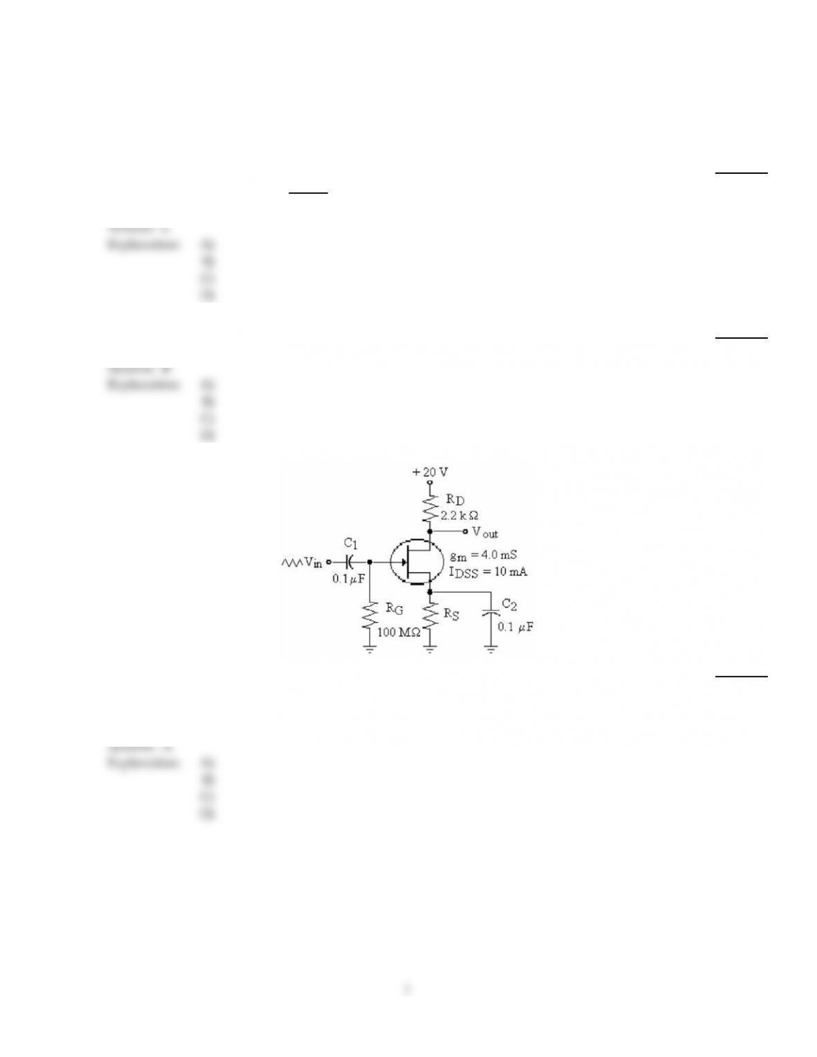
A)
+VDD
B)
+VDD
2
C)
0 V
D)
0.7 V
Answer:
C
Explanation:
A)
B)
C)
D)
2)
Where is the input signal applied in a common–gate amplifier?
2)
A)
Base
B)
Source
C)
Drain
D)
Gate
Answer:
B
Explanation:
A)
B)
C)
D)
3)
Refer to the figure above. If the measured value of Vout were below normal, the problem might be
that
3)
A)
C2 is open.
B)
Vin has increased.
C)
RD is open.
D)
C2 is shorted.
Answer:
A
Explanation:
A)
B)
C)
D)
1
4)
A source follower has a voltage gain of
4)
A)
gmRd
(1 + gmRd).
B)
gmRd.
C)
gmRs
(1 + gmRS).
D)
gm
RS.
Answer:
C
Explanation:
A)
B)
C)
D)
5)
Changing ________ can control the voltage gain of a common–source amplifier.
5)
A)
the input voltage
B)
VDD
C)
gm
D)
RS
Answer:
C
Explanation:
A)
B)
C)
D)
6)
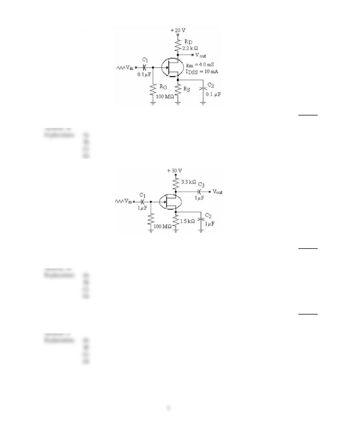
Refer to the figure above. If gm= 4000 µS and a signal of 75 mV rms is applied to the gate, the p–p
output voltage is
6)
A)
990 Vp–p.
B)
990 mV.
C)
2.8 Vp–p.
D)
1.13 Vp–p.
Answer:
C
Explanation:
A)
B)
C)
D)
7)
In a self–biased common–source amplifier, what purpose does resistor RG serve?
7)
A)
Prevents loading of the ac signal source
B)
Develops the gate–source bias current
C)
Keeps the gate at approximately zero volts
D)
Both A and C above.
Answer:
D
Explanation:
A)
B)
C)
D)
2
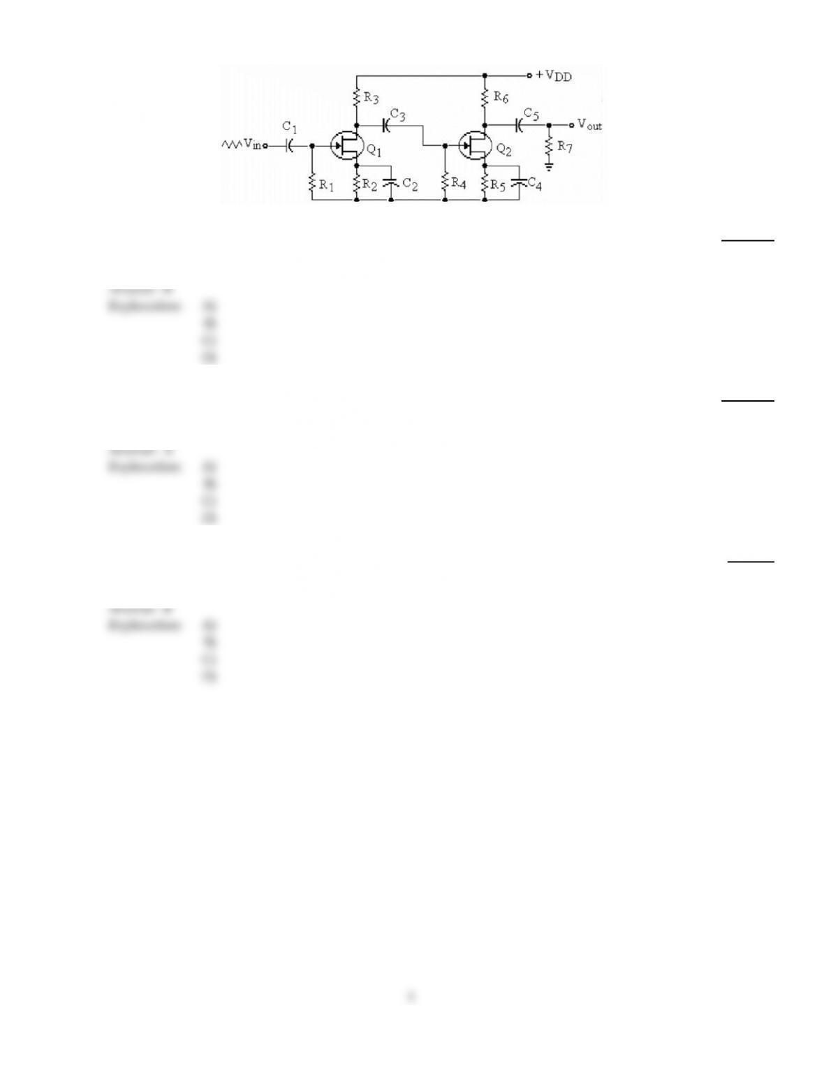
8)
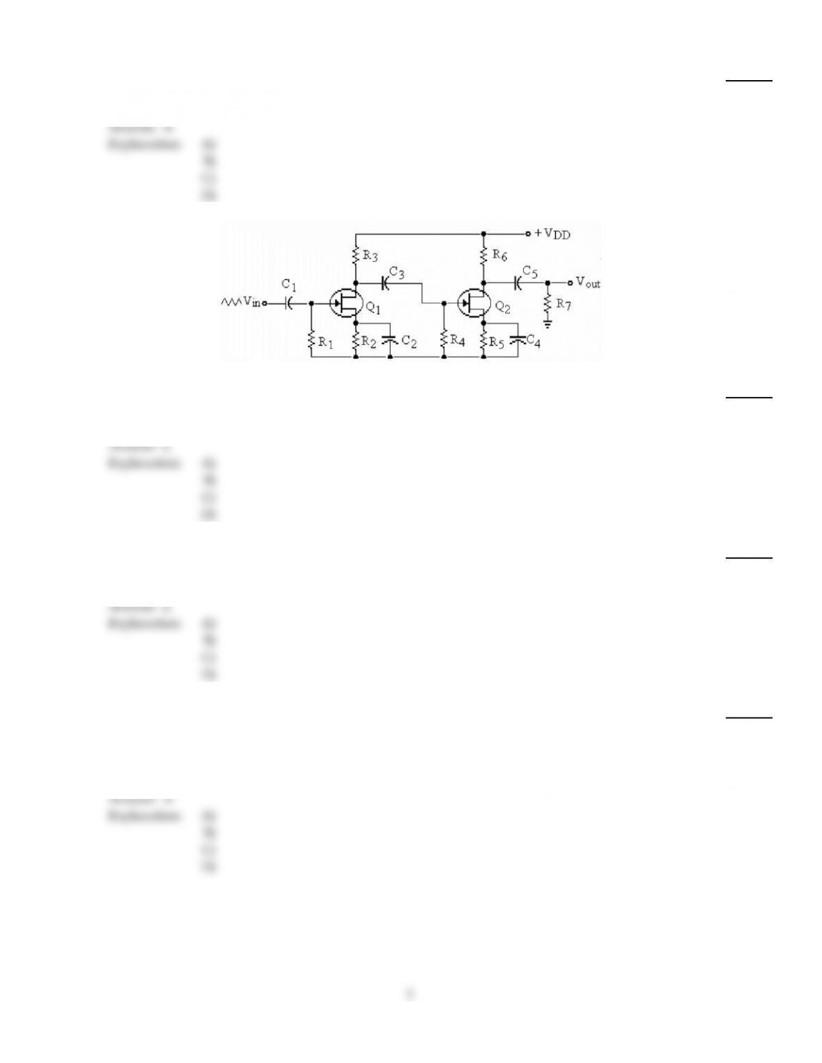
Refer to the figure above. If the source–drain of Q2 shorted, the output signal from Q1 would
8)
A)
increase.
B)
decrease.
C)
remain the same.
D)
distort.
Answer:
B
Explanation:
A)
B)
C)
D)
9)
Refer to the figure above. If R7 were to increase in value, Vout would
9)
A)
increase.
B)
decrease.
C)
remain the same.
D)
distort.
Answer:
A
Explanation:
A)
B)
C)
D)
10)
Two common–source amplifiers are cascaded. The overall phase shift from the input of the first
amplifier to the output of the second amplifier is
10)
A)
180°.
B)
0°.
C)
45°.
D)
90°.
Answer:
B
Explanation:
A)
B)
C)
D)
3
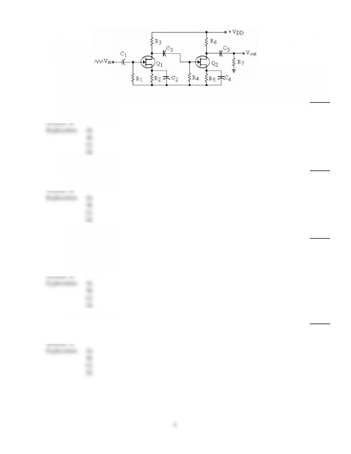
11)
Refer to the figure above. If C3 opened, Vout would
11)
A)
increase.
B)
decrease.
C)
remain the same.
D)
distort.
Answer:
B
Explanation:
A)
B)
C)
D)
12)
Two FET amplifiers are operated in cascade. If the gain of the amplifiers is equal and the total
overall gain is 25, the gain of each amplifier is
12)
A)
7.25.
B)
5.
C)
2.
D)
12.5.
Answer:
B
Explanation:
A)
B)
C)
D)
13)
The ac equivalent circuit of a FET amplifier assumes that the capacitors
13)
A)
have an XC of 600 at the signal frequency.
B)
have an XC of 1 M at the signal frequency.
C)
are treated like opens.
D)
are treated like shorts.
Answer:
D
Explanation:
A)
B)
C)
D)
14)
Which of the following is not a characteristic of a JFET–based cascode amplifier?
14)
A)
High input capacitance
B)
High gain
C)
High input resistance
D)
High frequency response
Answer:
A
Explanation:
A)
B)
C)
D)
4
15)
Which of the following is not part of a class D amplifier?
15)
A)
Oscillator
B)
Switching amplifier
C)
Pulse–width modulator
D)
Low–pass filter
Answer:
A
Explanation:
A)
B)
C)
D)
16)
Refer to the figure above. If R1 opened, Vout would
16)
A)
increase.
B)
decrease.
C)
remain the same.
D)
distort.
Answer:
C
Explanation:
A)
B)
C)
D)
17)
Refer to the figure above. If C4 opened, the signal voltage at the drain of Q1 would
17)
A)
increase.
B)
decrease.
C)
remain the same.
D)
distort.
Answer:
C
Explanation:
A)
B)
C)
D)
18)
What is the role of the low–pass filter in a class D amplifier?
18)
A)
Remove the modulating frequency and harmonics
B)
Prevent oscillation
C)
Limit amplifier frequency response
D)
Remove hum
Answer:
A
Explanation:
A)
B)
C)
D)
5
19)
Refer to the figure above. If ID= 6 mA, the value of VGS is
19)
A)
–19.8 V.
B)
–10.2 V.
C)
–9 V.
D)
9 V.
Answer:
C
Explanation:
A)
B)
C)
D)
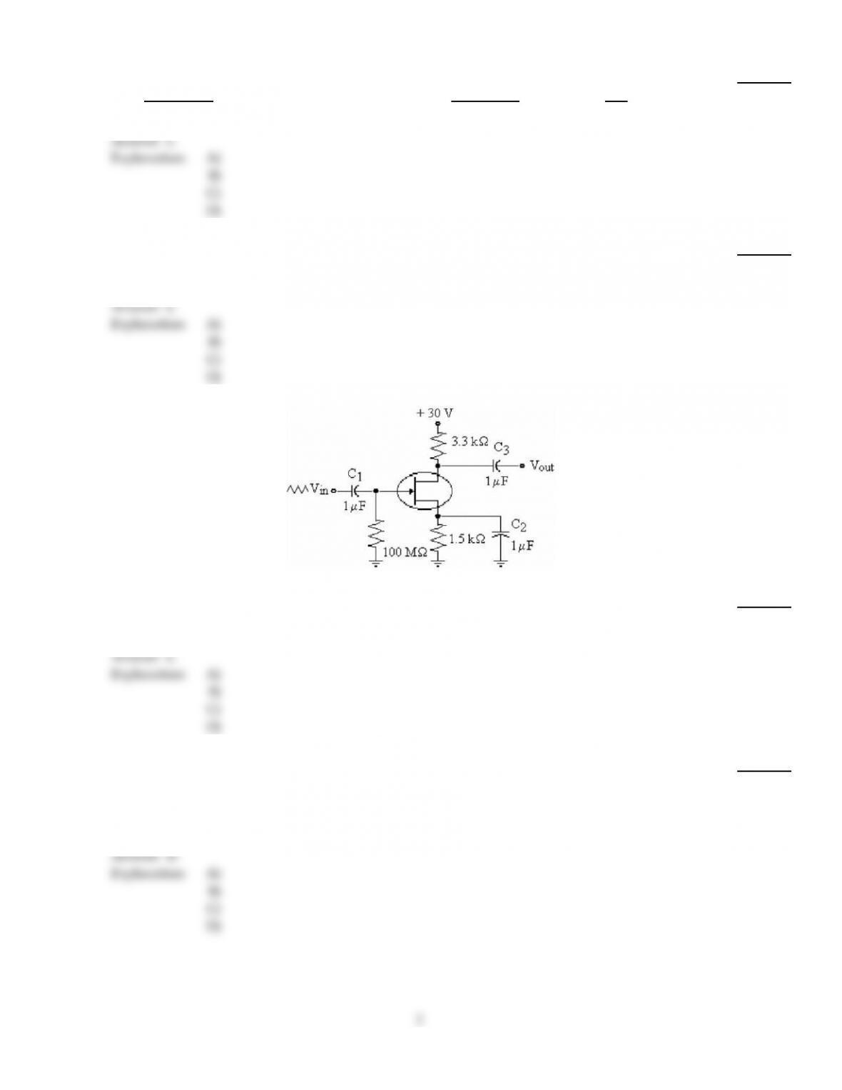
20)
Refer to the figure above. If gm= 6500 µS and an input signal of 125 mVp–p is applied to the gate,
the output voltage Vout is
20)
A)
0.8125 Vp–p.
B)
6.25 Vp–p.
C)
1.625 Vp–p.
D)
2.68 Vp–p.
Answer:
D
Explanation:
A)
B)
C)
D)
21)
What component of an FET amplifier needs to be at least ten times greater than RD to ensure
maximum voltage gain?
21)
A)
Rs
B)
gm
C)
RS
D)
r‘ds
Answer:
D
Explanation:
A)
B)
C)
D)
22)
If the interstage coupling capacitor opens in a two stage FET amplifier, the output signal will
22)
A)
be slightly decreased.
B)
double in amplitude.
C)
be slightly increased.
D)
be zero.
Answer:
D
Explanation:
A)
B)
C)
D)
6
23)
Refer to the figure above. If Vin = 50 mVp–p, the output voltage is
23)
A)
0.044 Vp–p.
B)
440 mVp–p.
C)
50 mVp–p.
D)
4.4 Vp–p.
Answer:
B
Explanation:
A)
B)
C)
D)
24)
Refer to the figure above. If C2 opened, the output signal would
24)
A)
decrease and then increase.
B)
not change.
C)
increase in value.
D)
decrease in value.
Answer:
D
Explanation:
A)
B)
C)
D)
25)
Which of the following is not a FET amplifier?
25)
A)
Common–gate
B)
Source–follower
C)
Emitter–follower
D)
Common–drain
Answer:
C
Explanation:
A)
B)
C)
D)
7