24)
Special handling precautions should be taken when working with MOSFETs. Which of the
following is not one of these precautions?
24)
A)
MOSFET devices should have their leads shorted together for shipment and storage.
B)
All test equipment should be grounded.
C)
Workers handling MOSFET devices should not have grounding straps attached to their
wrists.
D)
Never remove or insert MOSFET devices with the power on.
Answer:
C
Explanation:
A)
B)
C)
D)
25)
A JFET manufacturer’s data sheet specifies VGS(off) = – 8 V and IDSS = 6 mA. When VGS = – 4 V,
the value of ID would be
25)
A)
1.5 mA.
B)
4 mA.
C)
1.25 mA.
D)
6 mA.
Answer:
A
Explanation:
A)
B)
C)
D)
26)
The depletion–mode MOSFET can
26)
A)
operate with only negative gate voltages.
B)
not operate in the ohmic region.
C)
operate with positive as well as negative gate voltages.
D)
operate with only positive gate voltages.
Answer:
C
Explanation:
A)
B)
C)
D)
27)
A self–biased n-channel JFET has a VD= 8 V, VGS = – 5 V. The value of VDS is
27)
A)
–5 V.
B)
3 V.
C)
–3 V.
D)
8 V.
Answer:
B
Explanation:
A)
B)
C)
D)
28)
An IGBT has the output characteristics of a ________ but is ________ –controlled like a MOSFET.
28)
A)
BJT, current
B)
FET, voltage
C)
BJT, voltage
D)
FET, current
Answer:
C
Explanation:
A)
B)
C)
D)
7
29)
The channel width in a JFET is controlled by
29)
A)
varying drain voltage.
B)
increasing reverse bias on the drain–source junction.
C)
varying gate voltage.
D)
increasing forward bias on the gate–source junction.
Answer:
C
Explanation:
A)
B)
C)
D)
30)
JFETs are often called
30)
A)
unipolar devices.
B)
bipolar devices.
C)
two–way switches.
D)
one–way switches.
Answer:
A
Explanation:
A)
B)
C)
D)
31)
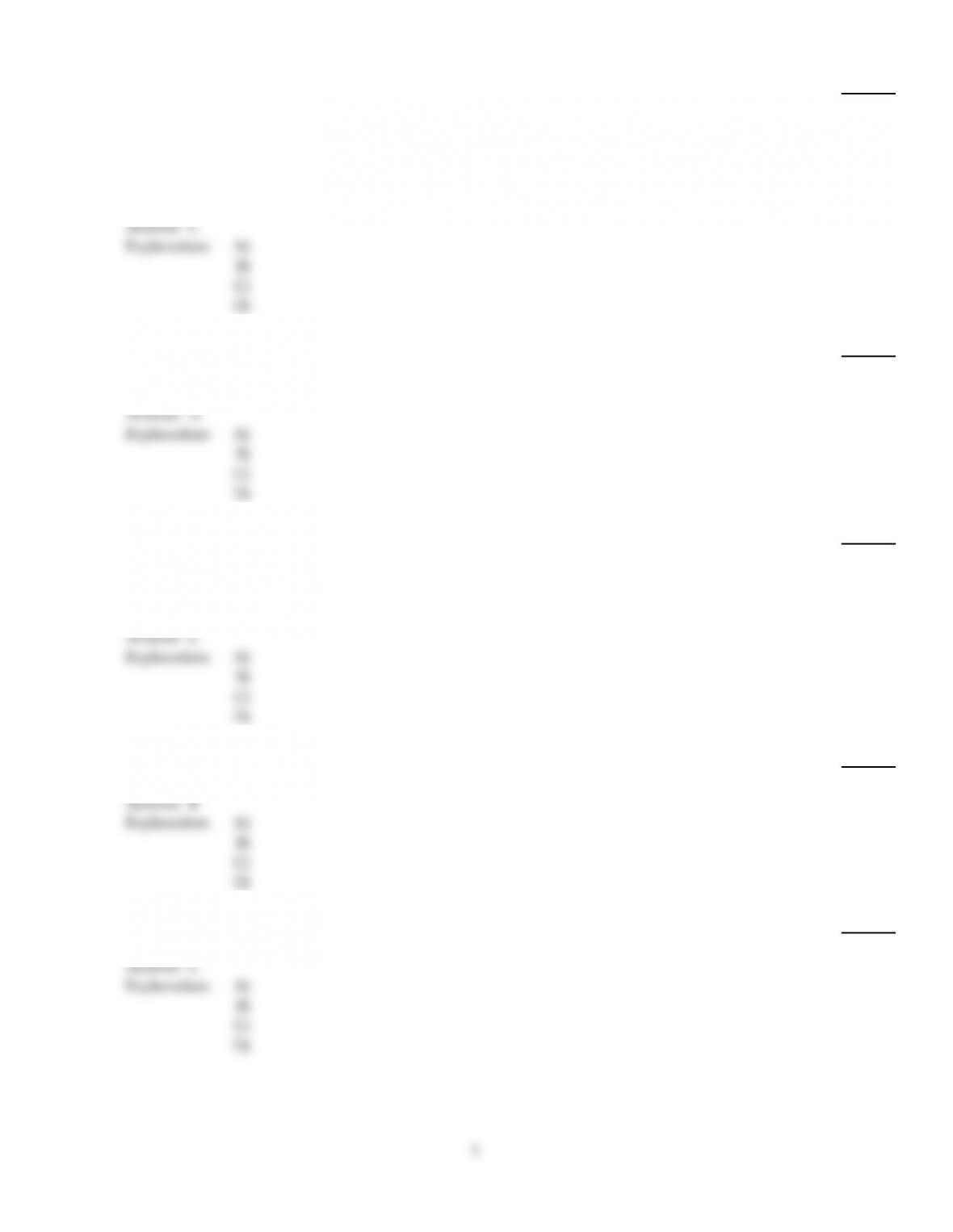
Refer to (a) in the figure above. If ID= 4 mA, the value of VDS is
31)
A)
0 V.
B)
8 V.
C)
12 V.
D)
4 V.
Answer:
B
Explanation:
A)
B)
C)
D)
8
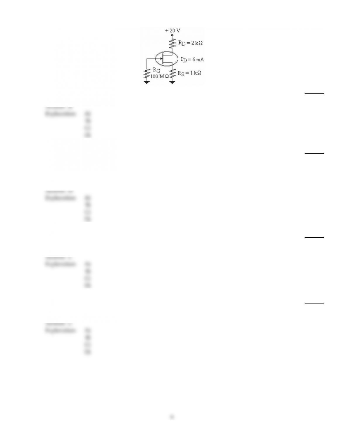
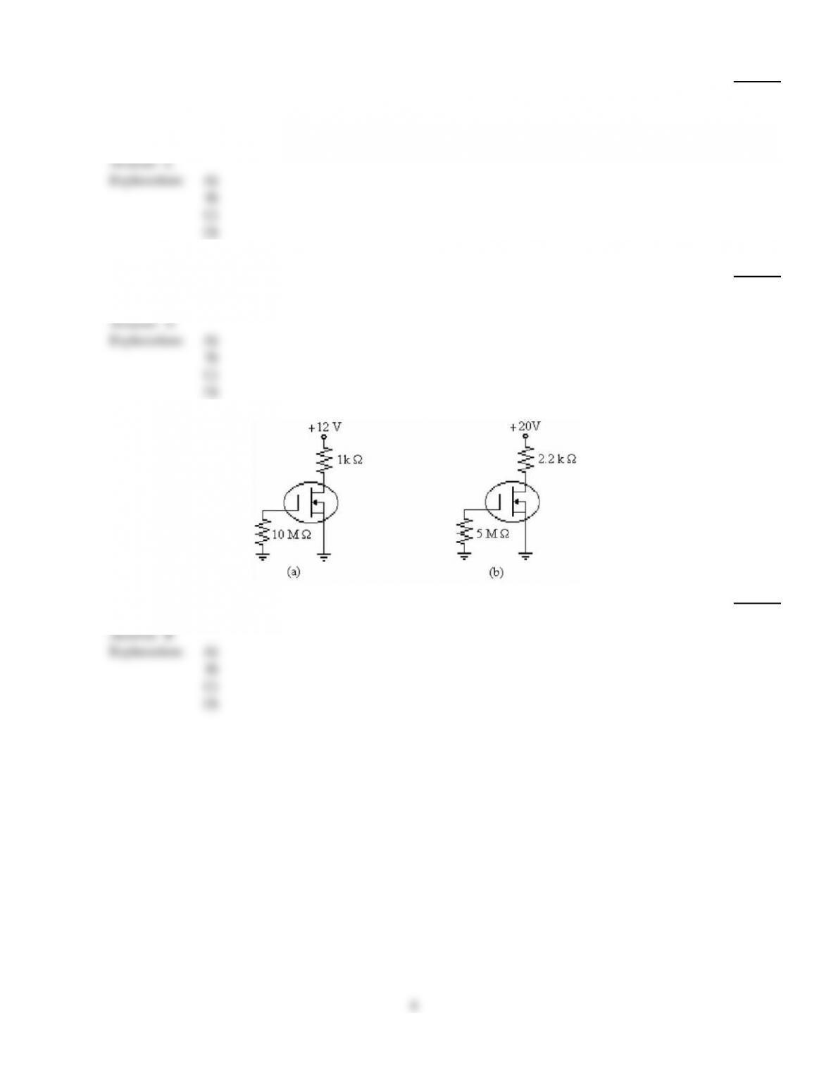
32)
Refer to the figure above. The value of the voltage drop across RD is
32)
A)
3 V.
B)
12 V.
C)
6 V.
D)
20 V.
Answer:
B
Explanation:
A)
B)
C)
D)
33)
An n-channel E–MOSFET conducts when it has
33)
A)
VDS > 0.
B)
VGS > VP.
C)
a thin layer of positive charges in the substrate region near the SiO2 layer.
D)
a thin layer of negative charges in the substrate region near the SiO2 layer.
Answer:
D
Explanation:
A)
B)
C)
D)
34)
The pinch–off voltage has the same magnitude as the
34)
A)
gate–source voltage.
B)
gate voltage.
C)
gate–source cutoff voltage.
D)
drain–source voltage.
Answer:
C
Explanation:
A)
B)
C)
D)
35)
A good application for a V–MOSFET would be as a
35)
A)
substitute for a diode.
B)
low input impedance device.
C)
power amplifier.
D)
low power amplifier.
Answer:
C
Explanation:
A)
B)
C)
D)
9
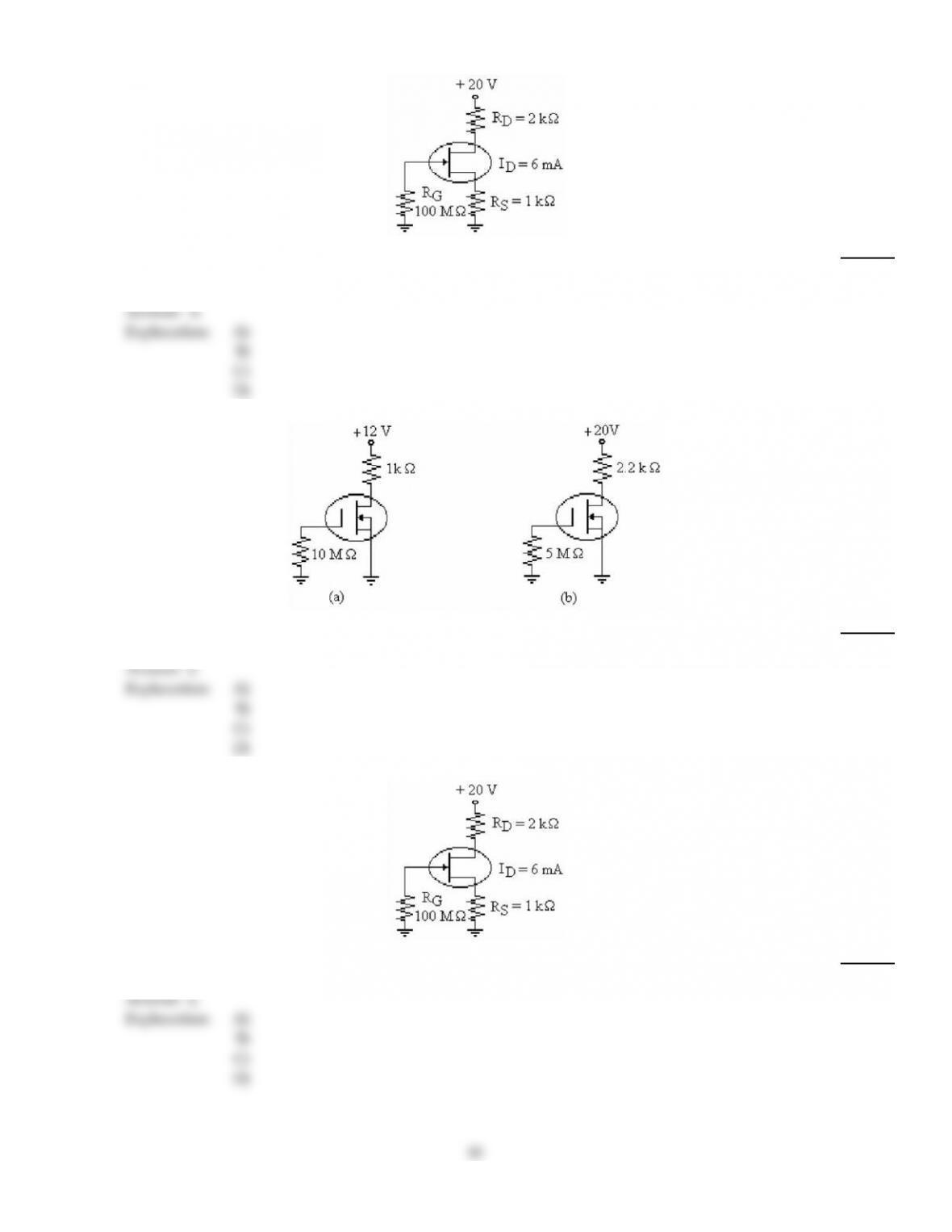
36)
Refer to the figure above. This amplifier is biased for
36)
A)
linear operation.
B)
saturation.
C)
operation as a switch.
D)
pinch–off operation.
Answer:
A
Explanation:
A)
B)
C)
D)
37)
Refer to (b) in the figure above. If ID= 4 mA, the value of VGS is
37)
A)
20 V.
B)
8.8 V.
C)
0 V.
D)
11.2 V.
Answer:
C
Explanation:
A)
B)
C)
D)
38)
Refer to the figure above. Calculate the value of VD.
38)
A)
20 V
B)
6 V
C)
8 V
D)
2 V
Answer:
C
Explanation:
A)
B)
C)
D)
10

39)
A FET that has no IDSS parameter is the
39)
A)
V–MOSFET.
B)
JFET.
C)
E–MOSFET.
D)
DE–MOSFET.
Answer:
C
Explanation:
A)
B)
C)
D)
40)
The type(s) of bias most often used with E–MOSFET circuits is
40)
A)
voltage–divider.
B)
constant current.
C)
drain–feedback.
D)
Both A and C above.
Answer:
D
Explanation:
A)
B)
C)
D)
41)
For a JFET, there is maximum drain current when
41)
A)
the drain and source are interchanged.
B)
VGS equals VGS(off).
C)
VDS is zero.
D)
VGS is zero.
Answer:
D
Explanation:
A)
B)
C)
D)
TRUE/FALSE. Write ‘T’ if the statement is true and ‘F’ if the statement is false.
42)
The JFET operates with a forward–biased gate–source pn junction.
42)
Answer:
True
False
Explanation:
43)
IGBTs are low–power, high–speed devices.
43)
Answer:
True
False
Explanation:
44)
The slope of the characteristic curve in the ohmic region of a JFET is defined by the equation: RDS =
VDS
ID.
44)
Answer:
True
False
Explanation:
45)
JFET data sheets specify input resistance by giving the values for VGS and IDSS.
45)
Answer:
True
False
Explanation:
46)
An E–MOSFET can be used as a switch.
46)
Answer:
True
False
Explanation:
11

47)
The ohmic region of a JFET characteristic curve is roughly parabolic in shape.
47)
Answer:
True
False
Explanation:
48)
Special care is required in handling a MOSFET.
48)
Answer:
True
False
Explanation:
49)
A FET has three terminals named the source, drain, and gate.
49)
Answer:
True
False
Explanation:
50)
Under no signal conditions, midpoint bias allows the maximum amount of drain current swing
between IDSS and zero.
50)
Answer:
True
False
Explanation:
51)
A D–MOSFET can operate with both positive and negative values of VGS.
51)
Answer:
True
False
Explanation:
12