Exam
Name___________________________________
MULTIPLE CHOICE. Choose the one alternative that best completes the statement or answers the question.
1)
The easiest way to bias a JFET in the ohmic region is with
1)
A)
gate bias.
B)
self–bias.
C)
voltage–divider bias.
D)
source bias.
Answer:
C
Explanation:
A)
B)
C)
D)
2)
The simplest method to bias a D–MOSFET is to
2)
A)
set VGS = +4.
B)
set VGS = – 4.
C)
select the correct value RD.
D)
set VGS = 0.
Answer:
D
Explanation:
A)
B)
C)
D)
3)
One advantage of voltage–divider bias is that the dependency of drain current ID, on the range of
Q–points is
3)
A)
reduced.
B)
increased.
C)
not affected.
Answer:
A
Explanation:
A)
B)
C)
4)
For proper operation, an n-channel E–MOSFET should be biased so that VGS is
4)
A)
negative.
B)
positive.
C)
–4 V.
D)
either positive or negative.
Answer:
B
Explanation:
A)
B)
C)
D)
1
5)
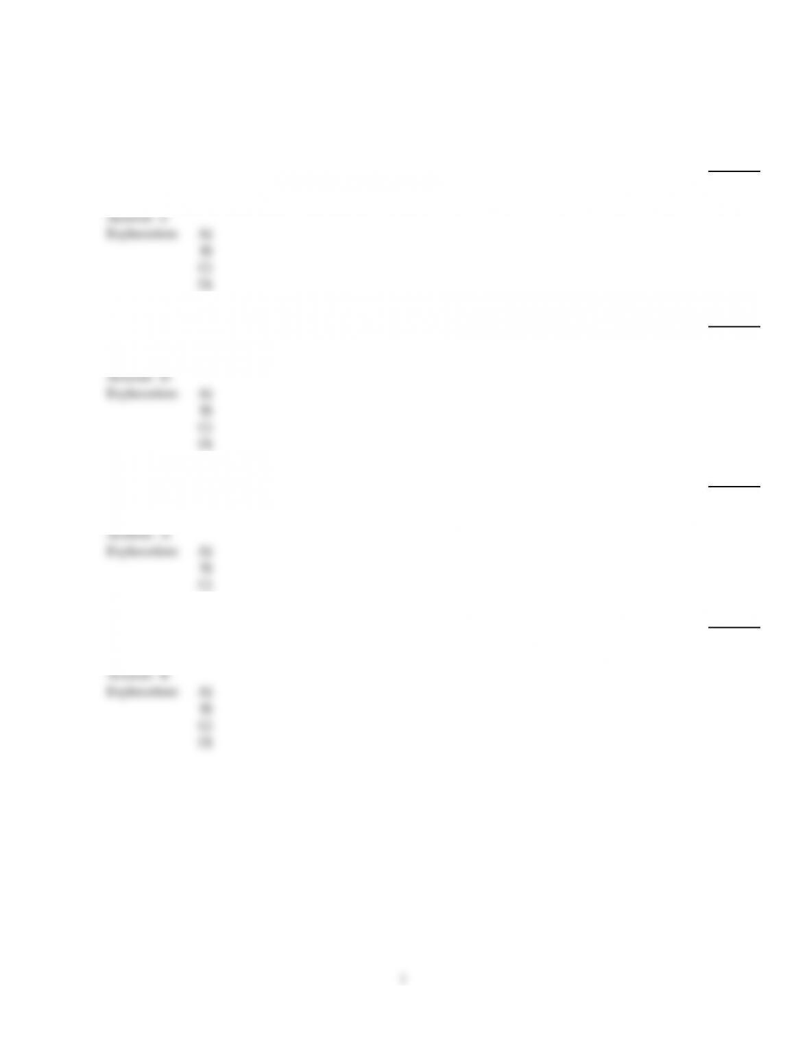
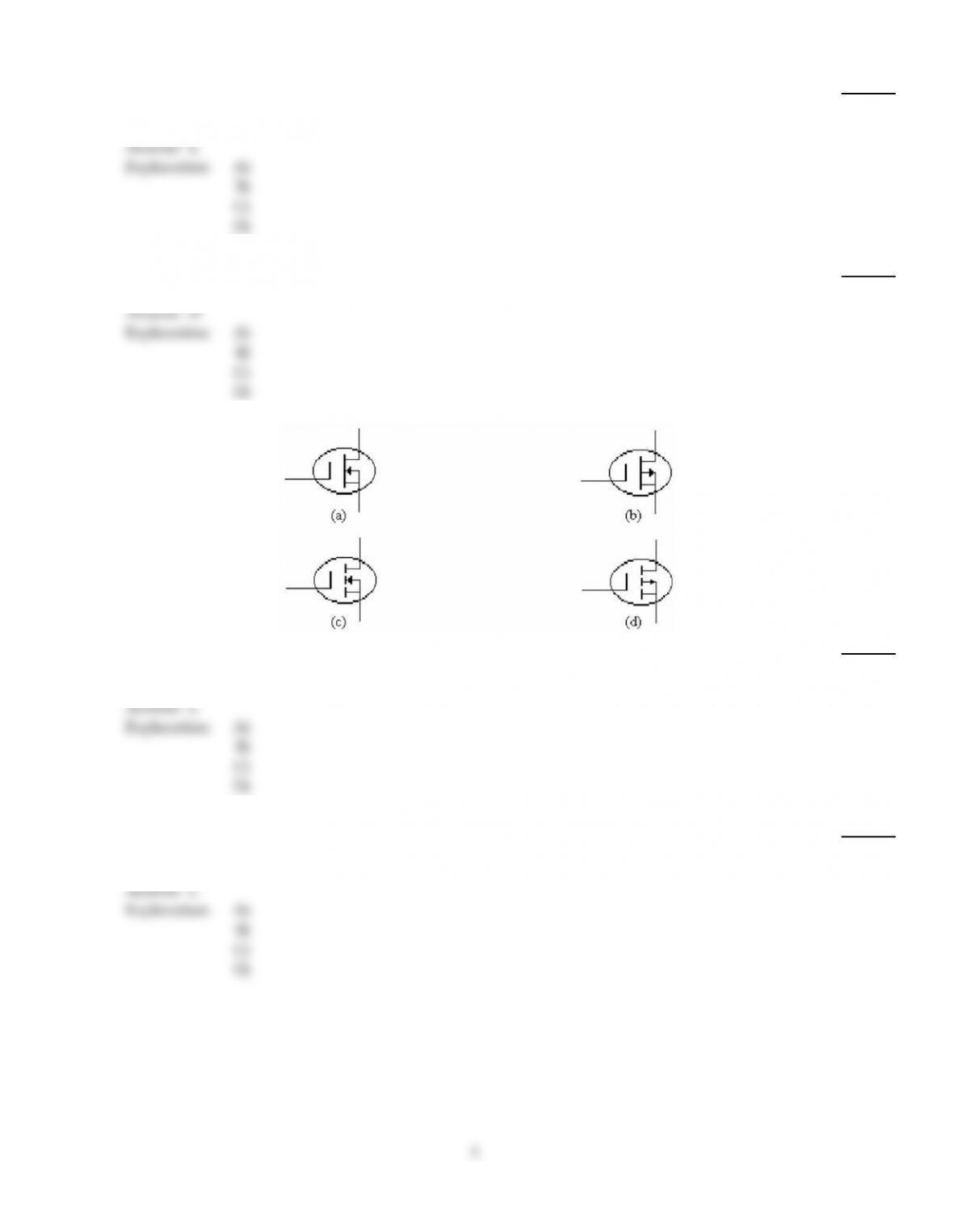
Refer to (c) in the figure above. This symbol identifies
5)
A)
a p-channel E–MOSFET.
B)
a p-channel D–MOSFET.
C)
an n-channel D–MOSFET.
D)
an n-channel E–MOSFET.
Answer:
D
Explanation:
A)
B)
C)
D)
6)
Refer to (a) in the figure above. This symbol identifies
6)
A)
an n-channel D–MOSFET.
B)
a p-channel D–MOSFET.
C)
a p-channel E–MOSFET.
D)
an n-channel E–MOSFET.
Answer:
A
Explanation:
A)
B)
C)
D)
7)
Refer to (b) in the figure above. If ID= 2 mA, the value of VDS is
7)
A)
15.6 V.
B)
20 V.
C)
10 V.
D)
4.4 V.
Answer:
A
Explanation:
A)
B)
C)
D)
2
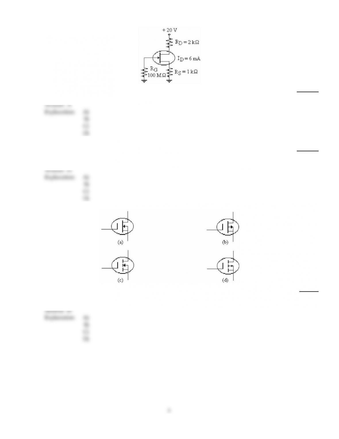
8)
Refer to the figure above. Calculate the value of VDS.
8)
A)
2 V
B)
4 V
C)
0 V
D)
–2 V
Answer:
A
Explanation:
A)
B)
C)
D)
9)
A V–MOSFET device operates in
9)
A)
a JFET mode.
B)
in either enhancement or depletion mode.
C)
the depletion mode.
D)
the enhancement mode.
Answer:
D
Explanation:
A)
B)
C)
D)
10)
Refer to (d) in the figure above. This symbol identifies
10)
A)
an n-channel D–MOSFET.
B)
an n-channel E–MOSFET.
C)
a p-channel D–MOSFET.
D)
a p-channel E–MOSFET.
Answer:
D
Explanation:
A)
B)
C)
D)
3
11)
The gate–source junction of a JFET is
11)
A)
a low resistance path for dc current when reverse–biased.
B)
normally not biased.
C)
normally forward–biased.
D)
normally reverse–biased.
Answer:
D
Explanation:
A)
B)
C)
D)
12)
VDS equals pinch–off voltage divided by the
12)
A)
ideal drain current.
B)
gate current.
C)
drain current for zero gate voltage.
D)
base current.
Answer:
C
Explanation:
A)
B)
C)
D)
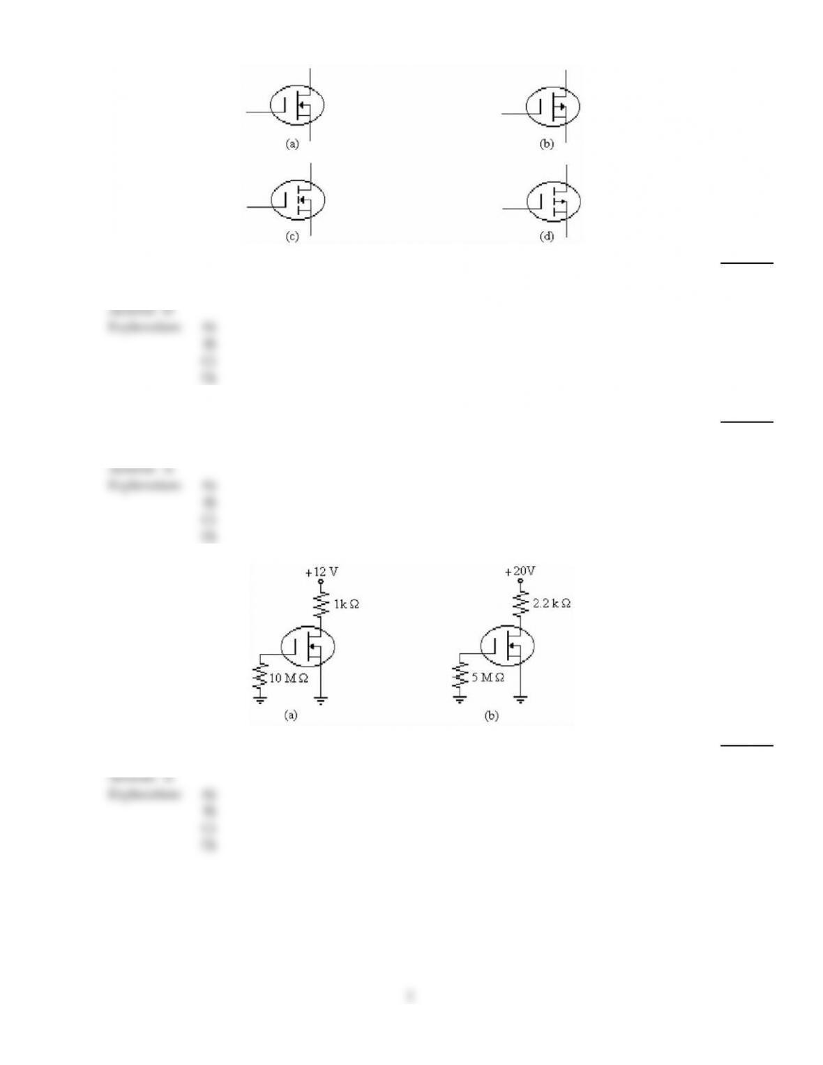
13)
Refer to the figure above. In this circuit, VGS is biased correctly for proper operation. This means
that
VGS is
13)
A)
positive.
B)
either negative or positive.
C)
0 V.
D)
negative.
Answer:
D
Explanation:
A)
B)
C)
D)
14)
When operated in the ohmic area, a JFET acts like a(n)
14)
A)
voltage source.
B)
insulator.
C)
small resistor.
D)
current source.
Answer:
C
Explanation:
A)
B)
C)
D)
4
15)
The FET that has no physical channel is
15)
A)
the JFET.
B)
the D–MOSFET.
C)
the E–MOSFET.
D)
None of the above.
Answer:
C
Explanation:
A)
B)
C)
D)
16)
A ________ change in VDS will produce a ________ change in ID.
16)
A)
large, large
B)
small, large
C)
small, small
D)
large, small
Answer:
D
Explanation:
A)
B)
C)
D)
17)
Refer to (b) in the figure above. This symbol identifies
17)
A)
an n-channel D–MOSFET.
B)
a p-channel E–MOSFET.
C)
a p-channel D–MOSFET.
D)
an n-channel E–MOSFET.
Answer:
C
Explanation:
A)
B)
C)
D)
18)
To get a negative gate–source voltage in a self–biased JFET circuit, you must use a
18)
A)
voltage divider.
B)
ground.
C)
source resistor.
D)
negative gate supply voltage.
Answer:
C
Explanation:
A)
B)
C)
D)
5
19)
The transconductance curve of a JFET is
19)
A)
symmetrical.
B)
nonlinear.
C)
linear.
D)
hyperbolic.
Answer:
B
Explanation:
A)
B)
C)
D)
20)
Field effect transistors are also known as
20)
A)
bipolar devices.
B)
three–charge carrier devices.
C)
unipolar devices.
D)
None of the above.
Answer:
C
Explanation:
A)
B)
C)
D)
21)
IDSS can be defined as the
21)
A)
maximum drain current with the source shorted.
B)
minimum possible drain current.
C)
maximum current drain–to–source with a shorted gate.
D)
maximum possible current with the drain shorted to the source.
Answer:
C
Explanation:
A)
B)
C)
D)
22)
For an enhancement–mode MOSFET, the minimum VGS required to produce drain current is
called the
22)
A)
threshold voltage, designated VGS(th).
B)
IDss.
C)
blocking voltage, designated VB.
D)
breakover voltage.
Answer:
A
Explanation:
A)
B)
C)
D)
23)
The transconductance curve of a JFET is a graph of
23)
A)
IC versus VCE.
B)
ID versus VGS.
C)
IS versus VDS.
D)
ID× RDS.
Answer:
B
Explanation:
A)
B)
C)
D)
6