
26)
Which of the following is not a characteristic of the emitter–follower?
26)
A)
Low output impedance
B)
Voltage gain of 1
C)
Low input impedance
D)
High current gain
Answer:
C
Explanation:
A)
B)
C)
D)
27)
Removing a bypass capacitor from a fully bypassed, common–emitter amplifier circuit will
________ voltage gain and ________ ac input resistance.
27)
A)
increase, increase
B)
increase, decrease
C)
decrease, increase
D)
decrease, decrease
Answer:
C
Explanation:
A)
B)
C)
D)
28)
Often a common–collector will be the last stage before the load; the main function(s) of this stage is
to
28)
A)
buffer the voltage amplifiers from the low resistance load and provide impedance matching
for maximum power transfer.
B)
provide phase inversion.
C)
provide a large voltage gain.
D)
provide a high frequency path to improve the frequency response.
Answer:
A
Explanation:
A)
B)
C)
D)
29)
The input resistance, Rin(base), of a common–emitter amplifier, consists of
29)
A)
RGrcr‘ e.
B)
ac r‘ e.
C)
rer‘ e.
D)
rbre.
Answer:
B
Explanation:
A)
B)
C)
D)
30)
In a swamped amplifier, the effects of r‘ e become
30)
A)
critical to input impedance.
B)
insignificant.
C)
significant to the analysis.
D)
important to voltage gain.
Answer:
B
Explanation:
A)
B)
C)
D)
8

31)
An emitter follower has a voltage gain that is
31)
A)
zero.
B)
greater than one.
C)
much less than one.
D)
approximately equal to one.
Answer:
D
Explanation:
A)
B)
C)
D)
32)
The best selection for a high input impedance amplifier is a
32)
A)
common–base.
B)
high gain common–emitter.
C)
low gain common–emitter.
D)
common–collector.
Answer:
D
Explanation:
A)
B)
C)
D)
33)
Leaving some of the emitter resistance unbypassed in a common–emitter amplifier will
33)
A)
stabilize the voltage gain.
B)
reduce distortion.
C)
increase the input impedance.
D)
All of the above.
Answer:
D
Explanation:
A)
B)
C)
D)
34)
For transistors
34)
A)
the dc current gain is zero.
B)
the dc and ac current gains are the same.
C)
amplification of signal voltage is not possible.
D)
the dc and ac current gains are usually different.
Answer:
D
Explanation:
A)
B)
C)
D)
9
35)
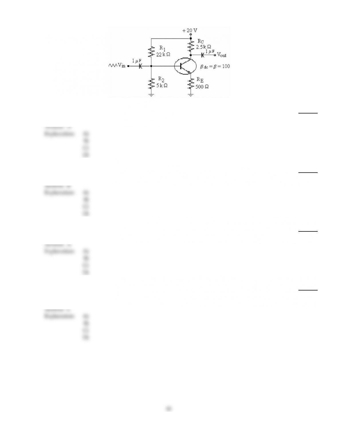
Refer to the figure above. If VE= 0, the trouble might be that
35)
A)
R1 is open.
B)
RC is open.
C)
RE is open.
D)
R2 is open.
Answer:
A
Explanation:
A)
B)
C)
D)
36)
Refer to the figure above. If an emitter–bypass capacitor were installed, AV would be
36)
A)
4.96.
B)
560.
C)
398.
D)
125.
Answer:
B
Explanation:
A)
B)
C)
D)
37)
Refer to the figure above. If R2 opened, VCE would be
37)
A)
0 V.
B)
4.8 V.
C)
20 V.
D)
10 V.
Answer:
A
Explanation:
A)
B)
C)
D)
38)
If two transistors are connected as a Darlington pair and each transistor has a Beta of 175, the
overall current gain of the pair equals
38)
A)
5,000.
B)
3,625.
C)
30,625.
D)
10,000.
Answer:
C
Explanation:
A)
B)
C)
D)
10
39)
Which of the following is not a characteristic of the common–base amplifier?
39)
A)
High input impedance
B)
High output impedance
C)
Current gain of 1
D)
High voltage gain
Answer:
A
Explanation:
A)
B)
C)
D)
40)
A bypass capacitor is placed across the emitter resistor in a voltage–divider biased
common–emitter amplifier circuit. This will
40)
A)
shift the Q–point on the dc load line.
B)
reduce the emitter’s dc voltage to zero.
C)
place the emitter at ac ground.
D)
All of the above.
Answer:
C
Explanation:
A)
B)
C)
D)
41)
Refer to the figure above. The value of VC is
41)
A)
20 V.
B)
6.1 V.
C)
10 V.
D)
0 V.
Answer:
B
Explanation:
A)
B)
C)
D)
42)
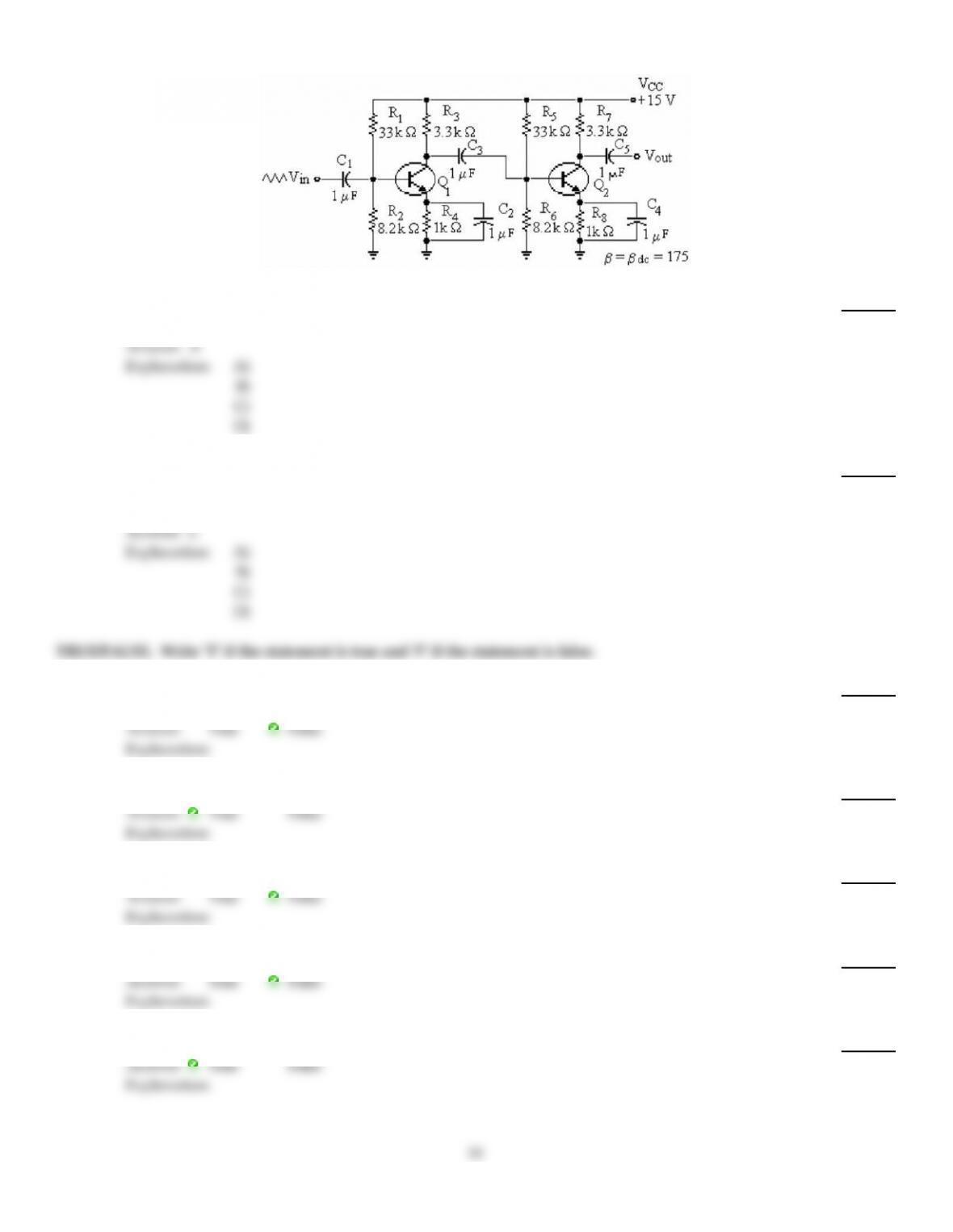
A three–stage amplifier has a gain of 20 for each stage. The overall decibel voltage gain is
42)
A)
400 dB.
B)
78 dB.
C)
8,000 dB.
D)
60 dB.
Answer:
B
Explanation:
A)
B)
C)
D)
11

43)
Where is the output coupling capacitor connected on a common–collector amplifier?
43)
A)
Base
B)
Collector
C)
dc power supply
D)
Emitter
Answer:
D
Explanation:
A)
B)
C)
D)
44)
A differential amplifier provides an output that is the ________ of the two input quantities.
44)
A)
sine
B)
difference
C)
square
D)
multiplication
Answer:
B
Explanation:
A)
B)
C)
D)
45)
A differential amplifier should exhibit a ________ differential gain and a ________ common mode
gain.
45)
A)
low, high
B)
low, low
C)
high, low
D)
high, high
Answer:
C
Explanation:
A)
B)
C)
D)
46)
Reducing all dc sources to zero is done to help obtain the
46)
A)
dc equivalent circuit.
B)
voltage–divider biased circuit.
C)
complete amplifier circuit.
D)
ac equivalent circuit.
Answer:
D
Explanation:
A)
B)
C)
D)
47)
The value of output resistance in a common–emitter amplifier, Rout, consists of
47)
A)
RL+ RC.
B)
RC.
C)
RC.
D)
RL RC.
Answer:
B
Explanation:
A)
B)
C)
D)
12

48)
Increasing the resistance of the load resistor in an RC coupled common–emitter amplifier will have
what effect on voltage gain?
48)
A)
Increases the voltage gain
B)
Decreases the voltage gain
C)
Does not affect the voltage gain
Answer:
A
Explanation:
A)
B)
C)
49)
Removing the emitter bypass capacitor from a common–emitter amplifier
49)
A)
increases Rin and decreases voltage gain.
B)
does not affect Rin.
C)
increases the distortion.
D)
decreases Rin and increases voltage gain.
Answer:
A
Explanation:
A)
B)
C)
D)
50)
Assume that a certain differential amplifier has a differential gain of 3,000 and a common mode
gain of 0.25. What is the CMRR?
50)
A)
750
B)
12,000
C)
66.89
D)
3,025
Answer:
B
Explanation:
A)
B)
C)
D)
51)
In a two–stage amplifier, the input resistance of the second stage
51)
A)
does not affect the voltage gain of the first stage.
B)
affects the voltage gain of the first stage.
C)
is in parallel with the collector resistor of the first stage.
D)
Both B and C above.
Answer:
D
Explanation:
A)
B)
C)
D)
52)
Assume that a certain differential amplifier has a differential gain of 5,000 and a common mode
gain of 0.3. What is the CMRR in dB?
52)
A)
84.44 dB
B)
1,500 dB
C)
62.12 dB
D)
0.3 dB
Answer:
A
Explanation:
A)
B)
C)
D)
13
53)
Refer to the figure above. If AV1 = 75 and AV2 = 95, AVT would be
53)
A)
7125.
B)
75.
C)
1275.
D)
95.
Answer:
A
Explanation:
A)
B)
C)
D)
54)
The h–parameter, hfe, is the same as ________ of the transistor.
54)
A)
maximum collector current
B)
minimum hold current
C)
ac Beta
D)
dc Beta
Answer:
C
Explanation:
A)
B)
C)
D)
TRUE/FALSE. Write ‘T’ if the statement is true and ‘F’ if the statement is false.
55)
A common–emitter amplifier has very high input impedance, high voltage gain, and high current
gain.
55)
Answer:
True
False
Explanation:
56)
A common–collector amplifier is also known as an emitter follower.
56)
Answer:
True
False
Explanation:
57)
A common–base amplifier has a high current gain.
57)
Answer:
True
False
Explanation:
58)
The Sziklai pair uses two PNP transistors.
58)
Answer:
True
False
Explanation:
59)
A high input impedance amplifier could be implemented with a Darlington pair.
59)
Answer:
True
False
Explanation:
14