Exam
Name___________________________________
MULTIPLE CHOICE. Choose the one alternative that best completes the statement or answers the question.
1)
The input resistance of the base of an emitter follower is usually
1)
A)
high.
B)
shorted to ground.
C)
low.
D)
open.
Answer:
A
Explanation:
A)
B)
C)
D)
2)
The best choice for a very high power amplifier is a(n)
2)
A)
common–emitter.
B)
common–collector.
C)
emitter–follower.
D)
common–base.
Answer:
A
Explanation:
A)
B)
C)
D)
3)
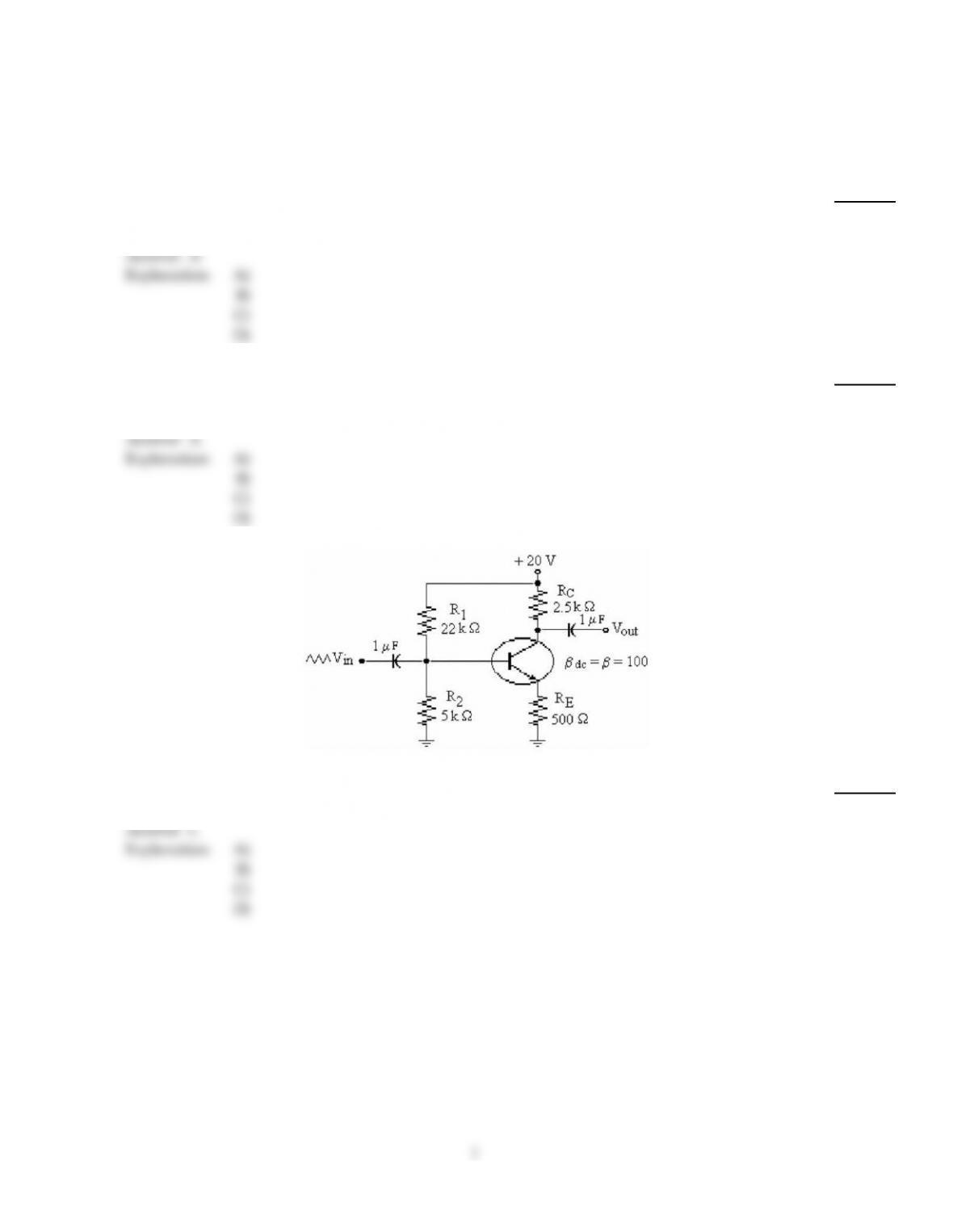
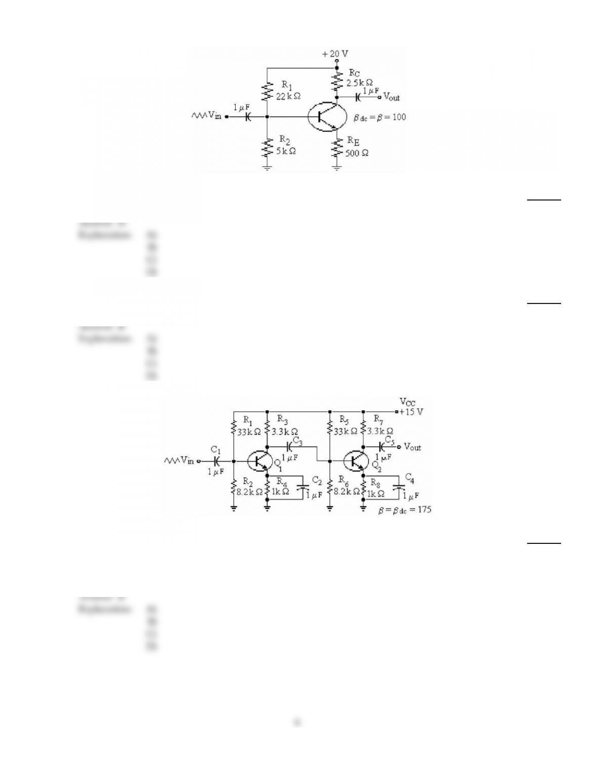
Refer to the figure above. If R2 opened, the value of IC would be
3)
A)
8 mA.
B)
6 mA.
C)
6.67 mA.
D)
10 mA.
Answer:
C
Explanation:
A)
B)
C)
D)
1

4)
The voltage gain of an amplifier is defined as the
4)
A)
ac output voltage divided by the ac input voltage.
B)
ac collector current divided by the ac emitter current.
C)
ac input voltage divided by the ac output voltage.
D)
ac collector current divided by the ac base current.
Answer:
A
Explanation:
A)
B)
C)
D)
5)
The voltage gain of a common–emitter amplifier, AV, can be defined as
5)
A)
AV= IC× RC.
B)
AV=Vb
Vc.
C)
AV=RC
RC+ 1 .
D)
AV=IeRC
Ier’ e.
Answer:
D
Explanation:
A)
B)
C)
D)
6)
To reduce the distortion of an amplified signal, you can increase the
6)
A)
generator resistance.
B)
load resistance.
C)
collector resistance.
D)
emitter feedback resistance.
Answer:
D
Explanation:
A)
B)
C)
D)
7)
The quantity r‘ e
7)
A)
has no effect on gain in transistors.
B)
is external to the transistor.
C)
is a dc value.
D)
is temperature dependent.
Answer:
D
Explanation:
A)
B)
C)
D)
2
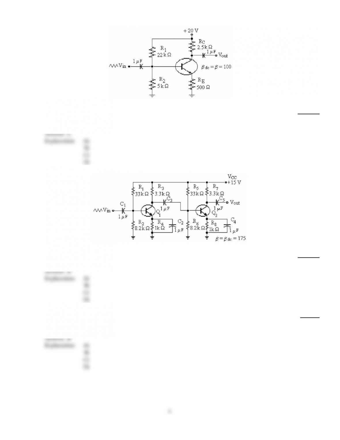
8)
Refer to the figure above. If RC opened, VE would
8)
A)
increase.
B)
remain the same.
C)
decrease.
D)
be undetermined.
Answer:
C
Explanation:
A)
B)
C)
D)
9)
Refer to the figure above. If VB2 were higher than normal, the problem, if any, could be that
9)
A)
C2 is open.
B)
C3 is shorted.
C)
R3 is open.
D)
C1 is open.
Answer:
B
Explanation:
A)
B)
C)
D)
10)
Refer to the figure above. Which of the following faults would account for the output voltage being
lower than normal, but not a complete loss of output voltage?
10)
A)
An open C5
B)
An open C4
C)
An open C3
D)
An open C1
Answer:
B
Explanation:
A)
B)
C)
D)
3
11)
Refer to the figure above. If an emitter–bypass capacitor were added, the voltage gain
11)
A)
would decrease to zero.
B)
would decrease.
C)
would not change.
D)
would increase.
Answer:
D
Explanation:
A)
B)
C)
D)
12)
In a two–stage amplifier, the voltage gain of the first stage is 80 and the voltage gain of the second
stage is 50. How much is the overall voltage gain?
12)
A)
400
B)
130
C)
72
D)
4,000
Answer:
D
Explanation:
A)
B)
C)
D)
13)
If a CE stage is direct coupled to an emitter–follower, how many coupling capacitors are there
between the two stages?
13)
A)
0
B)
1
C)
2
D)
3
Answer:
A
Explanation:
A)
B)
C)
D)
14)
Output resistance in a common–collector amplifier circuit is stepped down by a factor of
14)
A)
Beta .
B)
RE
RL.
C)
r‘e+ re.
D)
alpha .
Answer:
A
Explanation:
A)
B)
C)
D)
4
15)
The capacitor that produces an ac ground at a point in a circuit is called a(n)
15)
A)
ac open.
B)
coupling capacitor.
C)
dc short.
D)
bypass capacitor.
Answer:
D
Explanation:
A)
B)
C)
D)
16)
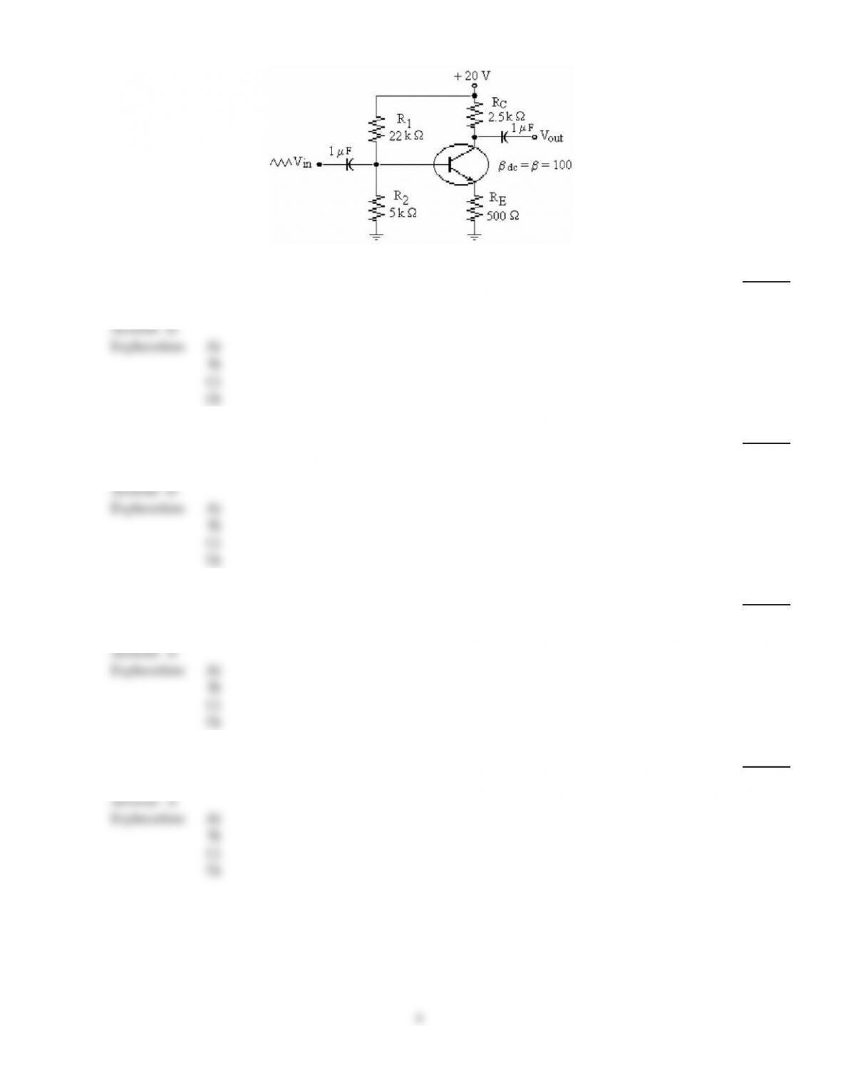
Refer to the figure above. If the collector opened internally, the voltage on the collector would
16)
A)
decrease.
B)
remain the same.
C)
increase.
D)
be undetermined.
Answer:
C
Explanation:
A)
B)
C)
D)
17)
The primary reason an ac load line differs from a dc load line is
17)
A)
changes in current are nonlinear for small–signal amplifier operation.
B)
the effective ac collector resistance is greater than the dc collector resistance.
C)
the effective ac collector resistance is less than the dc collector resistance.
D)
the ac load line is not as steep as the dc load line.
Answer:
C
Explanation:
A)
B)
C)
D)
18)
In general, coupling capacitors can be considered
18)
A)
open for signal voltage and a short for dc.
B)
lossy.
C)
short for signal voltage and an open for dc.
D)
short for signal voltage and a short for dc.
Answer:
C
Explanation:
A)
B)
C)
D)
5
19)
Refer to the figure above. If the emitter collector shorted, the voltage VC would be
19)
A)
20 V.
B)
0 V.
C)
16.67 V.
D)
3.33 V.
Answer:
D
Explanation:
A)
B)
C)
D)
20)
A certain transistor has a dc emitter current of 25 mA. The value of r‘ e is
20)
A)
1.2 .
B)
1 .
C)
2.5 .
D)
25 .
Answer:
B
Explanation:
A)
B)
C)
D)
21)
Refer to the figure above. In servicing this amplifier Vout has a dc component in addition to the
normal ac output voltage. This would be caused by a(n)
21)
A)
open C3.
B)
shorted C5.
C)
open C2.
D)
open base–emitter of C2.
Answer:
B
Explanation:
A)
B)
C)
D)
6

22)
Refer to the figure above. The output signal at the collector of Q1 is higher than normal. This could
be caused by a(n)
22)
A)
open C2.
B)
open C3.
C)
open base–emitter of Q1.
D)
open C1.
Answer:
B
Explanation:
A)
B)
C)
D)
23)
The ac resistance r’ e approximately equals
23)
A)
25 mV
IE.
B)
25 mV
IB.
C)
25 mV
IC.
D)
25 mV × IC.
Answer:
A
Explanation:
A)
B)
C)
D)
24)
For a bypass capacitor to work properly, the
24)
A)
XC should be ten times smaller than RE at the minimum operating frequency.
B)
XC should be twice the value of the RE.
C)
XC should be ten times greater than RE at the minimum operating frequency.
D)
XC should equal RE.
Answer:
A
Explanation:
A)
B)
C)
D)
25)
The three factors that must be taken into account when determining the actual signal voltage at the
base of a small signal bipolar amplifier are
25)
A)
source resistance, collector resistance, internal resistance.
B)
source resistance, bias resistance, and load resistance.
C)
source resistance, emitter resistance, and input resistance.
D)
source resistance, bias resistance, and input resistance.
Answer:
D
Explanation:
A)
B)
C)
D)
7