18)
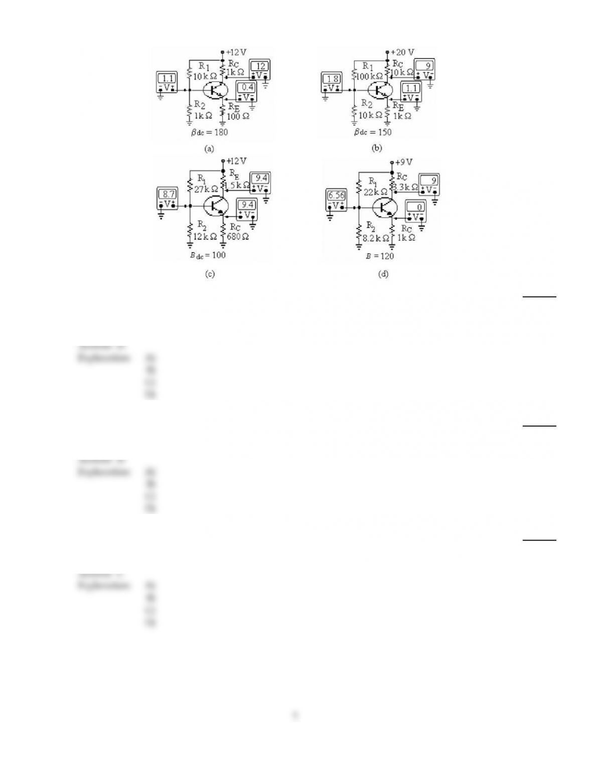
Refer to (b) in the figure above. The most probable cause of trouble, if any, from these voltage
measurements is
18)
A)
the base–emitter junction is open.
B)
a short from collector to emitter.
C)
RE is open.
D)
There are no problems.
Answer:
D
Explanation:
A)
B)
C)
D)
19)
Improper biasing can cause distortion in an amplifier’s
19)
A)
power dissipation.
B)
frequency response.
C)
input signal.
D)
output signal.
Answer:
D
Explanation:
A)
B)
C)
D)
20)
The first step in analyzing emitter–biased circuits is to find the
20)
A)
base current.
B)
transistor power.
C)
emitter voltage.
D)
collector current.
Answer:
C
Explanation:
A)
B)
C)
D)
7
21)
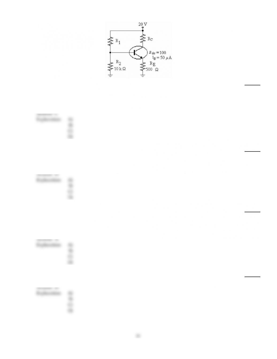
Refer to the figure above. This transistor is biased for ________ operation.
21)
A)
saturation
B)
linear
C)
cutoff
D)
Either A or C above.
Answer:
B
Explanation:
A)
B)
C)
D)
22)
Refer to (a) in the figure above. The most probable cause of trouble, if any, from these voltage
measurements would be
22)
A)
RE is open.
B)
the base–emitter junction is open.
C)
a short from collector to emitter.
D)
There are no problems.
Answer:
A
Explanation:
A)
B)
C)
D)
8
23)
Refer to the figure above. The voltage at the base of this silicon transistor is
23)
A)
12 V.
B)
0 V.
C)
11.3 V.
D)
0.3 V.
E)
0.7 V.
Answer:
E
Explanation:
A)
B)
C)
D)
E)
24)
Refer to the figure above. The purpose of RE is to
24)
A)
maintain VBE at 0.7 V.
B)
develop the output voltage.
C)
establish a dc base voltage.
D)
stabilize the operating point with negative feedback.
Answer:
D
Explanation:
A)
B)
C)
D)
25)
For a properly designed emitter–bias circuit, changes in current gain
25)
A)
affect the collector voltage.
B)
do not occur in the transistor.
C)
severely affect the Q–point.
D)
do not affect the Q–point.
Answer:
D
Explanation:
A)
B)
C)
D)
9
26)
Three different Q–points are shown on a dc load line. The upper Q–point represents the
26)
A)
maximum current gain.
B)
minimum current gain.
C)
intermediate current gain.
D)
cutoff point.
Answer:
A
Explanation:
A)
B)
C)
D)
27)
Adding an emitter resistor to a base–bias circuit produces a bias circuit called
27)
A)
emitter–feedback bias.
B)
base–emitter bias.
C)
emitter bias.
D)
None of the above.
Answer:
A
Explanation:
A)
B)
C)
D)
28)
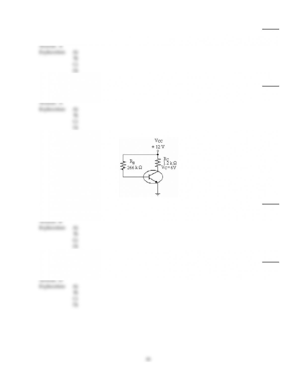
Refer to the figure above. If DC = 100, the minimum value of IB that would cause this transistor to
saturate is
28)
A)
1 mA.
B)
0.1 mA.
C)
50 µA.
D)
100 µA.
Answer:
B
Explanation:
A)
B)
C)
D)
29)
The Q–point of a two supply emitter–bias circuit is not affected by
29)
A)
emitter resistance.
B)
VCC.
C)
collector resistance.
D)
current gain.
Answer:
D
Explanation:
A)
B)
C)
D)
10
30)
Refer to the figure above. The purpose of RC is to
30)
A)
maintain VBE at 0.7 V.
B)
stabilize the operating point with negative feedback.
C)
develop the output voltage.
D)
establish a dc base voltage.
Answer:
C
Explanation:
A)
B)
C)
D)
31)
If the base–emitter junction opens in a voltage–divider biased circuit, the emitter voltage will
measure
31)
A)
0.7 V more than the base.
B)
0.7 V less than the base.
C)
a voltage nearly equal to VCC.
D)
0 V.
Answer:
D
Explanation:
A)
B)
C)
D)
32)
A linear amplifier should have the Q–point located
32)
A)
approximately half–way between saturation and cutoff.
B)
close to saturation.
C)
close to cutoff.
D)
in the distortion region.
Answer:
A
Explanation:
A)
B)
C)
D)
33)
An indication of cutoff is that
33)
A)
VBE = 0.7 V.
B)
IC= IC(sat).
C)
VCE = 0 V.
D)
VCE = VCC.
Answer:
D
Explanation:
A)
B)
C)
D)
11
34)
On a dc load line, the area between saturation and cutoff is called the
34)
A)
depletion region.
B)
linear region.
C)
breakdown region.
D)
saturation zone.
Answer:
B
Explanation:
A)
B)
C)
D)
35)
A certain transistor in a fixed–bias circuit has the following values: IB= 50 µA, DC = 125, VCC =
18 V, and RC= 1.2 k. VC is
35)
A)
7.5 V.
B)
10.5 V.
C)
0 V.
D)
18 V.
Answer:
B
Explanation:
A)
B)
C)
D)
36)
The emitter resistor in a voltage–divider bias circuit is open. The collector voltage will equal
approximately
36)
A)
0 V.
B)
VCC.
C)
one–half VCC.
D)
None of the above.
Answer:
B
Explanation:
A)
B)
C)
D)
TRUE/FALSE. Write ‘T’ if the statement is true and ‘F’ if the statement is false.
37)
A transistor operating in saturation has very little collector current.
37)
Answer:
True
False
Explanation:
38)
Biasing a BJT amplifier means establishing dc operating voltages for proper operation.
38)
Answer:
True
False
Explanation:
39)
Voltage–divider biasing is rarely used due to instability.
39)
Answer:
True
False
Explanation:
40)
Negative feedback in the collector–feedback circuit provides more stable operation.
40)
Answer:
True
False
Explanation:
41)
The correct formula for finding the dc current gain is DC = IC/IB.
41)
Answer:
True
False
Explanation:
12