Exam
Name___________________________________
MULTIPLE CHOICE. Choose the one alternative that best completes the statement or answers the question.
1)
If the collector resistor decreases to zero in a base–biased circuit, the load line will become
1)
A)
useless.
B)
flat.
C)
horizontal.
D)
vertical.
Answer:
D
Explanation:
A)
B)
C)
D)
2)
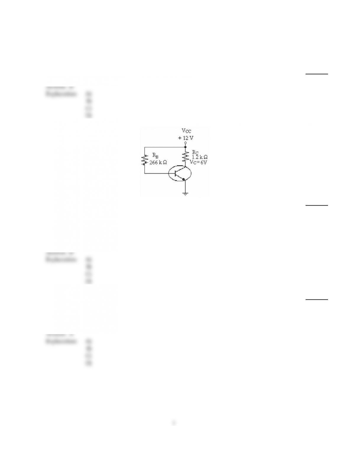
Refer to the figure above. If VC increases to 9 V, which of the following would make the dc
collector voltage return to 6 V?
2)
A)
Replace the transistor with one with a lower dc
B)
Increase the value of RB
C)
Increase VCC
D)
Decrease the value of RB
Answer:
D
Explanation:
A)
B)
C)
D)
3)
For transistors using voltage–divider bias, the base current should be
3)
A)
much smaller than the current through the voltage divider.
B)
Beta times larger than the collector current.
C)
about one–half the collector current.
D)
much larger than the current through the voltage divider.
Answer:
A
Explanation:
A)
B)
C)
D)
1
4)
Refer to the figure above. If the transistor were replaced with a transistor whose dc = 200, the
change that might occur is
4)
A)
VC would change a small amount.
B)
VC would decrease to near 0 V.
C)
IB would increase significantly.
D)
VC would increase to near 20 V.
Answer:
A
Explanation:
A)
B)
C)
D)
5)
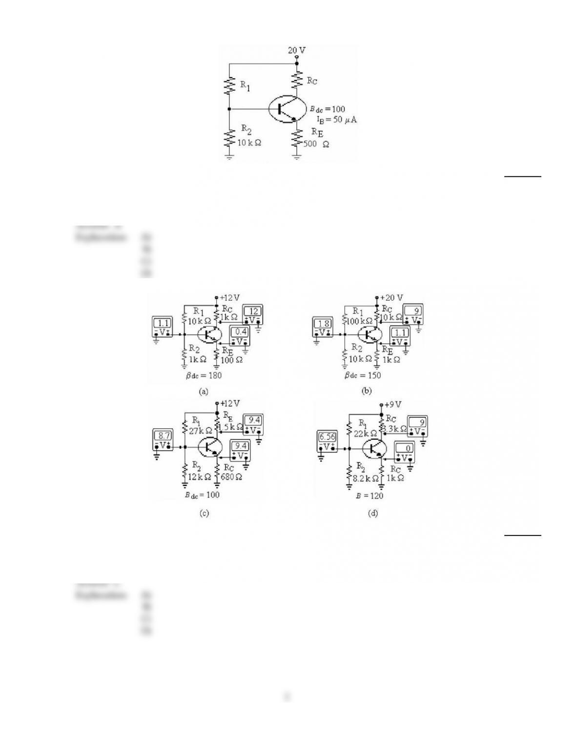
Refer to (d) in the figure above. The most probable cause of trouble, if any, from these voltage
measurements is
5)
A)
a short from collector to emitter.
B)
RE is open.
C)
the base–emitter junction is open.
D)
There are no problems.
Answer:
C
Explanation:
A)
B)
C)
D)
2
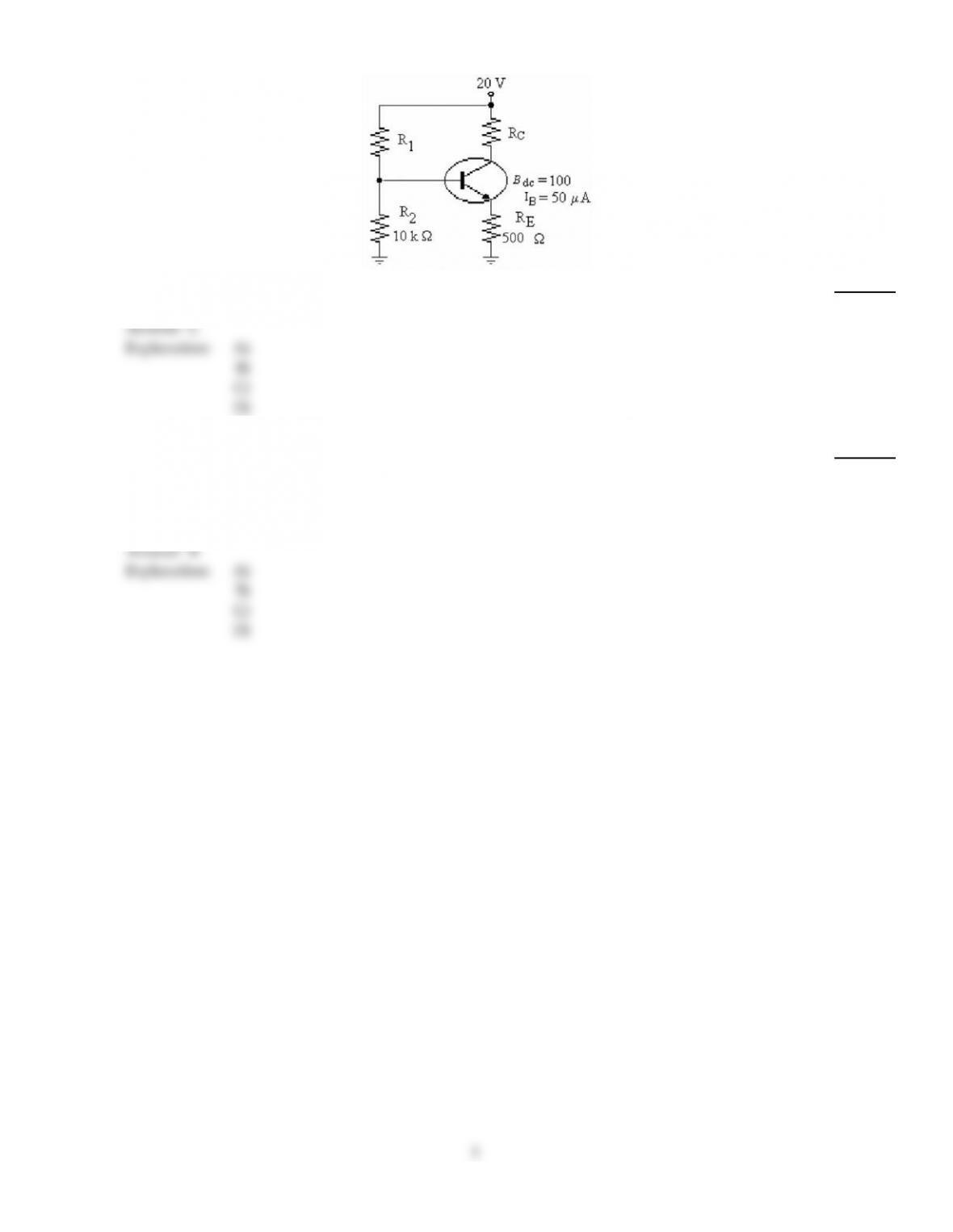
6)
Refer to the figure above. The value of RC that will produce a value of VC= 10 V is
6)
A)
2.2 k.
B)
1 k.
C)
2 k.
D)
500 .
Answer:
C
Explanation:
A)
B)
C)
D)
7)
The main difference between an NPN and PNP transistor amplifier is that
7)
A)
PNP transistors need more heat sinking.
B)
PNP transistors require opposite bias polarities as compared to NPN.
C)
NPN transistors are linear amplifiers, while PNP amplifiers are nonlinear.
D)
PNP transistors cannot amplify sine waves.
Answer:
B
Explanation:
A)
B)
C)
D)
3
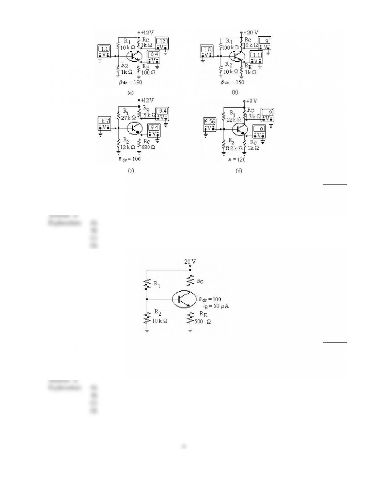
8)
Refer to (c) in the figure above. The most probable cause of trouble, if any, from these voltage
measurements is
8)
A)
a short from collector to emitter.
B)
the base–emitter junction is open.
C)
RE is open.
D)
There are no problems.
Answer:
A
Explanation:
A)
B)
C)
D)
9)
Refer to the figure above. The purpose for R1 and R2 is to
9)
A)
establish a dc base voltage.
B)
maintain VBE at 0.7 V.
C)
stabilize the operating point with negative feedback.
D)
develop the output voltage.
Answer:
A
Explanation:
A)
B)
C)
D)
4

10)
Saturation and cutoff are operating conditions that are very useful when operating the transistor as
10)
A)
a current amplifier.
B)
a switch.
C)
a linear amplifier.
D)
None of the above.
Answer:
B
Explanation:
A)
B)
C)
D)
11)
If a transistor operates at the middle of the dc load line, a decrease in the current gain will move the
Q–point
11)
A)
nowhere.
B)
off the load line.
C)
up.
D)
down.
Answer:
D
Explanation:
A)
B)
C)
D)
12)
Voltage–divider bias provides
12)
A)
a stable Q–point.
B)
an unstable Q–point.
C)
a Q–point that easily varies with changes in the transistor‘s current gain.
D)
Both A and C above.
Answer:
A
Explanation:
A)
B)
C)
D)
13)
The most suitable biasing technique used is the
13)
A)
collector–bias.
B)
emitter–bias.
C)
voltage–divider bias.
D)
base–bias.
Answer:
C
Explanation:
A)
B)
C)
D)
14)
Base bias provides
14)
A)
zero current in the base and collector circuits.
B)
a very unstable Q–point.
C)
no current gain.
D)
a very stable Q–point.
Answer:
B
Explanation:
A)
B)
C)
D)
5
15)
Two important yet easily measured quantities that can help determine if a transistor amplifier is
operating correctly are
15)
A)
dc and IB.
B)
VC and VBE.
C)
IC and VC.
D)
VBE and IE.
Answer:
B
Explanation:
A)
B)
C)
D)
16)
For linear operation, it is usual to set the Q–point so that
16)
A)
VCE = VCC/4.
B)
VCE = VE.
C)
VCE = VCC/2.
D)
VCE = VCC.
Answer:
C
Explanation:
A)
B)
C)
D)
17)
A circuit with a fixed emitter current is called
17)
A)
one–supply bias.
B)
emitter–bias.
C)
base–bias.
D)
grid–bias.
Answer:
B
Explanation:
A)
B)
C)
D)
6